EP0273246A2 - Cellule à cristal liquide et sa méthode de fabrication - Google Patents
Cellule à cristal liquide et sa méthode de fabrication Download PDFInfo
- Publication number
- EP0273246A2 EP0273246A2 EP87118134A EP87118134A EP0273246A2 EP 0273246 A2 EP0273246 A2 EP 0273246A2 EP 87118134 A EP87118134 A EP 87118134A EP 87118134 A EP87118134 A EP 87118134A EP 0273246 A2 EP0273246 A2 EP 0273246A2
- Authority
- EP
- European Patent Office
- Prior art keywords
- substrates
- liquid crystal
- substrate
- transparent electrodes
- rear substrates
- Prior art date
- Legal status (The legal status is an assumption and is not a legal conclusion. Google has not performed a legal analysis and makes no representation as to the accuracy of the status listed.)
- Withdrawn
Links
Images


Classifications
-
- G—PHYSICS
- G02—OPTICS
- G02F—OPTICAL DEVICES OR ARRANGEMENTS FOR THE CONTROL OF LIGHT BY MODIFICATION OF THE OPTICAL PROPERTIES OF THE MEDIA OF THE ELEMENTS INVOLVED THEREIN; NON-LINEAR OPTICS; FREQUENCY-CHANGING OF LIGHT; OPTICAL LOGIC ELEMENTS; OPTICAL ANALOGUE/DIGITAL CONVERTERS
- G02F1/00—Devices or arrangements for the control of the intensity, colour, phase, polarisation or direction of light arriving from an independent light source, e.g. switching, gating or modulating; Non-linear optics
- G02F1/01—Devices or arrangements for the control of the intensity, colour, phase, polarisation or direction of light arriving from an independent light source, e.g. switching, gating or modulating; Non-linear optics for the control of the intensity, phase, polarisation or colour
- G02F1/13—Devices or arrangements for the control of the intensity, colour, phase, polarisation or direction of light arriving from an independent light source, e.g. switching, gating or modulating; Non-linear optics for the control of the intensity, phase, polarisation or colour based on liquid crystals, e.g. single liquid crystal display cells
- G02F1/133—Constructional arrangements; Operation of liquid crystal cells; Circuit arrangements
- G02F1/1333—Constructional arrangements; Manufacturing methods
- G02F1/1339—Gaskets; Spacers; Sealing of cells
Definitions
- the present invention relates to a liquid crystal cell and a manufacturing method thereof.
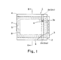
- the conventional liquid crystal cell is constructed as shown in Figs. 1 and 2 of the accompanying drawings, which illustrate a typical liquid crystal cell of dot matrix type.
- the liquid crystal cell of dot matrix type comprises a pair of front and rear glass substrates 2 and 3.
- a plurality of elongated transparent electrodes 2a and 3a formed of indium tin oxide (hereinafter, referred to as "ITO") or the like are first formed respectively on one sides of the respective glass substrates 2 and 3, which face toward each other.
- the electrodes 2a on the front glass substrate 2 are arranged in parallel relation and extend longitudinally in Fig. 1.
- Each of the transparent electrodes 2a is divided at a longitudinally intermediate position into two sections serving as signal-side transparent electrodes 2a1 and 2a2, as clearly shown in Fig. 2.
- the scanning-side transparent electrodes 3a on the rear glass electrode 3 are arranged in parallel relation and extend laterally in Fig. 1.
- Orientation membranes 2b and 3b formed of polyimide or the like are formed respectively on the transparent electrodes 2a and 3a.
- the glass substrates 2 and 3 are then bonded to each other by means of substrate adhesive 4 extending along a periphery of the predetermined gap except for a portion of the periphery thereof, which portion serves as a pouring opening 5.
- Liquid crystal 6 is then filled into the predetermined gap between the glass substrates 2 and 3 through the pouring opening 5 by, for example, a vacuum pouring method. Finally, the pouring opening 5 is closed by a sealing adhesive 7, and a polarizing plate 8 is adhered to the other side of the front glass substrate 2, as clearly shown in Fig. 2, to thereby form the liquid crystal cell 1 of dot matrix type.
- a plurality of spacers 4a each comprising a glass fiber cut in short length are embedded in the substrate adhesive 4, and/or similar spacers 9 having an outer diameter less than that of the spacers 4 are distributed over the gap between the orientation membranes 2b and 3b, as shown in Fig. 2.
- the substrate adhesive 4 is previously applied onto the periphery of the one side of one of the glass substrates 2 and 3 by a screen printing method.
- the substrate adhesive 4 is heated while the glass substrates 2 and 3 are pressed against each other by, for example, a pair of metallic clamping plates, to thereby bond the glass substrates 2 and 3 to each other.
- each of the signal-side transparent electrodes 2a is divided at the longitudinally intermediate position into two sections 2a1 and 2a2.
- the width of the substrate adhesive 4 applied to the peripheries of the respective glass substrates 2 and 3 is relatively wide, resulting in a decrease in an area of an effective display region B of the liquid crystal cell 1.
- the manufacturing cost is increased because of the increase in the areas of the respective glass substrates 2 and 3 which are required for a predetermined effective display area.
- portions of each liquid crystal cell 1, where no display is effected are large in area so that heavy or thick lines, where no display is effected, run longitudinally and laterally on the display screen of the large display device 10. This makes difficult to watch the display, to thereby deteriorate the display quality.
- a liquid crystal cell comprising: a pair of front and rear transparent flat substrates arranged in facing and spaced relation to each other; a plurality of transparent electrodes formed on one side of the front substrate, and a plurality of transparent electrodes formed on one side of the rear substrate which faces toward the one side of the front substrate; orientation membranes formed respectively on the transparent electrodes on the respective front and rear substrates so as to cover the respective transparent electrodes, with a predetermined gap maintained between the one sides of the respective front and rear substrates; substrate adhesive means arranged between the orientation membranes on the respective front and rear substrates at a plurality of areas except for display areas where the transparent electrodes on the respective substrates face toward each other, for bonding the front and rear substrates to each other, with the predetermined gap maintained therebetween; sealing adhesive means extending between the one sides of the respective front and rear substrates and along a periphery of the predetermined gap to define a sealed space between the front and rear substrates; and a liquid crystal filled in the sealed space.
- a method of manufacturing a liquid crystal cell comprising the steps of: preparing a pair of front and rear transparent flat substrates, each of the substrates having a plurality of transparent electrodes formed on one side of the substrate and a transparent orientation membrane formed on the transparent electrodes so as to cover the same; printing a substrate adhesive onto a plurality of areas on the orientation membrane on at least one of the front and rear substrates; superposing the front and rear substrates one upon the other in such a manner that the orientation membranes on the respective substrates face toward each other in spaced relation, but are brought into contact with each other through the printed substrate adhesive, the plurality of areas being those except for display areas where the electrodes on the respective front and rear substrates face toward each other; heating the substrate adhesive to bond the front and rear substrates to each other, with a predetermined gap maintained therebetween; applying a sealing adhesive to the front and rear substrates so as to extend between the one sides of the respective substrates and along a periphery of the predetermined gap to define a
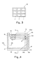
- the liquid crystal cell 11 comprises a pair of front and rear flat glass substrates 12 and 13.
- a plurality of parallel transparent electrodes 12a in the form of an elongated strip and formed of ITO (indium tin oxide) or the like are formed on one side 12d of the glass substrate 12, and similar transparent electrodes 13a are formed on one side 13d of the glass substrate 13 which faces toward the one side 12d of the glass substrate 12.
- Orientation membranes 12b and 13b formed of polyimide or the like are formed respectively on the transparent electrodes 12a and 13a so as to respectively cover the same.
- Both the glass substrates 12 and 13 are superposed one upon the other in such a manner that the orientation membranes 12b and 13b face toward each other in spaced relation, and the transparent electrodes 12a and 13a face toward each other and are perpendicularly intersected with each other.
- Each of the transparent electrodes 12a or each of the transparent electrodes 13a that is to say, each of the transparent electrodes 12a in case of the illustrated embodiment is divided at a longitudinally intermediate position into two sections 12a1 and 12a2, in order to increase the number of dots A displayed by time-division actuation, as many as possible, to enable detailed display.
- a substrate adhesive 14 in the form of a spot is previously printed onto the orientation membrane on at least one of the glass substrates 12 and 13, that is to say, onto the orientation membrane 13b on the rear glass substrate 13 in case of the illustrated embodiment, at a plurality of areas except for display areas where the transparent electrodes 12a and 13a on the respective glass substrates 12 and 13 face toward each other.
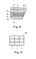
- the substrate adhesive may be in the form of an elongated strip 114 as illustrated in Fig. 6.
- the substrate adhesive 14 is heated while the glass substrates 12 and 13 are pressed against each other, to bond the glass substrates 12 and 13 to each other to secure the same to each other in a united fashion, with a predetermined gap maintained between the glass substrates 12 and 13.
- the substrate adhesive 14 is printed in such a size or dimension that even if the substrate adhesive 14 is spread flat when pressed and heated, it does not enter the display areas formed by the transparent electrodes. Further, in order to maintain the predetermined gap between the glass substrates 2 and 13, spacers 15 each comprising a glass fiber cut in short length are distributed over the surface of the orientation membrane 13b, and/or the spacers 15 are embedded in the substrate adhesive 14. It is appropriately selected depending upon the size of the liquid crystal cell, the size of the display pattern and the like whether only the former way is used, or only the latter way is used, or both the ways are used.
- a sealing adhesive 16 is applied to the glass substrates 12 and 13 so as to extend between their respective one sides 12d and 13d and along the periphery of the predetermined gap between the glass substrates 12 and 13 superposed one upon the other and fixedly secured to each other in the above-described manner.
- a heat curing method, a ultraviolet curing method or the like is employed to bond the glass substrates 12 and 13 by the sealing adhesive 16, to define a sealed space between the glass substrates 12 and 13.
- the sealing adhesive 16 is applied to the glass substrates 12 and 13 except for a portion of the periphery of the predetermined gap to form a pouring opening 17 as illustrated in Fig. 7.
- a liquid crystal 18 is filled in the sealed space between the glass substrates 12 and 13 through the pouring opening 17 by, for example, a vacuum pouring method.
- the same sealing adhesive 16 is applied to the pouring opening 17 and is cured to close the same as illustrated in Fig. 4.
- side edges of the one side 13d of the rear glass substrate 13 except for the right side edge as viewed in Fig. 4 are chamfered at 13c by grinding as illustrated in Figs. 5 and 8, in order to realize the uniform application of the sealing adhesive 16.
- the left side edge of the one side 12d of the front glass substrate 12 as viewed in Fig. 4 may likewise be chamfered at 12c as illustrated in Fig. 8.
- a polarizing plate 19 is adhered to the other side 12e of the glass substrate 12, as illustrated in Fig. 5, so that the liquid crystal cell 11 is completed.
- the liquid crystal cell 11 of dot matrix type is constructed as described above, and the operation of the cell 11 is substantially identical with that of the conventional liquid crystal cell of dot matrix type and will not therefore be described here.
- the substrate adhesive 14 which provides sufficient bonding strength between the glass substrates 12 and 13
- the sealing adhesive 16 for sealing the liquid crystal 18 at the periphery of the predetermined gap between the glass substrates 12 and 13 can be narrowed in width.
- the embodiment of the invention has been described as being applied to the liquid crystal cell of dot matrix type, the invention should not be limited to this specific embodiment, but is applicable to liquid crystal cells having another display patterns.
- the substrates have been described as being formed of glass, they may be formed of any transparent resin materials.
- the substrate adhesive is applied to the front and rear substrates so as to extend between their respective one sides and along the periphery of the predetermined gap between the front and rear substrates.
- This makes it possible to provide the bonding strength between the front and rear substrates, which is similar in degree to that of the conventional liquid crystal cell.
- the sealing adhesive applied to the front and rear substrates along the periphery of the predetermined gap between the substrates can be reduced in width.
Landscapes
- Physics & Mathematics (AREA)
- Nonlinear Science (AREA)
- Liquid Crystal (AREA)
- Mathematical Physics (AREA)
- Chemical & Material Sciences (AREA)
- Crystallography & Structural Chemistry (AREA)
- General Physics & Mathematics (AREA)
- Optics & Photonics (AREA)
- Devices For Indicating Variable Information By Combining Individual Elements (AREA)
Applications Claiming Priority (2)
| Application Number | Priority Date | Filing Date | Title |
|---|---|---|---|
| JP31067686A JPS63165823A (ja) | 1986-12-27 | 1986-12-27 | 液晶セルの構造 |
| JP310676/86 | 1986-12-27 |
Publications (2)
| Publication Number | Publication Date |
|---|---|
| EP0273246A2 true EP0273246A2 (fr) | 1988-07-06 |
| EP0273246A3 EP0273246A3 (fr) | 1989-11-08 |
Family
ID=18008111
Family Applications (1)
| Application Number | Title | Priority Date | Filing Date |
|---|---|---|---|
| EP87118134A Withdrawn EP0273246A3 (fr) | 1986-12-27 | 1987-12-08 | Cellule à cristal liquide et sa méthode de fabrication |
Country Status (2)
| Country | Link |
|---|---|
| EP (1) | EP0273246A3 (fr) |
| JP (1) | JPS63165823A (fr) |
Cited By (2)
| Publication number | Priority date | Publication date | Assignee | Title |
|---|---|---|---|---|
| EP0288304A3 (en) * | 1987-04-22 | 1990-01-24 | Sharp Kabushiki Kaisha | Liquid crystal display device |
| CN102967967A (zh) * | 2012-12-14 | 2013-03-13 | 福耀玻璃工业集团股份有限公司 | 一种用于调光体间隔粒子的粘接层的粘结强度的控制方法 |
Families Citing this family (2)
| Publication number | Priority date | Publication date | Assignee | Title |
|---|---|---|---|---|
| JPH01142617A (ja) * | 1987-11-30 | 1989-06-05 | Fuji Photo Film Co Ltd | 液晶表示素子用セル及びその製造方法 |
| JP2015141208A (ja) * | 2014-01-27 | 2015-08-03 | セイコーエプソン株式会社 | 液晶装置、液晶装置の製造方法および電子機器 |
Family Cites Families (10)
| Publication number | Priority date | Publication date | Assignee | Title |
|---|---|---|---|---|
| JPS5262454A (en) * | 1975-11-18 | 1977-05-23 | Omron Tateisi Electronics Co | Manufacture of display device |
| JPS5717923A (en) * | 1980-07-04 | 1982-01-29 | Matsushita Electric Ind Co Ltd | Manufacture for picture image display panel |
| JPS5886518A (ja) * | 1981-11-18 | 1983-05-24 | Mitsubishi Electric Corp | 液晶表示装置 |
| JPS5897023A (ja) * | 1981-12-04 | 1983-06-09 | Sharp Corp | 液晶表示セル及びその製造方法 |
| JPS59218425A (ja) * | 1983-05-25 | 1984-12-08 | Sharp Corp | 液晶表示素子 |
| JPS6098420A (ja) * | 1983-11-04 | 1985-06-01 | Oki Electric Ind Co Ltd | 液晶パネルの製造方法 |
| JPS60149024A (ja) * | 1984-01-13 | 1985-08-06 | Seiko Epson Corp | 液晶表示装置 |
| JPS60203915A (ja) * | 1984-03-28 | 1985-10-15 | Matsushita Electric Ind Co Ltd | 大型液晶デイスプレイ |
| JPS617824A (ja) * | 1984-06-22 | 1986-01-14 | Canon Inc | 液晶素子 |
| JPS61183625A (ja) * | 1985-02-08 | 1986-08-16 | Matsushita Electric Ind Co Ltd | 液晶表示パネルの製造法 |
-
1986
- 1986-12-27 JP JP31067686A patent/JPS63165823A/ja active Pending
-
1987
- 1987-12-08 EP EP87118134A patent/EP0273246A3/fr not_active Withdrawn
Cited By (3)
| Publication number | Priority date | Publication date | Assignee | Title |
|---|---|---|---|---|
| EP0288304A3 (en) * | 1987-04-22 | 1990-01-24 | Sharp Kabushiki Kaisha | Liquid crystal display device |
| CN102967967A (zh) * | 2012-12-14 | 2013-03-13 | 福耀玻璃工业集团股份有限公司 | 一种用于调光体间隔粒子的粘接层的粘结强度的控制方法 |
| CN102967967B (zh) * | 2012-12-14 | 2014-12-17 | 福耀玻璃工业集团股份有限公司 | 一种用于调光体间隔粒子的粘接层的粘结强度的控制方法 |
Also Published As
| Publication number | Publication date |
|---|---|
| JPS63165823A (ja) | 1988-07-09 |
| EP0273246A3 (fr) | 1989-11-08 |
Similar Documents
| Publication | Publication Date | Title |
|---|---|---|
| JP3698749B2 (ja) | 液晶セルの作製方法およびその作製装置、液晶セルの生産システム | |
| JPS63128315A (ja) | 液晶表示素子 | |
| JPS63110425A (ja) | 液晶封入用セル | |
| JPH0820627B2 (ja) | 液晶表示素子の製造法 | |
| JPS5825617A (ja) | 液晶表示装置およびその製法 | |
| EP0273246A2 (fr) | Cellule à cristal liquide et sa méthode de fabrication | |
| JPS63216027A (ja) | 電気光学装置およびその製造方法 | |
| JP2003005198A (ja) | 液晶表示装置のシーリング構造及びシーリング方法 | |
| JPH03163418A (ja) | 液晶素子 | |
| JP3470871B2 (ja) | 液晶表示パネルの製造方法 | |
| JPS6247286B2 (fr) | ||
| TWI225558B (en) | Liquid crystal display and fabrication method thereof | |
| JPH07318953A (ja) | 液晶表示素子 | |
| JP2004029552A (ja) | 液晶表示素子の製法 | |
| JPH09179132A (ja) | 液晶表示素子における液晶注入孔の封止方法 | |
| JPH0460612A (ja) | 液晶表示器及びその製造方法 | |
| JPS5770521A (en) | Production of liquid crystal display device | |
| JPH0772489A (ja) | 液晶表示素子 | |
| JPH0248824Y2 (fr) | ||
| JPH06294965A (ja) | 液晶表示装置 | |
| KR940009166B1 (ko) | 칼라 액정표시장치의 제조방법 | |
| JPS59176727A (ja) | 液晶表示素子の製造方法 | |
| JP3105386B2 (ja) | 液晶表示パネルおよび液晶表示装置の製法 | |
| JPH01134334A (ja) | 液晶表示装置の製造方法 | |
| JPS62262824A (ja) | 液晶セルの製造方法 |
Legal Events
| Date | Code | Title | Description |
|---|---|---|---|
| PUAI | Public reference made under article 153(3) epc to a published international application that has entered the european phase |
Free format text: ORIGINAL CODE: 0009012 |
|
| AK | Designated contracting states |
Kind code of ref document: A2 Designated state(s): CH DE FR GB IT LI NL SE |
|
| PUAL | Search report despatched |
Free format text: ORIGINAL CODE: 0009013 |
|
| AK | Designated contracting states |
Kind code of ref document: A3 Designated state(s): CH DE FR GB IT LI NL SE |
|
| STAA | Information on the status of an ep patent application or granted ep patent |
Free format text: STATUS: THE APPLICATION IS DEEMED TO BE WITHDRAWN |
|
| 18D | Application deemed to be withdrawn |
Effective date: 19900509 |