EP0273652A2 - Pseudostatische Speichereinrichtung mit einer internen Selbstauffrischungsschaltung - Google Patents
Pseudostatische Speichereinrichtung mit einer internen Selbstauffrischungsschaltung Download PDFInfo
- Publication number
- EP0273652A2 EP0273652A2 EP87311150A EP87311150A EP0273652A2 EP 0273652 A2 EP0273652 A2 EP 0273652A2 EP 87311150 A EP87311150 A EP 87311150A EP 87311150 A EP87311150 A EP 87311150A EP 0273652 A2 EP0273652 A2 EP 0273652A2
- Authority
- EP
- European Patent Office
- Prior art keywords
- access
- circuit
- address
- refresh
- signal
- Prior art date
- Legal status (The legal status is an assumption and is not a legal conclusion. Google has not performed a legal analysis and makes no representation as to the accuracy of the status listed.)
- Granted
Links
Images




Classifications
-
- G—PHYSICS
- G11—INFORMATION STORAGE
- G11C—STATIC STORES
- G11C11/00—Digital stores characterised by the use of particular electric or magnetic storage elements; Storage elements therefor
- G11C11/21—Digital stores characterised by the use of particular electric or magnetic storage elements; Storage elements therefor using electric elements
- G11C11/34—Digital stores characterised by the use of particular electric or magnetic storage elements; Storage elements therefor using electric elements using semiconductor devices
-
- G—PHYSICS
- G11—INFORMATION STORAGE
- G11C—STATIC STORES
- G11C11/00—Digital stores characterised by the use of particular electric or magnetic storage elements; Storage elements therefor
- G11C11/21—Digital stores characterised by the use of particular electric or magnetic storage elements; Storage elements therefor using electric elements
- G11C11/34—Digital stores characterised by the use of particular electric or magnetic storage elements; Storage elements therefor using electric elements using semiconductor devices
- G11C11/40—Digital stores characterised by the use of particular electric or magnetic storage elements; Storage elements therefor using electric elements using semiconductor devices using transistors
- G11C11/401—Digital stores characterised by the use of particular electric or magnetic storage elements; Storage elements therefor using electric elements using semiconductor devices using transistors forming cells needing refreshing or charge regeneration, i.e. dynamic cells
- G11C11/4063—Auxiliary circuits, e.g. for addressing, decoding, driving, writing, sensing or timing
- G11C11/407—Auxiliary circuits, e.g. for addressing, decoding, driving, writing, sensing or timing for memory cells of the field-effect type
- G11C11/408—Address circuits
-
- G—PHYSICS
- G11—INFORMATION STORAGE
- G11C—STATIC STORES
- G11C11/00—Digital stores characterised by the use of particular electric or magnetic storage elements; Storage elements therefor
- G11C11/21—Digital stores characterised by the use of particular electric or magnetic storage elements; Storage elements therefor using electric elements
- G11C11/34—Digital stores characterised by the use of particular electric or magnetic storage elements; Storage elements therefor using electric elements using semiconductor devices
- G11C11/40—Digital stores characterised by the use of particular electric or magnetic storage elements; Storage elements therefor using electric elements using semiconductor devices using transistors
- G11C11/401—Digital stores characterised by the use of particular electric or magnetic storage elements; Storage elements therefor using electric elements using semiconductor devices using transistors forming cells needing refreshing or charge regeneration, i.e. dynamic cells
- G11C11/406—Management or control of the refreshing or charge-regeneration cycles
Definitions
- the present invention relates to a pseudo-static memory device and, more particularly, to a pseudo-static random access memory (PSRAM) device internally having dynamic RAM (DRAM) cells and a circuit for automatically carrying out a refresh for the cells, while functioning as a static RAM (SRAM) in appearance.
- PSRAM pseudo-static random access memory
- a PSRAM has recently been proposed as a memory having both the advantages of a DRAM, i.e. low cost, and an SRAM, i.e. high integration density, and can be widely used in information apparatus such as computers, electronic apparatuses, and the like.
- Such a PSRAM device includes an access circuit for internal refresh, an access circuit for external address access, means for selecting either of the access circuits, and a memory cell array.
- the external address access circuit further includes a circuit for generating a control signal in response to an external signal and a peripheral circuit for carrying out an access to the memory cells in the array in response to the control signal and an address signal.
- the address signal is fed to the PSRAM device by another device for feeding the address signal, e.g. a microprocessor.
- the selecting means are generally arranged to select either the refresh address signal output from the internal refresh access circuit or the external address signal output from the external address access circuit, in accordance with a timing of the input of the address signal.
- the external address access operation is carried out as quickly as possible, from the view point of the demands for a high speed operation of the PSRAM device. Therefore, it is necessary for the aforementioned device for feeding the address signal to feed an address signal consisting of a plurality of address bits to the PSRAM device at a high speed. In this case, the following drawback occurs.
- the timings of the change in address among the plurality of address bits are not completely uniform; namely, generally a time lag or lead occurs (hereinafter referred to as an address skew).
- address skew moves outside a permissible range, a drawback occurs in that another memory cell different from the memory cell to be selected, is selected. Therefore, the timing of the address bits must be strictly controlled in the address signal feeding device, and this means that the constitution of the device becomes complicated and the cost thereof rises.
- Another previously-proposed PSRAM device employs a low active chip enable signal ( CE) as the aforementioned external signal.
- CE active chip enable signal
- another drawback occurs in that the timing of the application of the address signal must be strictly set in association with the timing of the application of the external signal ( CE). That is, there is a disadvantage that only a small allowance is made for the address skew.
- a pseudo-static memory device capable of providing a greater allowance for an address skew and providing a larger allowance for the lag or lead of a timing of the application of an address signal, without complicating the constitution of a device supplying the address signal.
- a pseudo-static memory device receiving at least an external address signal, the device comprising: a memory cell array having a memory cell provided at each intersection between a plurality of word lines and a plurality of bit lines; a first access circuit for carrying out a sequential access to addresses of the word lines to perform a refresh of the memory cell; a second access circuit for bringing one of the word lines to an accessible state in response to the address signal; an access selection circuit operatively connected between the first access circuit and the second access circuit for selecting any one of the access circuits in accordance with the access sequence and performing an address access by the selected access circuit to the memory cell array; a circuit for generating a control signal in response to a change in address of the address signal; and a delay unit operatively connected between the control signal generating circuit and the second access circuit for delaying the control signal by a predetermined time required for performing the refresh of the memory cell, and feeding the delayed control signal to the second access circuit, whereby the second access circuit performs an address access of
- a pseudo-static memory device receiving at least an external address signal, the device comprising: a memory cell array having a memory cell provided at each intersection between a plurality of word lines and a plurality of bit lines; a first access circuit for carrying out a sequential access of addresses of the word lines to perform a refresh of the memory cell; a second access circuit for bringing one of the word lines to an accessible state in response to the address signal; an access selection circuit operatively connected between the first access circuit and the second access circuit for selecting any one of the access circuits in accordance with the access sequence and performing an address access by said selected access circuit to the memory cell array; a circuit for generating a control signal in response to a change in level of an external clock signal; and a delay circuit operatively connected between the control signal generating circuit and the second access circuit for delaying the control signal by a predetermined time required for performing the refresh of the memory cell, and feeding the delayed control signal to the second access circuit, whereby the second access circuit performs an
- Figure 1 shows an example of a previously-proposed PSRAM device.
- reference 10 denotes a memory cell array having a plurality of DRAM cells MC arranged in a known manner
- reference 11 denotes a word decoder which, based on row address signals RA and RA, selects one of the word lines WL to which the memory cells are connected
- reference 12 denotes a column decoder which, based on column address signals CA and CA, selects one of the bit lines BL to which the memory cells are connected.
- I/O input/output
- Reference 19 denotes an address transition detecting (ATD) circuit, which outputs a chip enable signal CEN in response to a change in address of an address signal ADD;
- reference 15 denotes a peripheral circuit for column access, which outputs the column address signals CA and
- reference 16 denotes a peripheral circuit for row access, which outputs row address signal RAN and RAN in response to the signal ADD and the signal CEN.
- the address signals RAN and RAN are input to an arbiter 17, and the address signal CA and C ⁇ are input to the column decoder 12.
- Reference 18 denotes an access circuit for an internal refresh, which is constituted in a conventional manner, and outputs a refresh enable signal CEF generated at a predetermined time interval and refresh address signals RAF and RAF.
- the arbiter 17 selects either the address signals RAN and RAN or the refresh address signals RAF and RAF in accordance with an input timing of the signals, and feeds the selected signals to the word decoder 11 as row address signals RA and RA.
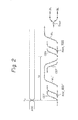
- Figure 2 shows a waveform diagram of an access operation of the device shown in Fig. 1, where a refresh access is carried out when address is changed.
- t F represents a time required for performing a refresh of the memory cells corresponding to a single word line, and the waveforms are shown with respect to a single word line WL', to simplify the explanation.
- CEN is latched in the peripheral circuit 16 during the aforementioned time interval t F and becomes valid after the completion of the refresh operation.
- the subsequent operation is the same as the refresh operation.
- the external access operation is carried out after the completion of the refresh operation. That is, the external access operation is started with a longest delay time t F , from the address changing point.
- Figure 3 shows a waveform diagram of an access operation of the device shown in Fig. 1, where a refresh access or a refresh operation is not carried out when an address is changed.
- the external access operation is carried out at the changing time to of the address signal ADD.
- the row address signals RAN and RAN for external access are output, and then a single word line WL is selected.
- the address signal ADD is generally constituted by a combination of a plurality of address bit signals ADD, -ADD " , for example, as shown in Fig. 4.
- a time lag or lead occurs, i.e., an address skew ASQ among the bit signals, as shown in Fig. 4.
- the external access operation shown in Fig. 3 is normally carried out if the address skew ASQ is within a predetermined range.
- the address skew moves outside the predetermined range, a problem occurs in that another word line different from a word line to be selected is selected. Therefore, the timings of the application of each bit of the address signal must be exactly set.
- this causes another problem, in that the constitution of a device (not shown) supplying the address signal ADD becomes complicated, resulting in a rise in the cost thereof.
- Figure 5 shows another example of a previously-proposed PSRAM device.
- the device shown in Fig. 5 is different from that shown in Fig. 1 in that the ATD circuit 19 in Fig. 1 is replaced by a clock generating circuit 20 which outputs a chip enable signal CEN in response to an external clock, i.e., a low active chip enable signal CE.
- a clock generating circuit 20 which outputs a chip enable signal CEN in response to an external clock, i.e., a low active chip enable signal CE.
- Other arrangements and the operation thereof are the same as those of the device in Fig. 1 and, accordingly, an explanation thereof will be omitted.
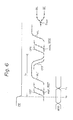
- Figure 6 shows a waveform diagram of an access operation of the device shown in Fig. 5, where a refresh access is carried out when the level of the external clock is changed.
- the mode of operation is the same as that in Fig. 2, but in this case, the external access operation is carried out in accordance with the address information at a time h , to select the word line WL.
- Figure 7 shows a waveform diagram of an access operation of the device shown in Fig. 5, where a refresh access or a refresh operation. is not carried out when the level of the external clock is changed.
- the external access operation is started in response to a change in the external clock CE of from high level to low level, i.e., at the time to.
- the address information for selecting the word line WL must be preset, that it can be determined at a time t 2 prior to the time to.
- the timing of the application of the address signal ADD must be strictly set in association with the timing of the application of the external clock CE. This means that the constitution of a device (not shown) supplying the signals ADD and ⁇ E becomes complicated and the cost thereof is increased, as in Fig. 1.
- Figure 8 shows a block diagram of a PSRAM device embodying one aspect of the present invention.
- reference 30 denotes a memory cell array having a dynamic type memory cell MC consisting of one transistor Q and one capacitor C provided at each intersection between a plurality of word lines and a plurality of bit lines. In the illustrated constitution, only a single memory cell is shown, to simplify the explanation.
- Reference 31 denotes a word decoder which selects the word line WL connected to the memory cell MC based on row address signals RA and RA
- reference 32 denotes a column decoder which selects via a column gate 33 the bit line BL connected to the memory cell MC based on column address signals CA and CA.
- the column gate 33 is opened, and thus the data in the memory cell MC can be read through a data bus DB and an I/O gate 34 to the external, or the data from the external can be written or re-written into the cell in response to a low active write enable signal WE.
- Reference 35 denotes a peripheral circuit for column access which outputs the column address signals CA and CA in response to an address signal ADD and a delayed chip enable signal CEND
- reference 36 denotes a peripheral circuit for row access which outputs row address signals RAN and RAN in response to the signal ADD and the signal CEND.
- the address signals RAN and RAN are input to an arbiter 37, and the address signals CA and CA are input to the column decoder 32.
- Reference 38 denotes a timer which generates a refresh enable signal CEF for performing a refresh of the memory cells corresponding to one word line at a predetermined time interval
- reference 39 denotes a peripheral circuit for a refresh which outputs refresh address signals RAF and RAF in response to the refresh enable signal CEF
- reference 40 denotes a gate circuit connected between the timer 38 and the peripheral circuit 39, and controlling the transmission of the refresh enable signal CEF to the peripheral circuit 39 in response to a chip enable signal CEN.
- the gate circuit 40 transmits the refresh enable signal CEF when the signal CEF is input prior to the chip enable signal CEN, and prohibits the transmission until an external address access based on the chip enable signal CEN is completed, when the signal CEN is input prior to the refresh enable signal CEF.
- the peripheral circuit 39 includes an address counter (not shown) which performs a sequentially renewal of addresses of the word lines based on the signal CEF from the timer 38. Thus, a sequential access to a plurality of word lines is carried out.
- the timer 38, peripheral circuit 39 and gate circuit 40 constitute an internal refresh circuit.
- the arbiter 37 selects either the address signals RAF and RAF from the peripheral circuit 39 for refresh and the address signals RAN and
- Reference 41 denotes an ATD circuit which outputs the chip enable signal CEN in response to a change in address of the address signal ADD
- reference 42 denotes a delay circuit for delaying the chip enable signal CEN by a predetermined time to form a delay signal CEN'
- reference 43 denotes an address comparison circuit which receives the address signal ADD, the chip enable signal CEN from the ATD circuit 41, and the delay signal CEN' from the delay circuit 42.
- the address comparison circuit 43 retains an address information corresponding to the chip enable signal CEN upon receipt of the signal CEN, and retains an address information corresponding to the delay signal CEN' upon receipt of the signal CEN', compares the address information of both, and outputs the delayed control signal CEND when the address information of both are in accord. Namely, the delayed control signal CEND is generated when a change does not occur in the information of the address signal ADD during the time from the generation of the signal CEN to the generation of the signal CEN'.
- the time required for the generation of the delayed control signal CEND after the generation of the chip enable signal CEN is made equal to the time required for carrying out the refresh of the memory cells corresponding to one word line.
- the delayed control signal CEND is supplied to the word decoder 31, column decoder 32, column gate 33, I/0 gate 34, peripheral circuit 35 for column access, and peripheral circuit 36 for row access. Note, where the address information of both based on the signals CEN and CEN' are not in accord, the generation of the signal CEND is inhibited until the address information of both are in accord.
- Figure 9 illustrates a circuit constitution of a part of the arbiter 37 shown in Fig. 8. The circuit in Fig. 9 is shown with respect to one address bit of the address signal.
- a pair of complementary address bits RAF, and RAF, of the refresh address signal are input to one input end of AND gates 51 and 52, respectively, and the refresh enable signal CEF is input to another input end of each of the AND gates 51 and 52.
- Reference 53 denotes a tristate buffer, which prohibits the transmission of the signal output from the AND gate 51, i.e., the address bit signal RAF 1 , in response to the delayed control signal CEND.
- reference 54 denotes a tristate buffer, which prohibits the transmission of the address bit signal RAF 1 , in response to the signal CEND.
- a pair of complementary address bits RANi and RAN, of the row address signal are input to one input end of AND gates 55 and 56, respectively, and the delayed control signal CEND is input to another input end of each of AND gates 55 and 56.
- Reference 57 denotes a tristate buffer, which prohibits the transmission of the address bit signal RAN 1 , in response to the refresh enable signal CEF.
- reference 58 denotes a tristate buffer, which prohibits the transmission of the address bit signal RAN, , in response to the signal CEF.
- the arbiter selects the refresh address bits RAF 1 and RAF, as the access address bits RA 1 and RA 1 when the refresh enable signal CEF is input prior to the delayed control signal CEND. Conversely, when the signal CEND is input prior to the signal CEF, the arbiter selects the row address bits RAN, and RAN, as the access address bits RA 1 and RA 1 .
- Figure 10 shows a waveform diagram of an example of the access operation of the device shown in Fig. 8, where a refresh access or a refresh operation is not carried out when an address is changed.
- the delay circuit 42 delays the chip enable signal CEN by a predetermined time to form the delay signal CEN'. Since the address signal ADD is not changed during the time from the generation of the signal CEN to the generation of the signal CEN', the delayed control signal CEND is output from the address comparison circuit 43.
- the peripheral circuits 35 and 36 output the column address signals CA, CA (not shown) and the row address signals RAN, RAN, respectively.
- the row address signals RAN, RAN are fed via the arbiter 37 to the word decoder 31 as the signals RA, RA.
- Each circuit indicated by references 31 to 34 operates, in response to the delayed control signal CEND, and thus the address access is carried out.
- the potential on the word line WL rises to a predetermined level, the data in the corresponding memory cell is read to the bit lines BL and BL.
- the external access operation is carried out after the completion of the refresh operation. In this case, however, the external access operation is started at a time delayed from the time to by the time t F , not immediately after the completion of the refresh operation.
- the refresh operation takes precedence over the external access operation.
- the external access operation is started.
- the problem due to an address skew at the address change e.g., an incorrect selection of a word line
- a sufficient time t F is given as the time interval from the time of the address change to the time of the actual address access.
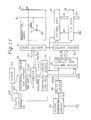
- FIG. 11 shows a block diagram of a PSRAM device embodying another aspect of the present invention.
- the constitution of the device in Fig. 11 is almost the same as that in Fig. 8 except that the ATD circuit 41, delay circuit 42 and address comparison circuit 43 employed in the device in Fig. 8, are replaced by a clock generating circuit 44 for outputting the chip enable signal CEN in response to a low active chip enable signal CE and a delay circuit 45 for delaying the signal CEN by the predetermined time t F , and feeding the delayed signal to the peripheral circuits 35 and 36 as the delayed control signal CEND.
- Other arrangements and the operation of the device in Fig. 11 are the same as those in the device in Fig. 8 and, accordingly, an explanation thereof will be omitted.
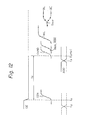
- Figure 12 shows a waveform diagram of an example of the access operation of the device shown in Fig. 11, where a refresh access or a refresh operation is not carried out when the level of an external clock CE is changed.
- the chip enable signal CEN is generated in response to a change from high level to low level of the external clock CE, i.e., at the time to , preparation for the external access operation is made.
- the gate circuit 40 is closed in response to the signal CEN, and thus the refresh access is prohibited.
- the delay circuit 45 delays the signal CEN by the predetermined time t F , i.e., the time required for performing a refresh of the memory cells corresponding to one word line, and outputs the delayed signal as the delayed control signal CEND.
- Each circuit indicated by references 31 to 36 operates in response to the signal CEND, and thus the address access is carried out.
- the column address signals CA, CA (not shown) and the row address signals RAN, RAN are output and the potential on the word line WL rises, and as a result, the data in the corresponding memory cell is read to the bit lines BL and BL
- the time t 3 of the address change in the address single ADD can be arbitrarily set within the range between the time to and the time (to + t F ), because sufficient time t F Î S assured as the time interval from the time of the change in the level of the clock CE to the time of the actual address access.
- the previously-proposed PSRAM device shown by a broken line
- CE or the access operation where the refresh access is carried out some time prior to the time to , is the same as that of the device in Fig. 8, and thus an explanation thereof will be omitted.
Landscapes
- Engineering & Computer Science (AREA)
- Computer Hardware Design (AREA)
- Microelectronics & Electronic Packaging (AREA)
- Dram (AREA)
Applications Claiming Priority (2)
| Application Number | Priority Date | Filing Date | Title |
|---|---|---|---|
| JP301606/86 | 1986-12-19 | ||
| JP61301606A JPS63155494A (ja) | 1986-12-19 | 1986-12-19 | 擬似スタテイツクメモリ装置 |
Publications (3)
| Publication Number | Publication Date |
|---|---|
| EP0273652A2 true EP0273652A2 (de) | 1988-07-06 |
| EP0273652A3 EP0273652A3 (en) | 1990-06-13 |
| EP0273652B1 EP0273652B1 (de) | 1993-09-29 |
Family
ID=17898971
Family Applications (1)
| Application Number | Title | Priority Date | Filing Date |
|---|---|---|---|
| EP87311150A Expired - Lifetime EP0273652B1 (de) | 1986-12-19 | 1987-12-17 | Pseudostatische Speichereinrichtung mit einer internen Selbstauffrischungsschaltung |
Country Status (4)
| Country | Link |
|---|---|
| US (1) | US4809233A (de) |
| EP (1) | EP0273652B1 (de) |
| JP (1) | JPS63155494A (de) |
| KR (1) | KR920001758B1 (de) |
Cited By (7)
| Publication number | Priority date | Publication date | Assignee | Title |
|---|---|---|---|---|
| EP0980076A3 (de) * | 1998-08-11 | 2001-04-25 | Infineon Technologies North America Corp. | Verfahren und Anordnungen zum Aktivieren eines Speichers |
| WO2001041149A1 (en) * | 1999-12-03 | 2001-06-07 | Nec Corporation | Semiconductor storage and method for testing the same |
| EP1204118A3 (de) * | 2000-11-06 | 2003-05-14 | Fujitsu Limited | Halbleiterspeicheranordnung mit SRAM Schnittstellevorrichtung |
| US6643732B1 (en) * | 2001-11-14 | 2003-11-04 | Etron Technology, Inc. | Delayed read/write scheme for SRAM interface compatible DRAM |
| EP1248266A3 (de) * | 2001-04-06 | 2004-06-23 | Fujitsu Limited | Steuerungsschaltung und Halbleiterspeicheranordnung |
| EP1394806A3 (de) * | 2002-08-28 | 2004-07-14 | Fujitsu Limited | Halbleiterspeicheranordnung |
| US7006401B2 (en) | 2001-12-27 | 2006-02-28 | Nec Electronics Corp. | Semiconductor storage device and refresh control method thereof |
Families Citing this family (25)
| Publication number | Priority date | Publication date | Assignee | Title |
|---|---|---|---|---|
| JPS62188095A (ja) * | 1986-02-14 | 1987-08-17 | Toshiba Corp | 半導体記憶装置の制御回路 |
| JPS63121197A (ja) * | 1986-11-07 | 1988-05-25 | Fujitsu Ltd | 半導体記憶装置 |
| US4870616A (en) * | 1987-09-29 | 1989-09-26 | Maryland | Compact register set using a psram array |
| FR2623653B1 (fr) * | 1987-11-24 | 1992-10-23 | Sgs Thomson Microelectronics | Procede de test de cellules de memoire electriquement programmable et circuit integre correspondant |
| JP2534757B2 (ja) * | 1988-07-06 | 1996-09-18 | 株式会社東芝 | リフレッシュ回路 |
| JPH0221490A (ja) * | 1988-07-07 | 1990-01-24 | Oki Electric Ind Co Ltd | ダイナミック・ランダム・アクセス・メモリ |
| JPH0261894A (ja) * | 1988-08-25 | 1990-03-01 | Nec Ic Microcomput Syst Ltd | 非同期式メモリ |
| KR940008147B1 (ko) * | 1991-11-25 | 1994-09-03 | 삼성전자 주식회사 | 저전력 데이타 리텐션 기능을 가지는 반도체 메모리장치 |
| US5617551A (en) * | 1992-09-18 | 1997-04-01 | New Media Corporation | Controller for refreshing a PSRAM using individual automatic refresh cycles |
| KR100276386B1 (ko) * | 1997-12-06 | 2001-01-15 | 윤종용 | 반도체메모리장치의리프레시방법및회로 |
| US6606267B2 (en) * | 1998-06-23 | 2003-08-12 | Sandisk Corporation | High data rate write process for non-volatile flash memories |
| CN100541657C (zh) * | 1999-12-03 | 2009-09-16 | 恩益禧电子股份有限公司 | 存储装置及等待控制电路 |
| KR100384057B1 (ko) * | 2000-06-29 | 2003-05-16 | 삼성전자주식회사 | 어드레스 스큐 프리회로를 가지는 반도체 메모리 장치 |
| JP2003059264A (ja) * | 2001-08-08 | 2003-02-28 | Hitachi Ltd | 半導体記憶装置 |
| KR100437607B1 (ko) * | 2001-09-14 | 2004-06-30 | 주식회사 하이닉스반도체 | 반도체 메모리 장치의 리프레쉬 발생회로 |
| KR100599411B1 (ko) * | 2001-10-23 | 2006-07-10 | 주식회사 코아매직 | 스토리지 커패시터를 포함하는 셀을 가지는 에스램 및 그라이트데이타 입력방법 |
| US6798711B2 (en) * | 2002-03-19 | 2004-09-28 | Micron Technology, Inc. | Memory with address management |
| US6920524B2 (en) * | 2003-02-03 | 2005-07-19 | Micron Technology, Inc. | Detection circuit for mixed asynchronous and synchronous memory operation |
| US7042777B2 (en) * | 2004-01-28 | 2006-05-09 | Infineon Technologies Ag | Memory device with non-variable write latency |
| US7042786B2 (en) * | 2004-04-26 | 2006-05-09 | Infineon Technologies Ag | Memory with adjustable access time |
| US7167400B2 (en) * | 2004-06-22 | 2007-01-23 | Micron Technology, Inc. | Apparatus and method for improving dynamic refresh in a memory device |
| JP2006092640A (ja) * | 2004-09-24 | 2006-04-06 | Sanyo Electric Co Ltd | メモリ |
| KR100689863B1 (ko) * | 2005-12-22 | 2007-03-08 | 삼성전자주식회사 | 반도체 메모리 장치 및 그에 따른 방법 |
| DE102006062666A1 (de) | 2006-12-29 | 2008-07-03 | Samsung Electronics Co., Ltd., Suwon | Halbleiterspeicherbauelement und Zugriffs- und Auffrischungsverfahren |
| TWI498890B (zh) * | 2012-08-10 | 2015-09-01 | Etron Technology Inc | 偽靜態隨機存取記憶體之運作方法及相關記憶裝置 |
Family Cites Families (6)
| Publication number | Priority date | Publication date | Assignee | Title |
|---|---|---|---|---|
| US4337525A (en) * | 1979-04-17 | 1982-06-29 | Nippon Electric Co., Ltd. | Asynchronous circuit responsive to changes in logic level |
| US4360903A (en) * | 1980-09-10 | 1982-11-23 | Mostek Corporation | Clocking system for a self-refreshed dynamic memory |
| JPH0762958B2 (ja) * | 1983-06-03 | 1995-07-05 | 株式会社日立製作所 | Mos記憶装置 |
| JP2518810B2 (ja) * | 1983-11-29 | 1996-07-31 | 富士通株式会社 | 半導体集積回路装置 |
| US4764901A (en) * | 1984-08-03 | 1988-08-16 | Kabushiki Kaisha Toshiba | Semiconductor memory device capable of being accessed before completion of data output |
| JPS61265796A (ja) * | 1985-05-20 | 1986-11-25 | Nec Ic Microcomput Syst Ltd | 半導体記憶装置 |
-
1986
- 1986-12-19 JP JP61301606A patent/JPS63155494A/ja active Pending
-
1987
- 1987-12-17 EP EP87311150A patent/EP0273652B1/de not_active Expired - Lifetime
- 1987-12-18 US US07/135,102 patent/US4809233A/en not_active Expired - Fee Related
- 1987-12-19 KR KR1019870014567A patent/KR920001758B1/ko not_active Expired
Cited By (11)
| Publication number | Priority date | Publication date | Assignee | Title |
|---|---|---|---|---|
| EP0980076A3 (de) * | 1998-08-11 | 2001-04-25 | Infineon Technologies North America Corp. | Verfahren und Anordnungen zum Aktivieren eines Speichers |
| WO2001041149A1 (en) * | 1999-12-03 | 2001-06-07 | Nec Corporation | Semiconductor storage and method for testing the same |
| US6751144B2 (en) | 1999-12-03 | 2004-06-15 | Nec Electronics Corporation | Semiconductor storage and method for testing the same |
| CN100342455C (zh) * | 1999-12-03 | 2007-10-10 | 恩益禧电子股份有限公司 | 半导体存储装置及其测试方法 |
| EP1204118A3 (de) * | 2000-11-06 | 2003-05-14 | Fujitsu Limited | Halbleiterspeicheranordnung mit SRAM Schnittstellevorrichtung |
| EP1248266A3 (de) * | 2001-04-06 | 2004-06-23 | Fujitsu Limited | Steuerungsschaltung und Halbleiterspeicheranordnung |
| EP1667162A1 (de) * | 2001-04-06 | 2006-06-07 | Fujitsu Limited | Steuerschaltung und Halbleiterspeicherelement |
| US6643732B1 (en) * | 2001-11-14 | 2003-11-04 | Etron Technology, Inc. | Delayed read/write scheme for SRAM interface compatible DRAM |
| US7006401B2 (en) | 2001-12-27 | 2006-02-28 | Nec Electronics Corp. | Semiconductor storage device and refresh control method thereof |
| EP1394806A3 (de) * | 2002-08-28 | 2004-07-14 | Fujitsu Limited | Halbleiterspeicheranordnung |
| KR100826549B1 (ko) | 2002-08-28 | 2008-05-02 | 후지쯔 가부시끼가이샤 | 반도체 기억 장치 |
Also Published As
| Publication number | Publication date |
|---|---|
| EP0273652A3 (en) | 1990-06-13 |
| KR880008327A (ko) | 1988-08-30 |
| EP0273652B1 (de) | 1993-09-29 |
| JPS63155494A (ja) | 1988-06-28 |
| KR920001758B1 (ko) | 1992-02-24 |
| US4809233A (en) | 1989-02-28 |
Similar Documents
| Publication | Publication Date | Title |
|---|---|---|
| US4809233A (en) | Pseudo-static memory device having internal self-refresh circuit | |
| EP0563082B1 (de) | Synchrone auffrischung eines dynamischen ram-speichers | |
| US7778099B2 (en) | Semiconductor memory, memory system, and memory access control method | |
| US5703813A (en) | DRAM having multiple column address strobe operation | |
| US6741515B2 (en) | DRAM with total self refresh and control circuit | |
| US5999481A (en) | Method and apparatus for controlling the operation of an integrated circuit responsive to out-of-synchronism control signals | |
| US4691303A (en) | Refresh system for multi-bank semiconductor memory | |
| EP0955640A2 (de) | Dekodierter Selbstauffrischungsmode für DRAM | |
| US6463005B2 (en) | Semiconductor memory device | |
| US5185719A (en) | High speed dynamic, random access memory with extended reset/precharge time | |
| US5367493A (en) | Dynamic type semiconductor memory device having reduced peak current during refresh mode and method of operating the same | |
| US6456563B1 (en) | Semiconductor memory device that operates in sychronization with a clock signal | |
| US20020191479A1 (en) | Semiconductor memory device operable for both of CAS latencies of one and more than one | |
| US6026041A (en) | Semiconductor memory device | |
| US7042777B2 (en) | Memory device with non-variable write latency | |
| US20020001254A1 (en) | Synchronous semiconductor memory device | |
| US7072228B2 (en) | Semiconductor memory device with improved precharge timing | |
| CA1039851A (en) | Timing control in semiconductor memory systems | |
| US4901282A (en) | Power efficient static-column DRAM | |
| US6122214A (en) | Semiconductor memory | |
| JPH0325871B2 (de) | ||
| KR19980040799A (ko) | 반도체 메모리 장치의 자동 프리차아지 신호 발생회로 | |
| EP0468135B1 (de) | Dynamischer wahlfreier Speicher mit hoher Geschwindigkeit und verlängerter Rückstell-/Vorladezeit | |
| US6845056B2 (en) | Semiconductor memory device with reduced power consumption | |
| KR100238236B1 (ko) | 반도체 메모리장치의 셀프 리프레쉬 방법 |
Legal Events
| Date | Code | Title | Description |
|---|---|---|---|
| PUAI | Public reference made under article 153(3) epc to a published international application that has entered the european phase |
Free format text: ORIGINAL CODE: 0009012 |
|
| AK | Designated contracting states |
Kind code of ref document: A2 Designated state(s): DE FR GB |
|
| PUAL | Search report despatched |
Free format text: ORIGINAL CODE: 0009013 |
|
| AK | Designated contracting states |
Kind code of ref document: A3 Designated state(s): DE FR GB |
|
| 17P | Request for examination filed |
Effective date: 19901017 |
|
| 17Q | First examination report despatched |
Effective date: 19911010 |
|
| RBV | Designated contracting states (corrected) |
Designated state(s): FR |
|
| REG | Reference to a national code |
Ref country code: DE Ref legal event code: 8566 |
|
| GRAA | (expected) grant |
Free format text: ORIGINAL CODE: 0009210 |
|
| AK | Designated contracting states |
Kind code of ref document: B1 Designated state(s): FR |
|
| PG25 | Lapsed in a contracting state [announced via postgrant information from national office to epo] |
Ref country code: FR Effective date: 19930929 |
|
| EN | Fr: translation not filed | ||
| PLBE | No opposition filed within time limit |
Free format text: ORIGINAL CODE: 0009261 |
|
| STAA | Information on the status of an ep patent application or granted ep patent |
Free format text: STATUS: NO OPPOSITION FILED WITHIN TIME LIMIT |
|
| 26N | No opposition filed |