EP0273743A2 - Elektronisches Bauelement mit einem Elektroden- und Steuerschaltungssubstrat für Anzeigetafeln - Google Patents
Elektronisches Bauelement mit einem Elektroden- und Steuerschaltungssubstrat für Anzeigetafeln Download PDFInfo
- Publication number
- EP0273743A2 EP0273743A2 EP87311454A EP87311454A EP0273743A2 EP 0273743 A2 EP0273743 A2 EP 0273743A2 EP 87311454 A EP87311454 A EP 87311454A EP 87311454 A EP87311454 A EP 87311454A EP 0273743 A2 EP0273743 A2 EP 0273743A2
- Authority
- EP
- European Patent Office
- Prior art keywords
- film
- alloy
- tantalum
- molybdenum
- electronic device
- Prior art date
- Legal status (The legal status is an assumption and is not a legal conclusion. Google has not performed a legal analysis and makes no representation as to the accuracy of the status listed.)
- Withdrawn
Links
Images





Classifications
-
- H—ELECTRICITY
- H10—SEMICONDUCTOR DEVICES; ELECTRIC SOLID-STATE DEVICES NOT OTHERWISE PROVIDED FOR
- H10D—INORGANIC ELECTRIC SEMICONDUCTOR DEVICES
- H10D30/00—Field-effect transistors [FET]
- H10D30/60—Insulated-gate field-effect transistors [IGFET]
- H10D30/67—Thin-film transistors [TFT]
- H10D30/6729—Thin-film transistors [TFT] characterised by the electrodes
- H10D30/6737—Thin-film transistors [TFT] characterised by the electrodes characterised by the electrode materials
- H10D30/6739—Conductor-insulator-semiconductor electrodes
-
- H—ELECTRICITY
- H10—SEMICONDUCTOR DEVICES; ELECTRIC SOLID-STATE DEVICES NOT OTHERWISE PROVIDED FOR
- H10D—INORGANIC ELECTRIC SEMICONDUCTOR DEVICES
- H10D84/00—Integrated devices formed in or on semiconductor substrates that comprise only semiconducting layers, e.g. on Si wafers or on GaAs-on-Si wafers
- H10D84/01—Manufacture or treatment
-
- H—ELECTRICITY
- H10—SEMICONDUCTOR DEVICES; ELECTRIC SOLID-STATE DEVICES NOT OTHERWISE PROVIDED FOR
- H10D—INORGANIC ELECTRIC SEMICONDUCTOR DEVICES
- H10D86/00—Integrated devices formed in or on insulating or conducting substrates, e.g. formed in silicon-on-insulator [SOI] substrates or on stainless steel or glass substrates
- H10D86/40—Integrated devices formed in or on insulating or conducting substrates, e.g. formed in silicon-on-insulator [SOI] substrates or on stainless steel or glass substrates characterised by multiple TFTs
-
- H—ELECTRICITY
- H10—SEMICONDUCTOR DEVICES; ELECTRIC SOLID-STATE DEVICES NOT OTHERWISE PROVIDED FOR
- H10D—INORGANIC ELECTRIC SEMICONDUCTOR DEVICES
- H10D86/00—Integrated devices formed in or on insulating or conducting substrates, e.g. formed in silicon-on-insulator [SOI] substrates or on stainless steel or glass substrates
- H10D86/40—Integrated devices formed in or on insulating or conducting substrates, e.g. formed in silicon-on-insulator [SOI] substrates or on stainless steel or glass substrates characterised by multiple TFTs
- H10D86/441—Interconnections, e.g. scanning lines
-
- H—ELECTRICITY
- H10—SEMICONDUCTOR DEVICES; ELECTRIC SOLID-STATE DEVICES NOT OTHERWISE PROVIDED FOR
- H10D—INORGANIC ELECTRIC SEMICONDUCTOR DEVICES
- H10D86/00—Integrated devices formed in or on insulating or conducting substrates, e.g. formed in silicon-on-insulator [SOI] substrates or on stainless steel or glass substrates
- H10D86/40—Integrated devices formed in or on insulating or conducting substrates, e.g. formed in silicon-on-insulator [SOI] substrates or on stainless steel or glass substrates characterised by multiple TFTs
- H10D86/60—Integrated devices formed in or on insulating or conducting substrates, e.g. formed in silicon-on-insulator [SOI] substrates or on stainless steel or glass substrates characterised by multiple TFTs wherein the TFTs are in active matrices
-
- H—ELECTRICITY
- H10—SEMICONDUCTOR DEVICES; ELECTRIC SOLID-STATE DEVICES NOT OTHERWISE PROVIDED FOR
- H10P—GENERIC PROCESSES OR APPARATUS FOR THE MANUFACTURE OR TREATMENT OF DEVICES COVERED BY CLASS H10
- H10P14/00—Formation of materials, e.g. in the shape of layers or pillars
- H10P14/60—Formation of materials, e.g. in the shape of layers or pillars of insulating materials
- H10P14/69—Inorganic materials
- H10P14/692—Inorganic materials composed of oxides, glassy oxides or oxide-based glasses
- H10P14/6938—Inorganic materials composed of oxides, glassy oxides or oxide-based glasses the material containing at least one metal element, e.g. metal oxides, metal oxynitrides or metal oxycarbides
- H10P14/6939—Inorganic materials composed of oxides, glassy oxides or oxide-based glasses the material containing at least one metal element, e.g. metal oxides, metal oxynitrides or metal oxycarbides characterised by the metal
- H10P14/69396—Inorganic materials composed of oxides, glassy oxides or oxide-based glasses the material containing at least one metal element, e.g. metal oxides, metal oxynitrides or metal oxycarbides characterised by the metal the material containing at least one rare earth metal element, e.g. oxides of lanthanides, scandium or yttrium
Definitions
- the present invention relates to an electronic device having an electrode and to a driving circuit substrate for display device.
- an active matrix type liquid crystal display device having a switching element at each picture elements is utilized for a liquid crystal display device.
- the nonlinear elements of TFT (Thin-Film-Transistor), MIM (Metal-Insulator-Metal structure) and the like are utilized for increasing the effective duty ratio of the voltage applied to each picture element.
- As an insulating film for these thin film electron devices a tantalum oxide film (TaO x ) and multi-layered structure of a tantalum oxide film and silicon oxide film (TaO x /SiO x ) are known (Proceedings of "Eurodisplay '81", pp. 220 ⁇ 223).
- the TFT and MIM elements using the tantalum oxide film have a large leak electric current because of the small resistivity of the tantalum oxide film.
- the driving voltage can not be increased sufficiently due to the small breakdown electric field of the tantalum oxide film, and therefore the ON current available for the TFT is limited.
- An object of the present invention is to provide an electronic device using a high resistivity oxide film of an alloy as an insulating film. Another object of the present invention is to provide a driving circuit substrate for a display device using a high resistivity oxide film of the alloy as an insulating film.
- this object of the present invention is accomplished by the electronic device and the driving circuit substrate for a display device using an oxide film of a molybdenum-tantalum alloy having a tantalum composition ratio of 50 to 97 atomic percent.
- an electronic device and a driving circuit substrate for a display device are provided which are characterized by using an oxide film of an Mo-Ta alloy with a Ta composition range of 50 to 97 atomic percent as an insulating material.
- an oxide film of an Mo-Ta alloy is employed as an insulating material of a TFT with the use of an a-Si (amorphous Si) film or as its drain and source electrodes and as a gate electrode interconnection material over a single crystalline silicon substrate, noting that the Ta composition ratio is 50 to 97 atomic percent.
- a total amount of the Mo and Ta may be within a range of above 95 atomic percent in which case the other materials may be contained in a range of less than 5 atomic percent, such as carbon, oxygen, argon, hydrogen and nitrogen.
- the Mo-Ta alloy is smaller in resistivity than those metals such as Ta, Ti and even smaller than MoSi2.
- Respective electrode interconnection films are formed at room temperature by virtue of a sputtering method.
- a sputtering method As evident from Table an Mo-Ta alloy film, after deposited at room temperature, reveals a smaller resistivity than those of Ti, Cr, ⁇ -Ta and MoSi2 films and, for less than 84 atomic percent of Ta in particular, than an Mo film.
- the alloy film when heat-treated after that deposition step, manifests a still lower resistivity. Furthermore, the alloy film also shows an excellent dry-etching workability as in the case of an MoSi2 film and allows a ready formation of a taper. No better thermally oxidized film is obtained for the Mo, Ti and Cr film.
- the Mo-Ta alloy film having a Ta composition ratio of more than 30 atomic percent shows an excellent thermal oxidation and, in addition, an excellent resistance to a mixture solution of H2SO4 and H2O2 which has extensively been used as a washing liquid. It has further been found that the alloy film has a better compatibility with an Si-used semiconductor device due to its excellent ohmic contact with Si and its low reactivity with an SiO2.
- Fig. 1 shows a comparison in resistivity between an Mo-Ta alloy film formed as a single-layered film on a glass substrate by a sputtering method and a multi-layered film with an Mo-Ta alloy film formed on an underlying Mo film.
- the composition ratio of Ta exceeds 84 atomic percent for the single-layered film, the resistivity increases abruptly.
- the composition ratio of Ta is increased (to more than 84 atomic percent) for a multi-layered film, the resistivity is not increased. This is a marked difference upon comparison with the single-layered film.
- the film may be formed by the sputtering method, as well as by, for example, an electron beam evaporation method. Since the underlying metal film primarily determines the crystal structure of the overlying Mo-Ta alloy film, it is only necessary for the underlying metal film to have a thickness of nearly above 100 ⁇ . As the body-centered cubic lattice type metal, use may be made of V, Cr, Fe, Nb, Mo and W whose lattice constant is similar to that of Mo and Ta, as well as an Mo-Ta alloy whose Ta composition ratio is within a range of 0 to 84 atomic percent.
- An anodized film is formed on the surface of the Mo-Ta alloy films, noting that the anodic oxidation was conducted in 0.01 wt% citric acid solution at a temperature ranging from room temperature to 70°C. And the anodic oxidation was conducted at a current density of 0.5 mA/cm2 up to 100 V as a constant-current oxidation. Then the anodic oxidation is continued at 100 V for one hour as a constant-voltage oxidation.
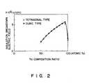
- Fig. 2 shows the connection reference of the insulation breakdown electric field of the resultant Mo-Ta alloy oxidation films.
- Fig. 3 shows the resistivity of the resultant Mo-Ta alloy oxidation films measured with a bias of 30 V.
- the Mo-Ta alloy oxidized film reveals a high insulation breakdown electric field and a high resistivity.
- the dielectric constant of the Mo-Ta alloy oxidation film of this invention is about 30 at the frequency range from 10 kHz to 1 MHz.
- the Mo-Ta alloy whose tantalum composition is more than 84 atomic percent has two kinds of crystalline structures, a tetragonal type and cubic type. However, the characteristics of oxidized film of Mo-Ta alloy with those two kinds of crystalline structures make no difference.
- Fig. 4 is an equivalent circuit diagram showing an interconnection material of this invention as applied to an active matrix type liquid crystal display device using an inverted staggered type TFT.
- Address lines 11 (111, 112, ..., 11 m ) and data lines 13 (131, 132, ..., 13 n ) are arranged as a matrix array on glass substrate 1 with TFT 15 (1511, ..., 15 mn ) placed in a corresponding intersection.
- Capacitor 23pq though shown in Fig. 4, can be omitted.
- Gate electrode 17pq is formed, in reality, integral with address line 11p.
- Fig. 5 is an enlarged plan view showing one pixel area (2122) in the substrate in Fig. 4.
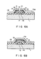
- a liquid crystal display device is manufactured as follows. Reference is invited to Figs. 6A and 6B.
- Figs. 6A and 6B show an embodiment of this invention in which the surface of a gate electrode is anodized.
- Fig. 6A is a cross-sectional view as taken along line A-A ⁇ in Fig. 5
- Fig. 6B is a cross-sectional view as taken along line B-B ⁇ in Fig. 5.
- An Mo-Ta alloy film was deposited by sputtering on glass substrate 1 and the resultant structure was patterned by a PEP (photoengraving process) to form gate electrode 17.
- Gate electrode 17 was formed of the same material as that of address line 11 (See Fig. 1) and formed, by the same process, integral with the address line.
- gate electrode 17 of this embodiment was 200 nm thick and 30 ⁇ m wide, noting that the gate electrode has a thickness the same as that of the address line.
- 61 nm-thick oxidation film 118 was formed on the gate electrode 17 by an anodic oxidation.
- Anodized film 118 was formed on the surface of the resultant structure, noting that the anodic oxidation was conducted in 0.01 wt% citric acid solution at a temperature ranging from room temperature to 70°C.
- the anodized film had a breakdown electric field of above 5.0 ⁇ 106 V/cm and specific dielectric constant of 30.
- 200 nm-thick SiO2 film 132 was formed by a plasma enhanced CVD on the whole surface of the resultant structure.
- 300 nm-thick undoped a-Si film 33, 50 nm-thick n+ type a-Si film 35 and 50 nm-thick Mo film 37 were formed in that order. These three layers were left by etching at the thin-film transistor section and at the respective intersection of address line 11 and data line 13 on address line 11. What is important at this step was a process before gate insulating film 132 was deposited.
- the gate electrode was subjected by PEP to a patterning and a larger amount of organic (the left resist, for example,) and inorganic contaminants were present in the surface of the gate electrode.
- a washing step was carried out by immersing the glass substrate into a mixture solution of H2SO4 and H2O2 with the gate electrode formed on the glass substrate.
- the gate electrode of the alloy film of this invention revealed an adequate corrosion- and etching-resistance to a washing liquid.
- display electrode 21 for the respective pixel was formed by a 150 nm-thick ITO (indium tin oxide) film.
- the resultant structure was subjected to an Al-film deposition and patterning to form data line 13 and continuous source electrode 41 and drain electrode 43.
- Source electrode 41 was formed integral with data line 13 in Fig. 1 to contact with display electrode 21.
- a liquid crystal layer if sandwiched between the active matrix substrate and opposite electrode substrate, provides a liquid crystal display device.
- the SiO2 film is deposited to provide a gate insulating film, it is possible to effectively prevent such a defect resulting from the layer-to-layer short-circuiting. Furthermore, the second insulating film can be thinned, thus offering an advantage of lowering the threshold voltage of TFT's.
- Forming an anodic oxidation film on the whole, not to mention the gate electrode area prevents defects resulting from the interlayer short-circuiting at that intersection in particular.
- a good-quality oxide film can be formed by thermally oxidizing the gate electrode and the other surface in an oxygen atmosphere, for example, for one hour at an atmospheric pressure and 400°C.
- a thin-film transistor was formed with anodized film 118 and SiO2 film 132 as a gate insulating film.
- a multi-layered film of a-Si film 33, n+ type a-Si film 35 and Mo film 37 are formed on an insulating anodized film 118 and SiO2 film 132 to provide an insulating interlayer.
- Fig. 7 shows the characteristics of the relationship between a gate electric field V G and a drain electric current I D of a TFT.
- a solid line shows the characteristic of the TFT using the Mo-Ta alloy film as a gate electrode and the anodized film of the Mo-Ta alloy film as a gate insulating film (Example 1).
- a broken line shows the characteristic of the TFT as a comparative example using a Ta film as a gate electrode and the anodized film of the Ta film as a gate insulating film.
- a dot chain line shows the characteristic of the TFT using the Mo-Ta alloy film as a gate electrode and the anodized film of the Mo-Ta alloy and SiO2 film as a gate insulating film (Example 2).
- the leak current of the drain electric current I D is reduced about 2 figures compared to the comparative example when the gate electric field V G is OFF.
- the drain electric current I D of Example 1 is increased compared to that of Example 2 by reason of the dielectric constant of the Mo-Ta alloy oxidation film of this invention is greater than that of the gate insulating film using SiO2.
- SiO2 film can be deposited on the anodized film, for example by the plasma CVD (Chemical Vapor Deposition).
- Example 2 gate capacity and ON current are reduced due to SiO2 film, but the characteristic of the TFT is good as well as Example 1.
- the breakdown electric field of the gate in Example 1 and 2 is greater than 100 V.
- Fig. 8 shows one embodiment of MIM element of this invention.
- 2500 ⁇ -thick Mo-Ta alloy film 22 having Mo composition ratio of 5 atomic percent and Ta composition ratio of 95 atomic percent is formed on glass substrate 21, then an electrode interconnection is patterned by CDE (Chemical Dry Etching). The contact portion of the electrode interconnection is covered by a photo resist, then anodized film 23 is formed on the surface of Mo-Ta alloy film 22.
- the anodic oxidation was conducted in 0.01 wt% citric acid solution as a constant-current oxidation up to 25 V, then the anodic oxidation is continued at 25 V for one hour as a constant-voltage oxidation.
- One ⁇ m-thick Al film 24 is formed on glass substrate 21 and anodic oxidized film 23, then another electrode connection is formed by patterning.
- Fig. 9 shows the characteristics of the leak electric current I of an MIM shown in Fig. 8 and an MIM element using a Ta and the anodic oxidation film of the Ta. Leak electric current of this example is reduced big as compared to the anodic oxidation of the Ta.
- the alloys to TFT and MIM elements in the above embodiment of this invention may apply to various electronic devices.
- the Mo-Ta alloy film is formed on a metal electrode which has less resistivity such as Cu, Au, Al, and then the oxide film of the Mo-Ta alloy may be formed by an anodic oxidation or thermal oxidation.
- a gate electrode integral with the address line was formed, as multi-layered film of 30 nm-thick Mo-Ta alloy film (80% of Ta) 217a as an underlying metal film and 170 nm-thick Mo-Ta alloy film (95% of Ta) 217b as an overlying metal film, on glass substrate 1. Subsequent to the formation of the gate electrode, washing was carried out in the same way as in the previous embodiment.
- An anodized film 411 and 150 nm-thick SiO2 31 as a gate insulating film were deposited by the CVD method on the surface of the resultant structure.
- Source electrode 41 and drain electrode 43 were formed as an Al layer on the surface of the resultant structure, noting that source electrode 41 was formed integral with data line 13 as set forth above.
- ITO pixel electrode 2122 was formed adjacent to that a-Si film and drain electrode 43 was electrically connected to pixel electrode 2122. In this way a liquid crystal display device was fabricated which had a surface area of 19.2 cm ⁇ 25.6 cm, pixel pitch of 400 ⁇ m and address line of 30 ⁇ m in width.
- address line had a resistance of 12.8 K ⁇ .
- an address line was formed by the other materials and it is found that the resistances of these other materials of Ti, Cr, Mo, Ta and Mo-Ta alloy (60 % of Ta) were 200.5 K ⁇ , 55.4 K ⁇ , 22.6 K ⁇ , 100.9 K ⁇ and 19.2 K ⁇ , respectively.
- an Mo-Ta alloy is obtained by a co-sputtering method with the Mo target and Ta target. It is also possible to obtain a similar alloy film through a thermal decomposition by organic gases containing an Mo and Ta.
- This invention can be applied not only to an Si film, such as an a-Si film, polycrystalline silicon film and single crystalline Si film but also to the other semiconductor material films, such as CdSe, Te, GaAs, and GaP films.
Landscapes
- Liquid Crystal (AREA)
- Thin Film Transistor (AREA)
- Formation Of Insulating Films (AREA)
Applications Claiming Priority (2)
| Application Number | Priority Date | Filing Date | Title |
|---|---|---|---|
| JP61315341A JPS63166236A (ja) | 1986-12-26 | 1986-12-26 | 電子装置 |
| JP315341/86 | 1986-12-26 |
Publications (2)
| Publication Number | Publication Date |
|---|---|
| EP0273743A2 true EP0273743A2 (de) | 1988-07-06 |
| EP0273743A3 EP0273743A3 (de) | 1990-05-02 |
Family
ID=18064243
Family Applications (1)
| Application Number | Title | Priority Date | Filing Date |
|---|---|---|---|
| EP87311454A Withdrawn EP0273743A3 (de) | 1986-12-26 | 1987-12-24 | Elektronisches Bauelement mit einem Elektroden- und Steuerschaltungssubstrat für Anzeigetafeln |
Country Status (3)
| Country | Link |
|---|---|
| EP (1) | EP0273743A3 (de) |
| JP (1) | JPS63166236A (de) |
| KR (1) | KR880008229A (de) |
Cited By (6)
| Publication number | Priority date | Publication date | Assignee | Title |
|---|---|---|---|---|
| FR2631743A1 (fr) * | 1988-05-23 | 1989-11-24 | Gen Electric | Structure a electrodes non coplanaires pour affichage matriciel a cristaux liquides a transistors en couches minces de silicium amorphe et procede de fabrication |
| GB2244858A (en) * | 1990-06-04 | 1991-12-11 | Philips Electronic Associated | MIM type devices for displays |
| US5225364A (en) * | 1989-06-26 | 1993-07-06 | Oki Electric Industry Co., Ltd. | Method of fabricating a thin-film transistor matrix for an active matrix display panel |
| EP0530051A3 (en) * | 1991-08-29 | 1993-09-22 | Sharp Kabushiki Kaisha | A semiconductor device and a method for producing the same |
| GB2314969A (en) * | 1996-07-02 | 1998-01-14 | Lg Electronics Inc | Method of fabricating a thin film transistor |
| WO2006049763A2 (en) | 2004-10-28 | 2006-05-11 | Hewlett-Packard Development Company, L.P. | Thin film semiconductor devices and methods of making |
Families Citing this family (2)
| Publication number | Priority date | Publication date | Assignee | Title |
|---|---|---|---|---|
| JPH022175A (ja) * | 1988-06-14 | 1990-01-08 | Matsushita Electric Ind Co Ltd | 薄膜トランジスタ及びその製造方法 |
| JPH04223334A (ja) * | 1990-12-26 | 1992-08-13 | Matsushita Electric Ind Co Ltd | 絶縁性薄膜 |
Family Cites Families (4)
| Publication number | Priority date | Publication date | Assignee | Title |
|---|---|---|---|---|
| US3754168A (en) * | 1970-03-09 | 1973-08-21 | Texas Instruments Inc | Metal contact and interconnection system for nonhermetic enclosed semiconductor devices |
| FR2530077A1 (fr) * | 1982-07-09 | 1984-01-13 | Radiotechnique Compelec | Procede de realisation de condensateurs integres dans une structure microelectronique |
| JPS60160173A (ja) * | 1984-01-30 | 1985-08-21 | Sharp Corp | 薄膜トランジスタ |
| EP0236629B1 (de) * | 1986-03-06 | 1994-05-18 | Kabushiki Kaisha Toshiba | Steuerschaltung einer Flüssigkristallanzeige |
-
1986
- 1986-12-26 JP JP61315341A patent/JPS63166236A/ja active Pending
-
1987
- 1987-12-24 EP EP87311454A patent/EP0273743A3/de not_active Withdrawn
- 1987-12-26 KR KR870014988A patent/KR880008229A/ko not_active Abandoned
Cited By (13)
| Publication number | Priority date | Publication date | Assignee | Title |
|---|---|---|---|---|
| FR2631743A1 (fr) * | 1988-05-23 | 1989-11-24 | Gen Electric | Structure a electrodes non coplanaires pour affichage matriciel a cristaux liquides a transistors en couches minces de silicium amorphe et procede de fabrication |
| US5225364A (en) * | 1989-06-26 | 1993-07-06 | Oki Electric Industry Co., Ltd. | Method of fabricating a thin-film transistor matrix for an active matrix display panel |
| GB2244858A (en) * | 1990-06-04 | 1991-12-11 | Philips Electronic Associated | MIM type devices for displays |
| EP0530051A3 (en) * | 1991-08-29 | 1993-09-22 | Sharp Kabushiki Kaisha | A semiconductor device and a method for producing the same |
| US5594259A (en) * | 1991-08-29 | 1997-01-14 | Sharp Kabushiki Kaisha | Semiconductor device and a method for producing the same |
| GB2314969B (en) * | 1996-07-02 | 1998-12-02 | Lg Electronics Inc | Method of fabricating a semiconductor device such as a thin film transistor |
| GB2314969A (en) * | 1996-07-02 | 1998-01-14 | Lg Electronics Inc | Method of fabricating a thin film transistor |
| US6107640A (en) * | 1996-07-02 | 2000-08-22 | Lg Electronics Inc. | Semiconductor device for a thin film transistor |
| US6605494B1 (en) | 1996-07-02 | 2003-08-12 | Lg Electronics Inc. | Method of fabricating thin film transistor |
| WO2006049763A2 (en) | 2004-10-28 | 2006-05-11 | Hewlett-Packard Development Company, L.P. | Thin film semiconductor devices and methods of making |
| WO2006049763A3 (en) * | 2004-10-28 | 2006-08-03 | Hewlett Packard Development Co | Thin film semiconductor devices and methods of making |
| US7291522B2 (en) | 2004-10-28 | 2007-11-06 | Hewlett-Packard Development Company, L.P. | Semiconductor devices and methods of making |
| US8823100B2 (en) | 2004-10-28 | 2014-09-02 | Hewlett-Packard Development Company, L.P. | Semiconductor devices and methods of making |
Also Published As
| Publication number | Publication date |
|---|---|
| KR880008229A (ko) | 1988-08-30 |
| JPS63166236A (ja) | 1988-07-09 |
| EP0273743A3 (de) | 1990-05-02 |
Similar Documents
| Publication | Publication Date | Title |
|---|---|---|
| EP0236629B1 (de) | Steuerschaltung einer Flüssigkristallanzeige | |
| EP0430702B1 (de) | Werkstoff für elektrische Leiter, Elektronikagerät welches diesen verwendet und Flüssig-Kristall-Anzeige | |
| US5170244A (en) | Electrode interconnection material, semiconductor device using this material and driving circuit substrate for display device | |
| US4905066A (en) | Thin-film transistor | |
| JP4166105B2 (ja) | 半導体装置およびその製造方法 | |
| EP0457328B1 (de) | Aktive Matrix-Struktur für Flüssig-Kristall-Anzeigeelementen | |
| KR100600229B1 (ko) | 전자 디바이스와 그의 제법, 및 스퍼터링 타겟 | |
| KR101199533B1 (ko) | 식각액, 이를 이용하는 배선 형성 방법 및 박막 트랜지스터기판의 제조 방법 | |
| US5821622A (en) | Liquid crystal display device | |
| US6376861B1 (en) | Thin film transistor and method for fabricating the same | |
| US5334860A (en) | Panel having thin film element formed thereon | |
| US6087730A (en) | Electronic devices and their manufacture | |
| US20100065837A1 (en) | Method for manufacturing thin film transistor using oxide semiconductor and display apparatus | |
| JPH06232129A (ja) | 電子回路 | |
| KR101000451B1 (ko) | Tft lcd 기판의 알루미늄 배선 형성방법과 이에의한 tft lcd 기판 | |
| EP0641028B1 (de) | Dünnfilmanordnung und Verfahren zur Herstellung | |
| US20060283833A1 (en) | Wiring for display device and thin film transistor array panel with the same, and manufacturing method thereof | |
| KR100472175B1 (ko) | 몰리브덴또는몰리브덴합금을이용한반도체장치의제조방법 | |
| EP0329274A1 (de) | Verfahren zur Bildung anodisierter Gebiete auf einer anodisierbaren Metallschicht | |
| JP2585267B2 (ja) | 液晶表示装置 | |
| JP3245613B2 (ja) | 薄膜素子の製造方法 | |
| JP3245612B2 (ja) | 多層配線板の製造方法 | |
| JP3245614B2 (ja) | 薄膜素子の製造方法 | |
| JP3257001B2 (ja) | 多層配線板及び多層配線板の製造方法 | |
| JPH05183162A (ja) | 傾斜機能材料薄膜及び薄膜トランジスタ |
Legal Events
| Date | Code | Title | Description |
|---|---|---|---|
| PUAI | Public reference made under article 153(3) epc to a published international application that has entered the european phase |
Free format text: ORIGINAL CODE: 0009012 |
|
| 17P | Request for examination filed |
Effective date: 19880211 |
|
| AK | Designated contracting states |
Kind code of ref document: A2 Designated state(s): DE FR GB |
|
| PUAL | Search report despatched |
Free format text: ORIGINAL CODE: 0009013 |
|
| AK | Designated contracting states |
Kind code of ref document: A3 Designated state(s): DE FR GB |
|
| 17Q | First examination report despatched |
Effective date: 19910606 |
|
| STAA | Information on the status of an ep patent application or granted ep patent |
Free format text: STATUS: THE APPLICATION IS DEEMED TO BE WITHDRAWN |
|
| 18D | Application deemed to be withdrawn |
Effective date: 19911017 |