EP0274850A2 - Filtres numériques et annuleurs d'écho adaptatifs - Google Patents
Filtres numériques et annuleurs d'écho adaptatifs Download PDFInfo
- Publication number
- EP0274850A2 EP0274850A2 EP87310605A EP87310605A EP0274850A2 EP 0274850 A2 EP0274850 A2 EP 0274850A2 EP 87310605 A EP87310605 A EP 87310605A EP 87310605 A EP87310605 A EP 87310605A EP 0274850 A2 EP0274850 A2 EP 0274850A2
- Authority
- EP
- European Patent Office
- Prior art keywords
- output
- coefficient
- order
- variable
- filter
- Prior art date
- Legal status (The legal status is an assumption and is not a legal conclusion. Google has not performed a legal analysis and makes no representation as to the accuracy of the status listed.)
- Granted
Links
Images






Classifications
-
- H—ELECTRICITY
- H03—ELECTRONIC CIRCUITRY
- H03H—IMPEDANCE NETWORKS, e.g. RESONANT CIRCUITS; RESONATORS
- H03H21/00—Adaptive networks
- H03H21/0012—Digital adaptive filters
-
- H—ELECTRICITY
- H04—ELECTRIC COMMUNICATION TECHNIQUE
- H04B—TRANSMISSION
- H04B3/00—Line transmission systems
- H04B3/02—Details
- H04B3/20—Reducing echo effects or singing; Opening or closing transmitting path; Conditioning for transmission in one direction or the other
- H04B3/23—Reducing echo effects or singing; Opening or closing transmitting path; Conditioning for transmission in one direction or the other using a replica of transmitted signal in the time domain, e.g. echo cancellers
-
- H—ELECTRICITY
- H04—ELECTRIC COMMUNICATION TECHNIQUE
- H04B—TRANSMISSION
- H04B3/00—Line transmission systems
- H04B3/02—Details
- H04B3/20—Reducing echo effects or singing; Opening or closing transmitting path; Conditioning for transmission in one direction or the other
- H04B3/23—Reducing echo effects or singing; Opening or closing transmitting path; Conditioning for transmission in one direction or the other using a replica of transmitted signal in the time domain, e.g. echo cancellers
- H04B3/238—Reducing echo effects or singing; Opening or closing transmitting path; Conditioning for transmission in one direction or the other using a replica of transmitted signal in the time domain, e.g. echo cancellers using initial training sequence
Definitions
- This invention relates to adaptive digital filters capable of generating an arbitrary transfer function having a fast rate of convergence, suitable for use in an echo canceler.
- the adaptive digital filter disclosed therein displays excellent convergence characteristics when the input signal is a white-noise signal.
- the input signal has a non-white characteristic, as in a voice signal, the outputs from each section of the filter are not orthogonal, and their mean square values are unequal, so the convergence characteristics of the variable coefficients are degraded.
- the invention provides an adaptive digital filter comprising M basic sections (wherein M is a positive integer) each having a second order recursive filter with scaler coefficients a m and b m , a first coefficient scaler for multiplying a first output from the second-order recursive filter by a first coefficient, a first variable-coefficient scaler for multiplying the first output from the second-order filter by a first variable-coefficient, a first adder for adding the output from the first scaler and a second output from the second-order recursive filter, a second variable-coefficient scaler for multiplying the output from the first-adder by a second variable-coefficient, and a second adder for adding the outputs from each of the variable coefficient scalers, characterised in that the scaler coefficients a m and b m are selected such that the poles of the second order recursive filter are located near the unit circle in the Z plane, and the first variable-coefficient and the second variable coefficient are selected such that the mean square values of
- first output from the second-order recursive filter is a first-order delayed output and the second output from the second order recursive filter is a zeroth-order delayed output.
- first output from the second order recursive filter is a zeroth order delayed output and the second output from the second order recursive filter is a first order delayed output.
- the M basic sections are preferably connected in series.
- M-1 of the M basic sections mayf have a second order non-recursive filter the output of which is connected to the second order recursive filter of the next section.
- the M basic sections may be connected in parallel.
- the outputs from the second adder of each section may be added to produce the final output from the filter.
- identification means comprise a signal input terminal 11, an error output terminal 12, an unknown system 13, and adaptive digital filter (ADF) 14, and an adder 15.
- x(k) is the input to the unknown system 13 and the adaptive digital filter 14 at time k
- y(k) is the output from the unknown system 13 at time k
- y(k) is the output from the adaptive digital filter 14 at time k
- e(k) is the estimation error at time k
- H(z) is the transfer function of the unknown system
- H (Z) is the transfer function of the adaptive digital filter 14.
- FIG. 2 is a schematic diagram of a teleconferencing system employing an echo canceler.
- This system comprises a pair of microphones 21-1 and 21-2, a pair of loudspeakers 22-1 and 22-2, a pair of echo cancelers 23-1 and 23-2. a pair of transmission lines 24-1 and 24-2, and a pair of adaptive digital filters 25-1 and 25-2, and includes a pair of acoustically coupled paths 26-1 and 26-2.
- the loudspeaker and microphone shown in Figure 2 are integrated into a single unit called a voice terminal. This gives rise to an acoustic coupling between the loudspeaker and the microphone: the signal output from the loudspeaker is coupled into the microphone and greatly degrades the quality of the voice transmission.
- This adaptive digital filter comprises M basic sections connected in series (where M is a positive integer).
- Basic sections 1 through M-1 each comprise a second-order recursive digital filter and a second-order non-recursive digital filter.
- Each basic section also has a first-order non-recursive digital filter comprising a scaler R m for multiplying the first-order delayed output um(k-1) by the coefficient R m , an adder 31 for adding the result to the Oth-order delayed output u m (k), a scaler S m for multiplying the output of the adder 31 m by the coefficient S m , a variable-coefficient scaler C m (k) for multiplying the result u m (k) by a variable coefficent cm(k), a variable-coefficient scaler d m (k) for multiplying the first-order delayed output um(k-1) by a variable coefficient d m (k), and an adder 32 m for adding the outputs of the two variable-coefficient scalers c m (k) and d m (k).
- the outputs from the adders 32 m are added one after the other and the output from the adder 33 M is the output y(k) of the filter with respect to
- the input signal x(k) has a white characteristic
- a circuit with a transfer function F(z) converts this to a signal with a non-white characteristic, which is input to the adaptive digital filter.
- g m (z) and v m (z) be the z-transforms of g m (k) and v m (k).
- the purpose of the variable scaler coefficients A m (k) and B m (k) is to equalize the mean square values of the input signals to the scaler c m (k) with variable scaler coefficient c m (k) and the scaler d m (k) with variable scaler coefficient d m (k).
- a m (k) and B m (k) are accordingly selected as follows:
- f m (z) Z 2 -a m z + b m and a m and b m are selected so that the roots (poles) of f m (z) are located near the unit circle, and the variable scaler coefficients C m and D m are updated by Eqs. (11) and (13), the signals g m (k) and v m (k) will be nearly orthogonal and their mean square values will all be equal; therefore the rate of convergence of the adaptive parameters will be extremely fast.
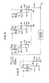
- FIG. 7 shows a first embodiment based on the principles above.
- the adaptive digital filter used in this embodiment comprises M basic sections connected in series (where M is a positive integer).
- the first M-1 basic sections (from 1 to M - 1) each comprises a second-order recursive digital filter and a second-order non-recursive digital filter.
- the final basic section (M) comprises a second-order recursive digital filter.
- the output of the second-order non-recursive digital filter is connected to the input of the second-order recursive digital filter in the next section.
- An adder 3 m +1 adds the output of the second adder 2 m to the output of the second adder 2 m-1 in the next section, and this process continues through the adder 3 M , from which is obtained the final output y(k) of the filter.
- the scaler coefficents a m and b m are selected as described above. Specifically, they are determined as follows. If a m and b m are selected so that:
- N(z) is a function of C m and D m . If R « 1, then H(Z) ⁇ N(z), so that the unknown system can be estimated to be N(z).
- the output signal from F(z), which becomes the input to the first basic section, is added to the output of the second-order recursive digital filter in that section.
- the sum, which is the Oth-order delayed output, is multiplied by the coefficient bi.
- the result is added to the output of the second-order non-recursive digital filter and sent to the next section.
- the first-order delayed output g;(k) is multiplied by the coefficient R ⁇ and the result is added to the oth-order delayed signal.
- the resulting sum V.(k) is multiplied by the variable C.-(k), the first-order delayed output gi(k) is multiplied by the variable coefficient D,(k), and the two products are added.
- the sum is added to the corresponding sum in the next section. This same process is repeated until the filter ouput y(k) is obtained from the final section M.
- the output from the unknown system is subtracted from the filter output y(k) in the adder 4 to obtain the residual difference signal
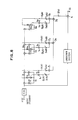
- FIG 8 shows the second embodiment.
- the result g m -(k) is multiplied by the variable coefficient D m (k).
- the Oth-order delayed output v m (k) is also multiplied by the variable coefficient C m (k).
- the two product signals are added in the adder 2 m .
- the adaptive digital filter of the second embodiment functions in the same way as in the first embodiment. Further explanation is therefore omitted here.
- FIG 9 shows a third embodiment comprising M second-order recursive digital filters connected in parallel.
- Each second-order recursive digital filter comprises a scaler R m for multiplying the first-order delayed output g m (k) by a coefficient R m , a first adder 1 m for adding the output of the scaler R m to the Oth-order delayed output signal, a first variable-coefficient scaler C m (k) for multiplying the output v m (k) of the first adder 1 m by a variable coefficient C m (k), a second variable-coefficient scaler D for multiplying the first-order delayed output g m (k) by a variable coefficient D m (k), and a second adder 2 m for adding the output of the first variable-coefficient scaler to the output of the second variable-coefficient scaler.
- An adder 2 m adds the output of the second adder 2 m to the output of the second adder in the previous section 2 m -1 (not
- the input signal applied to the input terminal is fed to all of the second-order recursive digital filters. This input is added to the value of the first-order delayed output g m (k) multiplied by the coefficient a m minus the value of the second-order delayed output multiplied by the coefficient b m .
- the first-order delayed output g m (k) is also multiplied by the coefficient R m and added to the Oth-order delayed output in the adder 1 m .
- the output v m (k) of this adder 1 m is multiplied by the variable coefficient C m .
- the first-order delayed output g m (k) is also multiplied by the variable coefficient D m .
- the two product signals are added in the adder 2 m , and the sum is output to the adder 3 m .
- the adder 3 m adds the output of the adder 2 m to the corresponding output in the preceding section and feeds the result to the corresponding adder 3 m-1 ) in the next section.
- the final output of the filter is obtained from the adder 3 M .
- Figure 10 shows one basic section of the fourth embodiment of the invention.
- the other parts of the embodiment in Figure 10 function in the same way as in the embodiment of Figure 9 and produce the same result. Further explanation is therefore omitted here.
- a fifth embodiment of the invention is shown in Figure 11.
- This embodiment is an echo canceler having an adaptive digital filter similar to the embodiment of Figure 9 but also includes a measure providing for the case in which the R in the denominator polynomial 1 ⁇ RZ .2M in Eq. (15) cannot be ignored.
- the adaptive digital with the transfer function H(z) in this figure is identical to the adaptive digital filter in Figure 6. From Eq. (15) the transfer function H(z) of this adaptive digital filter is:
- a recursive digital filter having a transfer function of 1.1(1 ⁇ Rz ⁇ 2M ) is inserted in series with the unknown system H(z), so:
- the error signal H(z) - N(z) is produced at the output terminal. but this quantity is not in question because it is the estimation error.
Landscapes
- Engineering & Computer Science (AREA)
- Computer Networks & Wireless Communication (AREA)
- Signal Processing (AREA)
- Filters That Use Time-Delay Elements (AREA)
- Cable Transmission Systems, Equalization Of Radio And Reduction Of Echo (AREA)
Applications Claiming Priority (6)
| Application Number | Priority Date | Filing Date | Title |
|---|---|---|---|
| JP544/87 | 1987-01-07 | ||
| JP54287A JPS63169809A (ja) | 1987-01-07 | 1987-01-07 | 適応形デイジタルフイルタシステム |
| JP54487A JPS63169811A (ja) | 1987-01-07 | 1987-01-07 | 適応形デイジタルフイルタ |
| JP542/87 | 1987-01-07 | ||
| JP543/87 | 1987-01-07 | ||
| JP54387A JPS63169810A (ja) | 1987-01-07 | 1987-01-07 | 適応形デイジタルフイルタ |
Publications (3)
| Publication Number | Publication Date |
|---|---|
| EP0274850A2 true EP0274850A2 (fr) | 1988-07-20 |
| EP0274850A3 EP0274850A3 (en) | 1988-08-03 |
| EP0274850B1 EP0274850B1 (fr) | 1992-04-08 |
Family
ID=27274507
Family Applications (1)
| Application Number | Title | Priority Date | Filing Date |
|---|---|---|---|
| EP87310605A Expired EP0274850B1 (fr) | 1987-01-07 | 1987-12-02 | Filtres numériques et annuleurs d'écho adaptatifs |
Country Status (4)
| Country | Link |
|---|---|
| US (1) | US4852036A (fr) |
| EP (1) | EP0274850B1 (fr) |
| CA (1) | CA1318952C (fr) |
| DE (1) | DE3778140D1 (fr) |
Cited By (2)
| Publication number | Priority date | Publication date | Assignee | Title |
|---|---|---|---|---|
| DE19925046A1 (de) * | 1999-06-01 | 2001-05-03 | Alcatel Sa | Verfahren und Vorrichtung zur Unterdrückung von Rauschen und Echos |
| CN1078983C (zh) * | 1995-02-24 | 2002-02-06 | 阿尔卡塔尔意大利公司 | 分步间隔均衡电路及方法 |
Families Citing this family (3)
| Publication number | Priority date | Publication date | Assignee | Title |
|---|---|---|---|---|
| DE4236272A1 (de) * | 1992-10-27 | 1994-04-28 | Siemens Ag | Echokompensationsvorrichtung und 4/2-Drahtschnittstelle mit einer solchen Echokompensationsvorrichtung |
| DE4430189A1 (de) * | 1994-08-25 | 1996-02-29 | Sel Alcatel Ag | Verfahren zur adaptiven Echokompensation |
| JP2947093B2 (ja) * | 1994-11-02 | 1999-09-13 | 日本電気株式会社 | 適応フィルタによるシステム同定の方法および装置 |
-
1987
- 1987-10-30 US US07/114,873 patent/US4852036A/en not_active Expired - Lifetime
- 1987-12-02 DE DE8787310605T patent/DE3778140D1/de not_active Expired - Fee Related
- 1987-12-02 EP EP87310605A patent/EP0274850B1/fr not_active Expired
- 1987-12-15 CA CA000554432A patent/CA1318952C/fr not_active Expired - Lifetime
Cited By (2)
| Publication number | Priority date | Publication date | Assignee | Title |
|---|---|---|---|---|
| CN1078983C (zh) * | 1995-02-24 | 2002-02-06 | 阿尔卡塔尔意大利公司 | 分步间隔均衡电路及方法 |
| DE19925046A1 (de) * | 1999-06-01 | 2001-05-03 | Alcatel Sa | Verfahren und Vorrichtung zur Unterdrückung von Rauschen und Echos |
Also Published As
| Publication number | Publication date |
|---|---|
| CA1318952C (fr) | 1993-06-08 |
| US4852036A (en) | 1989-07-25 |
| EP0274850A3 (en) | 1988-08-03 |
| EP0274850B1 (fr) | 1992-04-08 |
| DE3778140D1 (de) | 1992-05-14 |
Similar Documents
| Publication | Publication Date | Title |
|---|---|---|
| US5014232A (en) | Adaptive digital filter having non-recursive and recursive filter elements | |
| CA2010652C (fr) | Eliminateur d'echos a filtres a reponses impulsionnelles finie et infinie pour eliminer les echos porlonges | |
| US4038536A (en) | Adaptive recursive least mean square error filter | |
| KR0139176B1 (ko) | 다해상도 선형왜곡 보상방법 및 그 장치 | |
| EP0281101B1 (fr) | Circuit d'annulation d'une forme d'onde en entier ou en partie utilisant des filtres non récursifs et récursifs | |
| US6546105B1 (en) | Sound image localization device and sound image localization method | |
| EP0274850B1 (fr) | Filtres numériques et annuleurs d'écho adaptatifs | |
| AU553371B2 (en) | An fir-type balance filter incorporated in the transmitter- receiver unit in a telecommunication system | |
| US5524149A (en) | Circuit arrangement for echo suppression | |
| JPS6243378B2 (fr) | ||
| US4539536A (en) | Parameter-setting approach to obtain high performance CTD transversal filters from devices with significant CTI and FPN | |
| US6968352B1 (en) | Device for digital processing with frequency filtering and reduced computation complexity | |
| US6856684B1 (en) | Device and method for echo compensation in a two-wire full duplex channel transmission method | |
| JP3109389B2 (ja) | 適応フィルタシステム | |
| US4868775A (en) | Adaptive digital filter | |
| JPH10509011A (ja) | 改良されたディジタルフィルタ | |
| JPS59139717A (ja) | 自動等化器 | |
| US5027370A (en) | Circuit arrangement for the equalization of digital signals received in analog form | |
| KR100195220B1 (ko) | 저역통과 iir 필터의 설계방법 및 이에 적합한저역통과iir필터 | |
| JPS63228817A (ja) | 適応デジタルフイルタ | |
| EP0939487A2 (fr) | Filtre d'égalisation/ linéarisation de systèmes non linéaires | |
| JPS63169809A (ja) | 適応形デイジタルフイルタシステム | |
| JPH0691420B2 (ja) | 適応型デイジタルフイルタ | |
| Keerthi et al. | Analysis of the multistage CM array for digital communication signals | |
| JPS6114689B2 (fr) |
Legal Events
| Date | Code | Title | Description |
|---|---|---|---|
| PUAI | Public reference made under article 153(3) epc to a published international application that has entered the european phase |
Free format text: ORIGINAL CODE: 0009012 |
|
| PUAL | Search report despatched |
Free format text: ORIGINAL CODE: 0009013 |
|
| AK | Designated contracting states |
Kind code of ref document: A2 Designated state(s): DE FR GB |
|
| AK | Designated contracting states |
Kind code of ref document: A3 Designated state(s): DE FR GB |
|
| 17P | Request for examination filed |
Effective date: 19880915 |
|
| 17Q | First examination report despatched |
Effective date: 19910118 |
|
| GRAA | (expected) grant |
Free format text: ORIGINAL CODE: 0009210 |
|
| AK | Designated contracting states |
Kind code of ref document: B1 Designated state(s): DE FR GB |
|
| REF | Corresponds to: |
Ref document number: 3778140 Country of ref document: DE Date of ref document: 19920514 |
|
| ET | Fr: translation filed | ||
| PLBE | No opposition filed within time limit |
Free format text: ORIGINAL CODE: 0009261 |
|
| STAA | Information on the status of an ep patent application or granted ep patent |
Free format text: STATUS: NO OPPOSITION FILED WITHIN TIME LIMIT |
|
| 26N | No opposition filed | ||
| PGFP | Annual fee paid to national office [announced via postgrant information from national office to epo] |
Ref country code: GB Payment date: 19931201 Year of fee payment: 7 |
|
| PGFP | Annual fee paid to national office [announced via postgrant information from national office to epo] |
Ref country code: DE Payment date: 19931222 Year of fee payment: 7 |
|
| PGFP | Annual fee paid to national office [announced via postgrant information from national office to epo] |
Ref country code: FR Payment date: 19931230 Year of fee payment: 7 |
|
| PG25 | Lapsed in a contracting state [announced via postgrant information from national office to epo] |
Ref country code: GB Effective date: 19941202 |
|
| GBPC | Gb: european patent ceased through non-payment of renewal fee |
Effective date: 19941202 |
|
| PG25 | Lapsed in a contracting state [announced via postgrant information from national office to epo] |
Ref country code: FR Effective date: 19950831 |
|
| PG25 | Lapsed in a contracting state [announced via postgrant information from national office to epo] |
Ref country code: DE Effective date: 19950901 |
|
| REG | Reference to a national code |
Ref country code: FR Ref legal event code: ST |