EP0274942A2 - Matrixanzeigesystem mit flachem Bildschirm zur geschützten Anzeige von primären Daten für den Betrieb - Google Patents
Matrixanzeigesystem mit flachem Bildschirm zur geschützten Anzeige von primären Daten für den Betrieb Download PDFInfo
- Publication number
- EP0274942A2 EP0274942A2 EP87402822A EP87402822A EP0274942A2 EP 0274942 A2 EP0274942 A2 EP 0274942A2 EP 87402822 A EP87402822 A EP 87402822A EP 87402822 A EP87402822 A EP 87402822A EP 0274942 A2 EP0274942 A2 EP 0274942A2
- Authority
- EP
- European Patent Office
- Prior art keywords
- image
- addressing
- circuits
- odd
- sub
- Prior art date
- Legal status (The legal status is an assumption and is not a legal conclusion. Google has not performed a legal analysis and makes no representation as to the accuracy of the status listed.)
- Granted
Links
Images


Classifications
-
- G—PHYSICS
- G09—EDUCATION; CRYPTOGRAPHY; DISPLAY; ADVERTISING; SEALS
- G09G—ARRANGEMENTS OR CIRCUITS FOR CONTROL OF INDICATING DEVICES USING STATIC MEANS TO PRESENT VARIABLE INFORMATION
- G09G3/00—Control arrangements or circuits, of interest only in connection with visual indicators other than cathode-ray tubes
- G09G3/20—Control arrangements or circuits, of interest only in connection with visual indicators other than cathode-ray tubes for presentation of an assembly of a number of characters, e.g. a page, by composing the assembly by combination of individual elements arranged in a matrix no fixed position being assigned to or needed to be assigned to the individual characters or partial characters
- G09G3/34—Control arrangements or circuits, of interest only in connection with visual indicators other than cathode-ray tubes for presentation of an assembly of a number of characters, e.g. a page, by composing the assembly by combination of individual elements arranged in a matrix no fixed position being assigned to or needed to be assigned to the individual characters or partial characters by control of light from an independent source
- G09G3/36—Control arrangements or circuits, of interest only in connection with visual indicators other than cathode-ray tubes for presentation of an assembly of a number of characters, e.g. a page, by composing the assembly by combination of individual elements arranged in a matrix no fixed position being assigned to or needed to be assigned to the individual characters or partial characters by control of light from an independent source using liquid crystals
- G09G3/3611—Control of matrices with row and column drivers
- G09G3/3648—Control of matrices with row and column drivers using an active matrix
-
- G—PHYSICS
- G09—EDUCATION; CRYPTOGRAPHY; DISPLAY; ADVERTISING; SEALS
- G09G—ARRANGEMENTS OR CIRCUITS FOR CONTROL OF INDICATING DEVICES USING STATIC MEANS TO PRESENT VARIABLE INFORMATION
- G09G3/00—Control arrangements or circuits, of interest only in connection with visual indicators other than cathode-ray tubes
- G09G3/20—Control arrangements or circuits, of interest only in connection with visual indicators other than cathode-ray tubes for presentation of an assembly of a number of characters, e.g. a page, by composing the assembly by combination of individual elements arranged in a matrix no fixed position being assigned to or needed to be assigned to the individual characters or partial characters
- G09G3/34—Control arrangements or circuits, of interest only in connection with visual indicators other than cathode-ray tubes for presentation of an assembly of a number of characters, e.g. a page, by composing the assembly by combination of individual elements arranged in a matrix no fixed position being assigned to or needed to be assigned to the individual characters or partial characters by control of light from an independent source
- G09G3/36—Control arrangements or circuits, of interest only in connection with visual indicators other than cathode-ray tubes for presentation of an assembly of a number of characters, e.g. a page, by composing the assembly by combination of individual elements arranged in a matrix no fixed position being assigned to or needed to be assigned to the individual characters or partial characters by control of light from an independent source using liquid crystals
- G09G3/3611—Control of matrices with row and column drivers
- G09G3/3648—Control of matrices with row and column drivers using an active matrix
- G09G3/3666—Control of matrices with row and column drivers using an active matrix with the matrix divided into sections
-
- G—PHYSICS
- G09—EDUCATION; CRYPTOGRAPHY; DISPLAY; ADVERTISING; SEALS
- G09G—ARRANGEMENTS OR CIRCUITS FOR CONTROL OF INDICATING DEVICES USING STATIC MEANS TO PRESENT VARIABLE INFORMATION
- G09G2310/00—Command of the display device
- G09G2310/02—Addressing, scanning or driving the display screen or processing steps related thereto
- G09G2310/0224—Details of interlacing
-
- G—PHYSICS
- G09—EDUCATION; CRYPTOGRAPHY; DISPLAY; ADVERTISING; SEALS
- G09G—ARRANGEMENTS OR CIRCUITS FOR CONTROL OF INDICATING DEVICES USING STATIC MEANS TO PRESENT VARIABLE INFORMATION
- G09G2330/00—Aspects of power supply; Aspects of display protection and defect management
- G09G2330/08—Fault-tolerant or redundant circuits, or circuits in which repair of defects is prepared
Definitions
- the present invention relates to information display systems by display on a flat screen of the matrix addressing type.
- the invention is particularly applicable in the avionics field for the display of piloting data.
- the display can be of the head-up or head-down type.
- the amount of information to be displayed on the display devices fitted to the dashboard of modern aircraft is becoming more and more important, with conventional electromechanical instrumentation disappearing.
- a certain amount of information to be displayed is essential for flight safety or operation and must therefore be safe and always displayed, or viewable.
- the object of the invention is to satisfy these requirements by implementing a specific structuring of the display system.
- a display system on a flat matrix screen comprising, a display device composed of the flat screen and matrix addressing means controlled to obtain an image resulting from an even image and from an interlaced odd image, these means comprising four groups of circuits for addressing respectively the even lines and columns forming the even image and the odd lines and columns forming the odd image, graphic processor means for developing the video signals to be displayed by addressing columns and scanning signals by addressing lines, the system being characterized in that the graphics processor means are distributed in two subsets, a first subset for developing the even image and a second subset for developing the odd image.
- the resulting advantages translate into enhanced security by a reduced probability of viewing the erroneous information, the proposed structure allowing the detection of such information by observation of the screen.
- the structure used ensures a high level of safety compatible with the strict requirements in terms of airworthiness certification.
- Another advantage results from the continuous availability of essential information, the solution implemented making it possible to protect the display of this data by reproducing it after a failure and thus to keep in operation a display at least restricted to this essential information for the exploitation. This also results in a reduction in maintenance costs by reducing the removal of equipment.
- FIG. 1 we distinguish the structure of the flat screen which is briefly recalled. It essentially consists of a bottom plate 1, made of glass or ceramic, on which are arranged parallel to each other transparent electrodes 2 corresponding to the lines of the screen; a front plate 3 also transparent, made of glass or silica, which forms the front face of the screen and on which is arranged another network of electrodes 4 perpendicular to the first and corresponding to the columns. Between the two thinly spaced plates, and in contact with the two arrays of electrodes forming the matrix, a solid, liquid or gaseous electro-optical material 5, on which the image is formed. For the formation of colors it will be noted that the rows as well as the columns can be distributed successively corresponding to the colors red green and blue so as to produce the desired hues or, by simultaneous control, a monochrome image in black and white.
- the row 2 and column 4 electrodes are connected to integrated control circuits, or addressing circuits (called drivers) which send them electrical signals.
- the points of the screen are addressed line by line, at a rate such that all the points are reached at each image renewal; in general this rate is from 50 to 60 Hz.
- a reaction appears at each addressed point which results in a change in appearance.
- This can take two different forms, either an emission of light, or a change in the power of reflection or transmission of light.
- a lighting device 6 placed at the rear, produces the luminance necessary to ensure the visualization of the data displayed on the screen.
- the materials corresponding to the first case are based on active devices such as plasma screens, screens luminescent or light-emitting diodes, VFD (Vacum Fluorescent Display) screens, etc ...
- the materials corresponding to the second case are based on passive devices.
- the best known are constituted by liquid crystals which can be of several types: cholesteric, nematic, smectic, ferroelectric, etc ...
- a first family groups together the active devices in which each picture element is placed in series with a nonlinear element of the varistor (VRD) type, thin film transistors (TFT), head-to-tail diodes.
- the second family uses materials with an electro-optical effect with memory; mention may be made of smectic liquid crystals A operating in a mixed thermal and electrical mode and smectic ferroelectric liquid crystals.
- the invention applies more particularly and advantageously to realizations of flat screen with liquid crystals and with a nematic electro-optical effect in a helix which, associated with an active matrix with TFT and with filters colored, make it possible to produce high resolution color matrix flat screens capable, in particular, of viewing all the piloting information of a modern aircraft.
- High resolution liquid crystal display screens have two groups of circuits for addressing even rows and columns relating to the development of a so-called even image and two other groups for addressing rows and odd columns relating to the development of a so-called odd image.
- This operating principle resembles that of television where the image is formed by two interlaced half-frames. But, unlike television where the two half-frames are drawn successively in time, the even and odd images are drawn simultaneously, all the points of the image being reached at each image renewal.
- These four groups are visible in FIG. 1, the connections to the electrodes of the two groups are shown relative to an even image; the connections of the other two groups have not been shown to simplify the representation. To obtain a high resolution image these four groups present an additional partition of the circuits.
- each column addressing group is divided into three circuits 7A, 7B, 7C for the even columns, 9A, 9B, 9C for the odd columns and each row addressing group is divided into two blocks 10A and 10B for even lines, 12A and 12B for odd lines.
- the partition values 2 and 3 considered have been taken as a non-limiting example.
- An additional graphics processor assembly produces the video signals SV1, SV2, SV3, which are applied respectively to the different addressing circuits columns 7 and 9, and a clock signal H which increments the line counters located in the line addressing circuits 10 and 12.
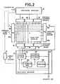
- this additional graphics processor assembly consists of a first graphics processor 21 which produces the signals intended for circuits 7 and 10 which make it possible to form the even image, and a second graphics processor 22 which produces the signals for the circuits 9 and 12 used to obtain the odd image.
- Each of these processors comprises, as indicated for block 21, at least one symbol generator circuit 211 associated with an image memory 212.
- the control signals and those corresponding to the information to be displayed reach the processors 21 and 22 through interface circuits, respectively 23 and 24.
- Circuits indicated by circles can for example be sensors whose signals are to be translated by a determined symbology. It can be considered, for example, that the circuit C2A concerns an altitude detector whose signal is after processing applied via the interface 24 to the processor 22.
- Another device for measuring altitude C2B distinct from the previous one is used to provide the same information through the interface 23 to the processor 21.
- This redundancy with different multiple sources to translate the same information to be viewed is frequent on airborne or other equipment, for security reasons; it is used in the proposed system when it is classified information which is essential for operation and whose display must be preserved.
- Each graphics processor comprises, in addition to the symbol generator and the image memory, the essential elements indicated in FIG. 2, namely a video controller circuit 213 which manages the accesses of the symbol generator to the image memory and supplies the signals. scanning the screen for reading in television mode; the circuit 214 represents a management and calculation circuit such as a microprocessor assembly which receives by a bus and the interface 23 not shown the information to be displayed on the screen.
- the layout of the two even and odd images having to be done simultaneously the subsets 21 and 22 are coordinated from the synchronization point of view; one of the video controller circuits, for example 213, is declared master and supplies the synchronization signals to the other video controller which is declared slave.
- the synchronization signals are: a clock signal at the point rate and the line and image synchronization signals.
- FIG. 2 represents the simplest organization envisaged which uses the two graphics processors 21 and 22 and which allows, in the event of a channel failure, the maintenance of display of the image with a resolution half by the another way. Information can therefore always be available and usable.
- This solution also has a certain flexibility the two channels corresponding to the even image and the odd image can be made asymmetrical, the information coming as it was said from different data sources, the difference can also be made at the level of the symbol generator, the generator 211 at 21 being different from that used at 22.
- the two interlaced images become different which visually alerts the operator who can no longer do trust the information displayed. This involves on the part of the operator, the pilot on board an aircraft, a verification and control procedure on other instruments available for the same information so as to eliminate, if necessary, the faulty lane and to reconfigure its visualization on the remaining channel.
- the reconfiguration will cause, if necessary, a change in the master-slave allocation of the remaining video controller.
- This reconfiguration can be done simply by a mechanical switch device actuated by the operator. It can also be envisaged to program the control of this switch to automatically respond to the different cases.
- processors specialized in signal processing called DSP (abbreviation of Digital Signal Processor). These graphics processors make it possible to calculate the plot of the symbologies to be stored in the image memories.
- DSP abbreviation of Digital Signal Processor
- each processor instead of having a single symbol generator comprises several which work in parallel, each of them being associated to his image memory.
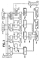
- the processor 214 is detailed by these main elements a microprocessor 214A, a program memory 214B and a data memory 214C. The program and data buses are shown.
- the chain A is master and imposes on the other slave chains B, C, D the synchronizations of the write and read modes (pixel, line and frame synchronization).
- the video signals delivered by the image memories are applied to a video multiplexer 215, then through an output interface circuit 216 are sent, as well as the clock signal, to the even column addressing circuits and to the circuits of addressing even lines as shown in the previous figures.
- the complementary circuits shown are produced according to known techniques and include smoothing circuits 217A, 217B, 217C, a surfacing circuit 218, a color palette circuit 219A and a pixel storage circuit 219B.
- smoothing circuits 217A, 217B, 217C a surfacing circuit 218, a color palette circuit 219A and a pixel storage circuit 219B.
- the master chain A produces the symbology relating to the static image
- the chain B the symbology relating to the dynamic image
- the chain C the surface symbology
- the chain D relates to symbols from a weather radar.
- the 217C smoothing circuit is not compulsory.
- the smoothing circuit 217A, B or C gives the displayed trace an analog appearance. It especially removes the steps of stairs which are due to the discretization of the image memory and of the screen 5.
- the smoothing is obtained by weighting the level of the video signal of the points of the image through which the trace passes as well as that of the adjacent points.
- the smoothing circuit can, for example, consist of a set of read-only memories which, depending on the position and the direction of the trace, provide the coefficients to be applied to the points of the trace.
- the surfacing circuit 218 allows the interior of surfaces to be filled with a certain color.
- the color codes of the points of each surface are stored in the image memory.
- the color palette circuit 219A makes it possible to code the levels of the video R, G, B from the color codes provided by the image memory. Transcoding is obtained by a table which can be loaded dynamically by the processor. This allows to have an infinity of colors.
- the pixel arrangement circuit 219A from the knowledge of the distribution of the color points of the screen (stored in read-only memory for example) ensures the selection of the right video to the screen 5.
- FIG. 4 represents a third embodiment according to which the display screen 5 is divided into several bands, for example into three vertical bands 5A, 5B, 5C.
- Each band is controlled through the associated column addressing circuits 9A, 9B, 9C, 11A, 11B, 11C by a pair of graphics processors 21A and 22A for the first band 5A, 21B and 22B for the second band 5B and 21C and 22C for the third band 5C.
- Each processor comprises as symbolized in block 21B a generator of symbols and an associated image memory.
- the two graphics processors associated with a strip trace all the information to be displayed in this strip.
- the synchronization switch circuit 29A is derived from that 29 of FIG. 2; it brings together the various switches useful for performing the necessary reconfigurations in the event of channel failures, each channel corresponding to a strip of the screen and to the associated graphics processors.
- the advantages of this third embodiment are that, in the event of a channel failure, either at the level of the symbol generator, column addressing circuits or even of the screen, or even upstream of the processor, the processing and the visualization of the essential information lost can be taken into account by another channel or by several of the other channels. We can thus present with the remaining elements a complete image with a reduced format usable by the pilot.
- FIG. 5 illustrates the case where the channel corresponding to the band 5A breaks down.
- the programming is such that the symbology which existed in this surface band A A1 C C1 is transferred to the level of the assembly remaining delimited by the surface A1 B C1 D of the screen with compression in the direction of the lines.
- Programming can also be provided to maintain homothety to the new figure by also reducing the height of the image; under these conditions, the complete image occurs in the area A2 B2 C2 D2 indicated with a reduction of a third compared to the case where the entire screen is viewed.
Landscapes
- Engineering & Computer Science (AREA)
- Chemical & Material Sciences (AREA)
- Crystallography & Structural Chemistry (AREA)
- Physics & Mathematics (AREA)
- Computer Hardware Design (AREA)
- General Physics & Mathematics (AREA)
- Theoretical Computer Science (AREA)
- Controls And Circuits For Display Device (AREA)
- Control Of Indicators Other Than Cathode Ray Tubes (AREA)
- Devices For Indicating Variable Information By Combining Individual Elements (AREA)
Applications Claiming Priority (2)
| Application Number | Priority Date | Filing Date | Title |
|---|---|---|---|
| FR8617575A FR2608300B1 (fr) | 1986-12-16 | 1986-12-16 | Systeme de visualisation sur ecran plat matriciel avec affichage protege des donnees primordiales pour l'exploitation |
| FR8617575 | 1986-12-16 |
Publications (3)
| Publication Number | Publication Date |
|---|---|
| EP0274942A2 true EP0274942A2 (de) | 1988-07-20 |
| EP0274942A3 EP0274942A3 (en) | 1988-07-27 |
| EP0274942B1 EP0274942B1 (de) | 1992-03-18 |
Family
ID=9341942
Family Applications (1)
| Application Number | Title | Priority Date | Filing Date |
|---|---|---|---|
| EP87402822A Expired - Lifetime EP0274942B1 (de) | 1986-12-16 | 1987-12-11 | Matrixanzeigesystem mit flachem Bildschirm zur geschützten Anzeige von primären Daten für den Betrieb |
Country Status (5)
| Country | Link |
|---|---|
| US (1) | US4859997A (de) |
| EP (1) | EP0274942B1 (de) |
| JP (1) | JPS63163396A (de) |
| DE (1) | DE3777606D1 (de) |
| FR (1) | FR2608300B1 (de) |
Cited By (6)
| Publication number | Priority date | Publication date | Assignee | Title |
|---|---|---|---|---|
| EP0368572A3 (de) * | 1988-11-05 | 1991-08-14 | SHARP Corporation | Steuereinrichtung und -verfahren für eine Flüssigkristallanzeigetafel |
| FR2660471A1 (fr) * | 1990-03-30 | 1991-10-04 | Sextant Avionique | Dispositif de visualisation de securite utilisant un ecran a matrice de points et tableau de bord d'aeronef comportant au moins un tel dispositif. |
| EP0402850A3 (de) * | 1989-06-12 | 1991-10-23 | Kabushiki Kaisha Toshiba | Bildpunktmatrixanzeigegerät |
| EP0506530A1 (de) * | 1991-03-29 | 1992-09-30 | Thomson-Lcd | Matrixanzeige mit verbesserter Auflösung und Adressierungsverfahren einer solchen Anzeige |
| EP0673012A3 (de) * | 1994-03-11 | 1996-01-10 | Canon Information Syst Res | Steuerung für eine Anzeige mit mehrfachen gemeinsamen Zeilen für jeden Pixel. |
| US6002385A (en) * | 1994-03-11 | 1999-12-14 | Canon Kabushiki Kaisha | Computer display system controller |
Families Citing this family (26)
| Publication number | Priority date | Publication date | Assignee | Title |
|---|---|---|---|---|
| JPH02157813A (ja) * | 1988-12-12 | 1990-06-18 | Sharp Corp | 液晶表示パネル |
| US5206749A (en) * | 1990-12-31 | 1993-04-27 | Kopin Corporation | Liquid crystal display having essentially single crystal transistors pixels and driving circuits |
| US5258320A (en) * | 1990-12-31 | 1993-11-02 | Kopin Corporation | Single crystal silicon arrayed devices for display panels |
| US5743614A (en) * | 1990-12-31 | 1998-04-28 | Kopin Corporation | Housing assembly for a matrix display |
| US5528397A (en) * | 1991-12-03 | 1996-06-18 | Kopin Corporation | Single crystal silicon transistors for display panels |
| US6320568B1 (en) | 1990-12-31 | 2001-11-20 | Kopin Corporation | Control system for display panels |
| US5376979A (en) * | 1990-12-31 | 1994-12-27 | Kopin Corporation | Slide projector mountable light valve display |
| US5321505A (en) * | 1991-01-11 | 1994-06-14 | Microelectronics & Computer Technology Corporation | Computer scalable visualization system |
| AU5362694A (en) * | 1992-11-06 | 1994-06-08 | Virtual Vision, Inc. | Head mounted video display system with portable video interface unit |
| JP3454971B2 (ja) * | 1995-04-27 | 2003-10-06 | 株式会社半導体エネルギー研究所 | 画像表示装置 |
| US6025821A (en) * | 1998-02-10 | 2000-02-15 | Prince Corporation | Drive system for vacuum fluorescent display and method therefor |
| US6140993A (en) * | 1998-06-16 | 2000-10-31 | Atmel Corporation | Circuit for transferring high voltage video signal without signal loss |
| EP1783599A3 (de) * | 1998-09-04 | 2007-06-13 | Innovative Solutions & Support, Inc. | Flachbildschirm mit zwei CPU's für Flugzeugcockpit |
| AU5808299A (en) * | 1998-09-04 | 2000-03-27 | Innovative Solutions And Support Inc. | Flat panel display using dual cpu's for an aircraft cockpit |
| GB9902343D0 (en) * | 1999-02-04 | 1999-03-24 | Sharp Kk | overnment Of The United Kingdom Of Great Britain And Northern Ireland The Addressable matrix arrays |
| US6671406B1 (en) * | 1999-12-29 | 2003-12-30 | Honeywell International Inc. | System, method and apparatus for pattern recognition with application to symbol recognition and regeneration for a caligraphic display |
| JP3873139B2 (ja) * | 2000-06-09 | 2007-01-24 | 株式会社日立製作所 | 表示装置 |
| US20020112479A1 (en) * | 2001-01-09 | 2002-08-22 | Keefer Bowie G. | Power plant with energy recovery from fuel storage |
| FR2843646B1 (fr) * | 2002-08-13 | 2004-10-29 | Thales Sa | Dispositif de visualisation a architecture electronique securisee |
| FR2843823B1 (fr) * | 2002-08-20 | 2006-04-21 | Thales Sa | Visualisations a cristaux liquides a commande fiabilisee |
| WO2005035469A1 (en) * | 2003-10-02 | 2005-04-21 | Shell Internationale Research Maatschappij B.V. | Production of 1-alkenes from mixed olefin streams using catalytic distillation |
| GB2500401B (en) | 2012-03-20 | 2020-06-03 | Ge Aviat Systems Ltd | Apparatus for an aircraft cockpit display |
| GB2501255B (en) | 2012-04-16 | 2018-04-11 | Ge Aviat Systems Ltd | Apparatus for aircraft dual channel display |
| GB2507524B (en) * | 2012-11-01 | 2016-02-24 | Ge Aviat Systems Ltd | Apparatus for aircraft dual channel display |
| WO2019149348A1 (en) * | 2018-01-31 | 2019-08-08 | Koncar - Inzenjering Za Energetiku I Transport D.D. | Method and device for displaying safety unit signals with information regarding reliability of displayed signals |
| CN115691369B (zh) | 2021-07-21 | 2025-02-21 | 北京京东方光电科技有限公司 | 显示面板的显示方法及其显示控制装置、显示装置 |
Family Cites Families (3)
| Publication number | Priority date | Publication date | Assignee | Title |
|---|---|---|---|---|
| US4468659A (en) * | 1980-08-25 | 1984-08-28 | Sharp Kabushiki Kaisha | Electroluminescent display panel assembly |
| JPS6180226A (ja) * | 1984-09-28 | 1986-04-23 | Toshiba Corp | アクテイブ・マトリツクス駆動装置 |
| FR2571571B1 (fr) * | 1984-10-05 | 1986-11-28 | Thomson Csf | Procede d'elaboration d'images video synthetiques en vue d'une visualisation en temps reel et a haute densite d'information et dispositif utilisant ce procede |
-
1986
- 1986-12-16 FR FR8617575A patent/FR2608300B1/fr not_active Expired
-
1987
- 1987-12-11 DE DE8787402822T patent/DE3777606D1/de not_active Expired - Fee Related
- 1987-12-11 EP EP87402822A patent/EP0274942B1/de not_active Expired - Lifetime
- 1987-12-14 US US07/132,563 patent/US4859997A/en not_active Expired - Fee Related
- 1987-12-15 JP JP62317250A patent/JPS63163396A/ja active Pending
Cited By (8)
| Publication number | Priority date | Publication date | Assignee | Title |
|---|---|---|---|---|
| EP0368572A3 (de) * | 1988-11-05 | 1991-08-14 | SHARP Corporation | Steuereinrichtung und -verfahren für eine Flüssigkristallanzeigetafel |
| EP0402850A3 (de) * | 1989-06-12 | 1991-10-23 | Kabushiki Kaisha Toshiba | Bildpunktmatrixanzeigegerät |
| US5241304A (en) * | 1989-06-12 | 1993-08-31 | Kabushiki Kaisha Toshiba | Dot-matrix display apparatus |
| FR2660471A1 (fr) * | 1990-03-30 | 1991-10-04 | Sextant Avionique | Dispositif de visualisation de securite utilisant un ecran a matrice de points et tableau de bord d'aeronef comportant au moins un tel dispositif. |
| EP0506530A1 (de) * | 1991-03-29 | 1992-09-30 | Thomson-Lcd | Matrixanzeige mit verbesserter Auflösung und Adressierungsverfahren einer solchen Anzeige |
| FR2674663A1 (fr) * | 1991-03-29 | 1992-10-02 | Thomson Lcd | Ecran matriciel a definition amelioree et procede d'adressage d'un tel ecran. |
| EP0673012A3 (de) * | 1994-03-11 | 1996-01-10 | Canon Information Syst Res | Steuerung für eine Anzeige mit mehrfachen gemeinsamen Zeilen für jeden Pixel. |
| US6002385A (en) * | 1994-03-11 | 1999-12-14 | Canon Kabushiki Kaisha | Computer display system controller |
Also Published As
| Publication number | Publication date |
|---|---|
| US4859997A (en) | 1989-08-22 |
| FR2608300B1 (fr) | 1989-03-31 |
| FR2608300A1 (fr) | 1988-06-17 |
| EP0274942B1 (de) | 1992-03-18 |
| JPS63163396A (ja) | 1988-07-06 |
| DE3777606D1 (de) | 1992-04-23 |
| EP0274942A3 (en) | 1988-07-27 |
Similar Documents
| Publication | Publication Date | Title |
|---|---|---|
| EP0274942B1 (de) | Matrixanzeigesystem mit flachem Bildschirm zur geschützten Anzeige von primären Daten für den Betrieb | |
| US8891032B2 (en) | Multi-view display | |
| EP0625861B1 (de) | Räumlicher Lichtmodulator und richtungsabhängiger Anzeigesystem | |
| EP1887807A1 (de) | Hochauflösende umschaltbare 2D/3D-Anzeigevorrichtung | |
| CN101551984B (zh) | 一种时分多视显示装置及一种时分多视显示方法 | |
| EP2174315B1 (de) | Integriertes verfahren zur erkennung eines bilddefekts in einem flüssigkristallbildschirm | |
| CN101432789A (zh) | 显示器、仪表盘、光学系统和光学仪器 | |
| RU2005129545A (ru) | Способ и система для создания пространственных изображений | |
| EP0976122B1 (de) | Matrixanzeigeadressierungsverfahren | |
| FR2989503A1 (fr) | Dispositif pour afficheur dans l'habitacle d'un aeronef | |
| KR100362957B1 (ko) | 디스플레이장치및디스플레이시스템 | |
| WO2004017294A1 (fr) | Dispositif de visualisation a architecture electronique securisee | |
| US20100007723A1 (en) | Image display device, image display method, and image display program | |
| FR2499276A1 (fr) | Dispositif d'affichage matriciel a plusieurs jeux d'electrodes et son procede de commande | |
| WO2020084338A1 (fr) | Dispositif d'affichage permettant un affichage jour et nuit | |
| CN101739912A (zh) | 显示器 | |
| EP0086677B1 (de) | Echtzeiterfassungs- und Rückerstattungseinrichtung für rasterabgetastetes Bild | |
| WO2005096261A1 (fr) | Dispositif de detection d'image figee sur un ecran a cristaux liquides | |
| EP0178219A1 (de) | Verfahren zur Verarbeitung von synthetischen Videobildern für Anzeige in Echtzeit und mit hoher Informationsdichte und dieses Verfahren verwendende Anordnung | |
| US4812019A (en) | Method for producing the first differential of a two-dimensional image and optical structural element for performing the method | |
| FR2666165A1 (fr) | Procede de presentation d'images sur un ecran matriciel et systeme pour la mise en óoeuvre du procede. | |
| FR2660471A1 (fr) | Dispositif de visualisation de securite utilisant un ecran a matrice de points et tableau de bord d'aeronef comportant au moins un tel dispositif. | |
| FR2644001A1 (fr) | Systeme de visualisation d'images | |
| FR2584521A1 (fr) | Dispositif d'affichage electro-optique a cristal liquide | |
| FR2843823A1 (fr) | Visualisations a cristaux liquides a commande fiabilisee |
Legal Events
| Date | Code | Title | Description |
|---|---|---|---|
| PUAI | Public reference made under article 153(3) epc to a published international application that has entered the european phase |
Free format text: ORIGINAL CODE: 0009012 |
|
| PUAL | Search report despatched |
Free format text: ORIGINAL CODE: 0009013 |
|
| AK | Designated contracting states |
Kind code of ref document: A2 Designated state(s): DE GB IT |
|
| AK | Designated contracting states |
Kind code of ref document: A3 Designated state(s): DE GB IT |
|
| 17P | Request for examination filed |
Effective date: 19881222 |
|
| RAP3 | Party data changed (applicant data changed or rights of an application transferred) |
Owner name: THOMSON-CSF |
|
| 17Q | First examination report despatched |
Effective date: 19910219 |
|
| GRAA | (expected) grant |
Free format text: ORIGINAL CODE: 0009210 |
|
| AK | Designated contracting states |
Kind code of ref document: B1 Designated state(s): DE GB IT |
|
| ITF | It: translation for a ep patent filed | ||
| REF | Corresponds to: |
Ref document number: 3777606 Country of ref document: DE Date of ref document: 19920423 |
|
| GBT | Gb: translation of ep patent filed (gb section 77(6)(a)/1977) | ||
| PLBE | No opposition filed within time limit |
Free format text: ORIGINAL CODE: 0009261 |
|
| STAA | Information on the status of an ep patent application or granted ep patent |
Free format text: STATUS: NO OPPOSITION FILED WITHIN TIME LIMIT |
|
| 26N | No opposition filed | ||
| PGFP | Annual fee paid to national office [announced via postgrant information from national office to epo] |
Ref country code: GB Payment date: 19981118 Year of fee payment: 12 |
|
| PG25 | Lapsed in a contracting state [announced via postgrant information from national office to epo] |
Ref country code: GB Free format text: LAPSE BECAUSE OF NON-PAYMENT OF DUE FEES Effective date: 19991211 |
|
| GBPC | Gb: european patent ceased through non-payment of renewal fee |
Effective date: 19991211 |
|
| PGFP | Annual fee paid to national office [announced via postgrant information from national office to epo] |
Ref country code: DE Payment date: 20051209 Year of fee payment: 19 |
|
| PG25 | Lapsed in a contracting state [announced via postgrant information from national office to epo] |
Ref country code: IT Free format text: LAPSE BECAUSE OF NON-PAYMENT OF DUE FEES;WARNING: LAPSES OF ITALIAN PATENTS WITH EFFECTIVE DATE BEFORE 2007 MAY HAVE OCCURRED AT ANY TIME BEFORE 2007. THE CORRECT EFFECTIVE DATE MAY BE DIFFERENT FROM THE ONE RECORDED. Effective date: 20051211 |
|
| PG25 | Lapsed in a contracting state [announced via postgrant information from national office to epo] |
Ref country code: DE Free format text: LAPSE BECAUSE OF NON-PAYMENT OF DUE FEES Effective date: 20070703 |