EP0275212A2 - NAND-Stapelfestwertspeicher - Google Patents
NAND-Stapelfestwertspeicher Download PDFInfo
- Publication number
- EP0275212A2 EP0275212A2 EP88300339A EP88300339A EP0275212A2 EP 0275212 A2 EP0275212 A2 EP 0275212A2 EP 88300339 A EP88300339 A EP 88300339A EP 88300339 A EP88300339 A EP 88300339A EP 0275212 A2 EP0275212 A2 EP 0275212A2
- Authority
- EP
- European Patent Office
- Prior art keywords
- array
- node
- columns
- column
- stacks
- Prior art date
- Legal status (The legal status is an assumption and is not a legal conclusion. Google has not performed a legal analysis and makes no representation as to the accuracy of the status listed.)
- Granted
Links
Images


Classifications
-
- G—PHYSICS
- G11—INFORMATION STORAGE
- G11C—STATIC STORES
- G11C17/00—Read-only memories programmable only once; Semi-permanent stores, e.g. manually-replaceable information cards
- G11C17/08—Read-only memories programmable only once; Semi-permanent stores, e.g. manually-replaceable information cards using semiconductor devices, e.g. bipolar elements
- G11C17/10—Read-only memories programmable only once; Semi-permanent stores, e.g. manually-replaceable information cards using semiconductor devices, e.g. bipolar elements in which contents are determined during manufacturing by a predetermined arrangement of coupling elements, e.g. mask-programmable ROM
- G11C17/12—Read-only memories programmable only once; Semi-permanent stores, e.g. manually-replaceable information cards using semiconductor devices, e.g. bipolar elements in which contents are determined during manufacturing by a predetermined arrangement of coupling elements, e.g. mask-programmable ROM using field-effect devices
- G11C17/123—Read-only memories programmable only once; Semi-permanent stores, e.g. manually-replaceable information cards using semiconductor devices, e.g. bipolar elements in which contents are determined during manufacturing by a predetermined arrangement of coupling elements, e.g. mask-programmable ROM using field-effect devices comprising cells having several storage transistors connected in series
Definitions
- the present invention relates to electronic memories and, more particulary, to a NAND stack Read Only Memory (ROM).
- ROM Read Only Memory
- a memory design embodying the present invention which utilizes a dense array packing technique and lends itself to easy decoding.
- the design takes advantage of the increased packing density of the conventional NAND ROM configuration (over the more traditional NOR ROM configuration) and, at the same time, eliminates most of the multiplexing present in the conventional NAND ROM design. Accordingly, array size and capacitance are significantly reduced, leading to smaller chip dimensions and faster access times. Specifically column capacitance and hence column charge-up time are reduced.
- NAND stack ROM arrays consist of columns of series connected semiconductor switching devices. The devices are fabricated as either enhancement mode or depletion mode devices to reflect programmed data. In the conventional NAND stack ROM configuration, the stacks are configured in pairs, called "pages". Each page consists of two spaced parallel stacks of series connected bit transistors. Each page has a "one of two" multiplexer formed from four page decode transistors. Two page decode transistors are located at the end of each stack, a depletion mode transistor, and an enhancement mode transistor. To read data, the proper page decode line is brought high, accessing a particular page. Simultaneously, one of the bit decode lines is brought low and the input to the sense amplifier, which is selected by a multiplexer at the top of the array, either rises or falls.
- Each stack in the ROM now proposed has one less decode transistor in it than the stack of a conventional NAND stack ROM with the same number of bits.
- a 256K array with 8-bit high stacks in a configuration according to the present invention has over 32,000 fewer transistors than a comparable array in the conventional arrangement.
- the implementation of the present invention has no need for horizontal ground straps of diffusion, required in the conventional layout. Column selection is achieved utilizing "virtual ground" lines running vertically in the array.
- ROMs designed in accordance with the present invention have columns which are 40% less capacitive as calculated using the same design rules and process parameters. This translates into a 12%-20% decrease in column charge-up time, depending upon the operating voltage of the ROM column.
- Adjacent columns in the ROM array of the invention described below are tied to alternating sense amplifiers in the same way as X-matrix ROM columns are organized. Interference between a column being selected and adjacent columns, as well as sneak paths, which are current problems in X-matrix NOR ROM designs, are significantly reduced.
- the multiplexer interposed between the stacks and the sense amplifier are actuated by the same virtual ground lines, which run vertically in the array. These lines do not increase the array's width since the lines' horizontal axis is diffusion limited in the process technology used to develop the described embodiment of the invention.
- the multiplexer is gated by lines running horizontally along the top of the array using extra chip area. Because of these dual purpose virtual ground lines now proposed, a column may have only one multiplexer transistor to pass before the input of its sense amplifier, yet a 256K chip may have as few as one sense amplifier per output, without increasing chip length.
- CMOS complementary metal-oxide-semiconductor
- NMOS complementary metal-oxide-semiconductor
- This new design will reduce power consumption in those NMOS ROMs which limit multiplexing at the top of the array by using more than one sense amplifier per output.
- the virtual ground NAND stack ROM design substantially reduces array size and column capacitance, hence, decreasing total chip area and column charge-up time. It also combines the advantages of single transistor multiplexing at the top of the array with the low power consumption associated with limiting the number of sense amplifiers, without increasing the area of the circuitry peripheral to the array. The implementation of the present invention is also expected to significantly improve wafer yields.
- the preferred implementation of the invention described below is intended to meet the following objectives having regard to conventional practice:- to provide a NAND stack ROM which utilizes a dense array packing technique; to provide a NAND stack ROM which lends itself to easy decoding; to provide a NAND stack ROM with faster access times; to provide a NAND stack ROM wherein column selection is accomplished utilizing virtual ground lines running vertically through the array, thereby eliminating the necessity for horizontal ground straps of diffusion; to provide a NAND stack ROM with significantly reduced column capacitance; to provide a NAND stack ROM with a simplified multiplexer; to provide a NAND stack ROM which reduces the number of sense amplifiers required; to provide a design technique for fabricating a NAND stack ROM which can be implemented in CMOS or NMOS; to provide a NAND stack ROM with significantly improved wafer yields.
- a NAND stack ROM array is formed in a semiconductor substrate.
- substrate includes a well or other suitable structure.
- the array comprises bit select means and a plurality of bit switching means, each having input means and an output circuit. Each of the input means is operably connected to the bit select means.
- the output circuits are operably connected in series between first and second nodes to form a stack. Substantially colinearly aligned stacks form a column.
- Means are provided for applying a virtual ground signal to the first node.
- the signal applying means comprises a conductive region extending through the substrate in the direction of the column.
- Means are provided for sensing the state of the second node.
- means are provided for precharging the second node. The precharging means make it possible to optimize the speed of the array.
- a single stack select switching means is associated with each stack. It has an output circuit operably interposed between the series connected output circuits of the bit switching means and the second node.
- the stack select switching means preferably comprises an enhancement mode transistor only.
- multiplex means are operably interposed between the sensing means and the second node. The multiplex means is operably connected to the conductive region.
- the second node may comprise first and second electrically connected sections located at either end of the column.
- the first node is located between the stacks.
- a NAND stack ROM array formed on a semiconductor substrate including bit select means and bit switching means.
- Each of the bit switching means has an input means and an output circuit. Rows of input means are operably connected to the bit select means.
- the output circuits are operably connected in series between first and second nodes to form stacks. Substantially colinearly aligned stacks form columns.
- Column select means are provided.
- the column select means includes a plurality of outputs and means for applying a virtual ground signal to a selected one of the outputs.
- Conductive regions operably connect each of the outputs to the first node in a different one of the columns. The conductive regions extend through the substrate generally in the direction of the columns. Means are provided for sensing the state of the second node of the column whose first node is connected to the selected output.
- means are provided for precharging the second node of each of the columns. This permits the speed of the array to be optimized.
- the array further comprises stack select means.
- the stack select means include a single switching means associated with each of the stacks and having an output circuit operably interposed between the bit switching means and the second node.
- the single switching means preferably comprises an enhancement node transistor only.
- multiplex means are operably interposed between the sensing means and the second node of each of the stacks.
- the multiplex means are operably connected to the conductive regions.
- the sensing means comprises a pair of sense amplifiers.
- the multiplex means operably connects adjacent stacks to different sense amplifiers in the pair.
- a NAND stack ROM array formed on a semiconductor substrate includes bit select means and sets of first and second substantially colinearly aligned stacks of bit switching means.
- Each bit switching means has an input means and an output circuit.
- the input means of the stacks in each set are operably connected in rows to the bit select means.
- the output circuits of the bit switching means of the stacks in each set are operably connected in series.
- the stacks in each of the sets extend between an intermediate node and first and second end nodes, respectively.
- the sets form substantially parallel columns.
- Column select means are provided.
- the column select means include a plurality of outputs and means for applying a virtual ground signal to a selected one of the outputs. Conductive regions operably connect each of the outputs with a different one of the intermediate nodes and extend through the substrate substantially in a direction of the columns. Means are provided for sensing the state of the end node of the column connected to the selected one of the outputs.
- means are provided for precharging the end nodes of each of the columns. This permits the speed of the array to be optimized.
- a conventional NAND stack ROM includes a substrate or well in which the array is formed.
- the array includes a plurality of pages, generally designated P, consisting of adjacent stacks S.
- Each stack S consists of, for example, eight N-channel bit transistors.
- Colinear stacks S form columns.
- Each stack S is operably connected between an intermediate node 10 connected to ground by a horizontal diffusion strip 11 and a pair of page decode transistors 12, 14 and 12 ⁇ , 14 ⁇ , respectively, one of which is an enhancement mode transistor, and the other of which is a depletion mode transistor.
- Each pair of page decode transistors 12, 14 and 12 ⁇ , 14 ⁇ are interposed between the stack and an end node 16, 16 ⁇ . End nodes 16 and 16 ⁇ are electrically interconnected by vertical metal lines 13.
- Node 16 is connected through an N-channel decoder transistor 18 to a sense amplifier 20.
- Node 16 ⁇ is connected to the output of a column select circuit.
- the column select circuit preferably serves to precharge the nodes 16, 16 ⁇ of a selected column. This optimizes the speed of the ROM.
- each page includes two stacks consisting of, for example, 8 bit transistors each and a "one of two" multiplexer comprised of the four page decode transistors 12, 14 and 12 ⁇ , 14 ⁇ .
- the column select circuit precharges a selected column by applying a voltage to the node 16, 16 ⁇ associated therewith.
- the selected page decode line is then brought high, accessing either the right or left stack of a particular page.
- one of the bit decode lines is brought low and the input to the sense amplifier 20, which is selected by the multiplexer 18 at the top of the array, either rises or falls, depending upon whether the selected stack has become conductive, thereby connecting node 16 or 16 ⁇ with grounded node 10. If the stack has been conductive, then the charge on the node 16, 16 ⁇ will dissipate to ground. Otherwise, node 16, 16 ⁇ will charge. This is sensed by sense amplifier 20 through transistor 18.
- each column includes colinear stacks S of (for example) eight N-channel bit transistors with an intermediate node 30 and end nodes 32, 32 ⁇ .
- a single enhancement node stack decode transistor 34, 34 ⁇ is interposed between the stack and node 32, 32 ⁇ .
- nodes 32 ⁇ are connected to a voltage source V DD through a P-channel transistor 36, the input terminal of which is conditionally connected to a voltage reference source V REF . This permits the ROM to operate at maximum speed.
- Node 32 of each column is connected through a pair of parallel P-channel transistors 38 to a sense amplifier.
- Nodes 30 are connected to conductive metal lines 40 which run vertically through the substrate.
- lines 40 are parallel to, but spaced from, the columns.
- Each of the lines 40 extends from the output of a column decoder 42 which applies a "virtual ground” signal of approximately 0 volts to the line when it is selected (otherwise, applies a "high").
- Line 40 is connected to nodes 30 of adjacent columns and also to the inputs of P-channel decoder transistors 38.
- a particular row of stacks is accessed by bringing the stack decode line high such that the stack decode transistor 34, 34 ⁇ of the selected stack S is turned on.
- a column is selected by bringing a virtual ground line 40 associated therewith to a low state. To read the data, one of the bit lines is brought low at the same time as the stack is accessed and the column is selected.
- the ROM of Fig. 2 has one less (depletion mode page decode) transistor in it than the conventional NAND stack ROM configuration with the same number of bits.
- a 256K array with 8 bit high stacks in the configuration of the present invention has over 32,000 fewer transistors of a comparable conventional array.
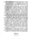
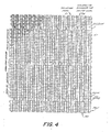
- Figs. 3 and 4 shows chip layouts for the conventional NAND stack ROM and the ROM embodying the present invention, respectively.
- a comparison of Figs. 3 and 4 indicates that since the virtual ground lines 40 run vertically through the array illustrated in Fig. 4, there is no need for the horizontal ground straps of N+ diffusion 44, shown in Fig. 3.
- the depletion mode transistors 14, 12 ⁇ are also eliminated.
- the depletion page decode transistor 14, 12 ⁇ in the conventional array and its longer array size add to column capacitance.
- the columns are 40% less capacitive as calculated using the same design rules and process parameters. This translates into a 12%-20% decrease in column charge-up time, depending upon the column operating voltage.
- adjacent columns in the array are tied to alternating sense amplifiers, D I and D ⁇ in the same way as X matrix ROM columns are organized. Interference between a column being selected and adjacent columns as well as sneak paths, which are common problems in X matrix ROM design, are significantly reduced.
- the multiplex transistors 38 are actuated by the same virtual ground lines 40 running vertically up the array. These metal virtual ground lines 40 do not increase the array's width since the array's horizontal axis is diffusion limited in the process technology used to develop the invention. In the conventional array, by contrast, the multiplexer is gated by lines running horizontally along the top of the array, using extra chip area. Because of the dual purpose virtual ground lines 40, a column in the array of Fig. 2 may have only one multiplexing transistor 34, 34 ⁇ to pass before the input of its sense amplifier, yet a 256K chip may have as few as one sense amplifier per output without increasing chip size.
- the array design of figs. 2 and 4 is technology independent. While the circuit disclosed herein is a CMOS implementation of an array of the present invention, it should be appreciated that the same concepts can be used in conjunction with an NMOS implementation. The design now proposed will reduce power consumption in NMOS ROMs which limit multiplexing at the top of the array by using more than one sense amplifier per output.
- the virtual ground NAND stack ROM design described with reference to Figs. 2 and 4 substantially reduces array size and column capacitance, hence decreasing total chip area and column charge-up time. It also combines the advantages of single transistor multiplexing at the top of the array with the lower power consumption of few sense amplifiers, without increasing the area of the circuitry peripheral to the array.
- the implementation of the design embodying the present invention is expected to significantly improve wafer yields.
Landscapes
- Engineering & Computer Science (AREA)
- Microelectronics & Electronic Packaging (AREA)
- Read Only Memory (AREA)
- Semiconductor Memories (AREA)
Applications Claiming Priority (2)
| Application Number | Priority Date | Filing Date | Title |
|---|---|---|---|
| US383787A | 1987-01-16 | 1987-01-16 | |
| US3837 | 1987-01-16 |
Publications (3)
| Publication Number | Publication Date |
|---|---|
| EP0275212A2 true EP0275212A2 (de) | 1988-07-20 |
| EP0275212A3 EP0275212A3 (en) | 1990-07-11 |
| EP0275212B1 EP0275212B1 (de) | 1993-08-04 |
Family
ID=21707824
Family Applications (1)
| Application Number | Title | Priority Date | Filing Date |
|---|---|---|---|
| EP88300339A Expired - Lifetime EP0275212B1 (de) | 1987-01-16 | 1988-01-15 | NAND-Stapelfestwertspeicher |
Country Status (3)
| Country | Link |
|---|---|
| EP (1) | EP0275212B1 (de) |
| DE (1) | DE3882720T2 (de) |
| IL (1) | IL85117A (de) |
Cited By (2)
| Publication number | Priority date | Publication date | Assignee | Title |
|---|---|---|---|---|
| EP0453206A3 (de) * | 1990-04-14 | 1994-02-23 | Nec Corp | |
| EP0822558A3 (de) * | 1996-07-30 | 2003-07-30 | NEC Corporation | Nichtflüchtige Halbleiterspeicheranordnung mit hoher Geschwindigkeit und niedrigem Verbrauch |
Family Cites Families (2)
| Publication number | Priority date | Publication date | Assignee | Title |
|---|---|---|---|---|
| US4489400A (en) * | 1982-03-01 | 1984-12-18 | Texas Instruments Incorporated | Serially banked read only memory |
| US4570239A (en) * | 1983-01-24 | 1986-02-11 | Motorola, Inc. | Series read-only-memory having capacitive bootstrap precharging circuitry |
-
1988
- 1988-01-15 DE DE88300339T patent/DE3882720T2/de not_active Expired - Fee Related
- 1988-01-15 EP EP88300339A patent/EP0275212B1/de not_active Expired - Lifetime
- 1988-01-17 IL IL85117A patent/IL85117A/xx not_active IP Right Cessation
Cited By (2)
| Publication number | Priority date | Publication date | Assignee | Title |
|---|---|---|---|---|
| EP0453206A3 (de) * | 1990-04-14 | 1994-02-23 | Nec Corp | |
| EP0822558A3 (de) * | 1996-07-30 | 2003-07-30 | NEC Corporation | Nichtflüchtige Halbleiterspeicheranordnung mit hoher Geschwindigkeit und niedrigem Verbrauch |
Also Published As
| Publication number | Publication date |
|---|---|
| DE3882720D1 (de) | 1993-09-09 |
| EP0275212B1 (de) | 1993-08-04 |
| DE3882720T2 (de) | 1993-11-18 |
| IL85117A0 (en) | 1988-06-30 |
| EP0275212A3 (en) | 1990-07-11 |
| IL85117A (en) | 1991-06-30 |
Similar Documents
| Publication | Publication Date | Title |
|---|---|---|
| US4980861A (en) | NAND stack ROM | |
| US6961272B2 (en) | Physically alternating sense amplifier activation | |
| US4485460A (en) | ROM coupling reduction circuitry | |
| JP3364235B2 (ja) | リードオンリメモリ集積回路 | |
| US5986914A (en) | Active hierarchical bitline memory architecture | |
| KR930006842B1 (ko) | 반도체 집적회로 | |
| JP3104319B2 (ja) | 不揮発性記憶装置 | |
| US4493056A (en) | RAM Utilizing offset contact regions for increased storage capacitance | |
| US4739497A (en) | Semiconductor memory | |
| JPH03171495A (ja) | 論理アレイのビット線セグメンテーション | |
| JPH0120515B2 (de) | ||
| GB1566221A (en) | Integrated circuit for random access memory chip | |
| US4758990A (en) | Resetting arrangement for a semiconductor integrated circuit device having semiconductor memory | |
| US5537346A (en) | Semiconductor memory device obtaining high bandwidth and signal line layout method thereof | |
| US4554646A (en) | Semiconductor memory device | |
| JPS6363193A (ja) | 集積メモリ回路 | |
| US4290120A (en) | Circuit arrangement for reading out and regenerating items of information stored in one-transistor storage elements | |
| US4480320A (en) | Compact ROM with reduced access time | |
| EP0450516B1 (de) | Halbleiterspeicher | |
| JPH0762960B2 (ja) | 半導体回路 | |
| EP0275212A2 (de) | NAND-Stapelfestwertspeicher | |
| US4901285A (en) | High density read-only memory | |
| JP2001256789A (ja) | 半導体集積回路 | |
| US20040119105A1 (en) | Ferroelectric memory | |
| EP0622801A2 (de) | Hierarchische Bitleitung-Speicher-Architektur |
Legal Events
| Date | Code | Title | Description |
|---|---|---|---|
| PUAI | Public reference made under article 153(3) epc to a published international application that has entered the european phase |
Free format text: ORIGINAL CODE: 0009012 |
|
| AK | Designated contracting states |
Kind code of ref document: A2 Designated state(s): BE CH DE FR GB IT LI NL SE |
|
| PUAL | Search report despatched |
Free format text: ORIGINAL CODE: 0009013 |
|
| AK | Designated contracting states |
Kind code of ref document: A3 Designated state(s): BE CH DE FR GB IT LI NL SE |
|
| 17P | Request for examination filed |
Effective date: 19901220 |
|
| 17Q | First examination report despatched |
Effective date: 19920218 |
|
| GRAA | (expected) grant |
Free format text: ORIGINAL CODE: 0009210 |
|
| AK | Designated contracting states |
Kind code of ref document: B1 Designated state(s): BE CH DE FR GB IT LI NL SE |
|
| PG25 | Lapsed in a contracting state [announced via postgrant information from national office to epo] |
Ref country code: IT Free format text: LAPSE BECAUSE OF FAILURE TO SUBMIT A TRANSLATION OF THE DESCRIPTION OR TO PAY THE FEE WITHIN THE PRE;WARNING: LAPSES OF ITALIAN PATENTS WITH EFFECTIVE DATE BEFORE 2007 MAY HAVE OCCURRED AT ANY TIME BEFORE 2007. THE CORRECT EFFECTIVE DATE MAY BE DIFFERENT FROM THE ONE RECORDED.SCRIBED TIME-LIMIT Effective date: 19930804 Ref country code: CH Effective date: 19930804 Ref country code: NL Effective date: 19930804 Ref country code: LI Effective date: 19930804 Ref country code: BE Effective date: 19930804 Ref country code: SE Effective date: 19930804 |
|
| REF | Corresponds to: |
Ref document number: 3882720 Country of ref document: DE Date of ref document: 19930909 |
|
| ET | Fr: translation filed | ||
| REG | Reference to a national code |
Ref country code: CH Ref legal event code: PL |
|
| PG25 | Lapsed in a contracting state [announced via postgrant information from national office to epo] |
Ref country code: GB Effective date: 19940115 |
|
| NLV1 | Nl: lapsed or annulled due to failure to fulfill the requirements of art. 29p and 29m of the patents act | ||
| PLBE | No opposition filed within time limit |
Free format text: ORIGINAL CODE: 0009261 |
|
| STAA | Information on the status of an ep patent application or granted ep patent |
Free format text: STATUS: NO OPPOSITION FILED WITHIN TIME LIMIT |
|
| 26N | No opposition filed | ||
| GBPC | Gb: european patent ceased through non-payment of renewal fee |
Effective date: 19940115 |
|
| PG25 | Lapsed in a contracting state [announced via postgrant information from national office to epo] |
Ref country code: FR Effective date: 19940930 |
|
| PGFP | Annual fee paid to national office [announced via postgrant information from national office to epo] |
Ref country code: DE Payment date: 19940930 Year of fee payment: 7 |
|
| REG | Reference to a national code |
Ref country code: FR Ref legal event code: ST |
|
| PG25 | Lapsed in a contracting state [announced via postgrant information from national office to epo] |
Ref country code: DE Effective date: 19951003 |
|
| P01 | Opt-out of the competence of the unified patent court (upc) registered |
Effective date: 20230520 |