EP0276703A2 - Thyristor de type zéro croisement - Google Patents
Thyristor de type zéro croisement Download PDFInfo
- Publication number
- EP0276703A2 EP0276703A2 EP88100533A EP88100533A EP0276703A2 EP 0276703 A2 EP0276703 A2 EP 0276703A2 EP 88100533 A EP88100533 A EP 88100533A EP 88100533 A EP88100533 A EP 88100533A EP 0276703 A2 EP0276703 A2 EP 0276703A2
- Authority
- EP
- European Patent Office
- Prior art keywords
- thyristor
- type
- layer
- emitter layer
- zero
- Prior art date
- Legal status (The legal status is an assumption and is not a legal conclusion. Google has not performed a legal analysis and makes no representation as to the accuracy of the status listed.)
- Granted
Links
- 239000000758 substrate Substances 0.000 claims abstract description 33
- 239000004065 semiconductor Substances 0.000 claims abstract description 23
- 230000003071 parasitic effect Effects 0.000 claims description 15
- 239000012535 impurity Substances 0.000 claims description 4
- 230000001629 suppression Effects 0.000 claims 4
- 230000006870 function Effects 0.000 description 13
- 230000001960 triggered effect Effects 0.000 description 8
- VMXJCRHCUWKQCB-UHFFFAOYSA-N NPNP Chemical group NPNP VMXJCRHCUWKQCB-UHFFFAOYSA-N 0.000 description 4
- 230000004048 modification Effects 0.000 description 3
- 238000012986 modification Methods 0.000 description 3
- 230000035945 sensitivity Effects 0.000 description 3
- 229910052782 aluminium Inorganic materials 0.000 description 2
- XAGFODPZIPBFFR-UHFFFAOYSA-N aluminium Chemical compound [Al] XAGFODPZIPBFFR-UHFFFAOYSA-N 0.000 description 2
- 230000003321 amplification Effects 0.000 description 2
- 239000003990 capacitor Substances 0.000 description 2
- 230000000694 effects Effects 0.000 description 2
- 230000002708 enhancing effect Effects 0.000 description 2
- 238000000034 method Methods 0.000 description 2
- 238000003199 nucleic acid amplification method Methods 0.000 description 2
- 230000015556 catabolic process Effects 0.000 description 1
- 239000002131 composite material Substances 0.000 description 1
- 238000010276 construction Methods 0.000 description 1
- 230000001419 dependent effect Effects 0.000 description 1
- 238000010586 diagram Methods 0.000 description 1
- 238000000605 extraction Methods 0.000 description 1
- 230000007257 malfunction Effects 0.000 description 1
- 238000004519 manufacturing process Methods 0.000 description 1
- 229910052751 metal Inorganic materials 0.000 description 1
- 239000002184 metal Substances 0.000 description 1
- 229920006395 saturated elastomer Polymers 0.000 description 1
Images



Classifications
-
- H—ELECTRICITY
- H10—SEMICONDUCTOR DEVICES; ELECTRIC SOLID-STATE DEVICES NOT OTHERWISE PROVIDED FOR
- H10D—INORGANIC ELECTRIC SEMICONDUCTOR DEVICES
- H10D18/00—Thyristors
- H10D18/221—Thyristors having amplifying gate structures, e.g. cascade configurations
Definitions
- a zero-crossing type thyristor is advantageously used, for the reason of reduced noise, as a power control switch provided at the final stage of a conventional temperature adjusting device, various industrial equipment, and the like.
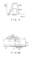
- a zero-crossing thyristor can be triggered only when a voltage (anode-cathode voltage) applied between the main electrodes is within a specified narrow voltage range which includes a zero-crossing voltage.
- the gate control element is formed of a bipolar or MOS transistor structure such as is disclosed in Japanese Patent Disclosures No. 60-74678 and No. 60-149164.
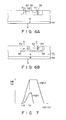
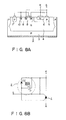
- Base layer 16 of NPN transistor Q7 corresponding to the gate of the second parasitic thyristor is connected to emitter layer 21 of transistor Q7 via metal electrode 23. This prevents the second parasitic thyristor to be triggered, thus keeping the same in the OFF state. Unless the second parasitic thyristor is turned on, the first parasitic thyristor including PNP transistor Q6 cannot be turned on.
Landscapes
- Thyristors (AREA)
- Thyristor Switches And Gates (AREA)
Applications Claiming Priority (2)
| Application Number | Priority Date | Filing Date | Title |
|---|---|---|---|
| JP14231/87 | 1987-01-26 | ||
| JP62014231A JPS63182861A (ja) | 1987-01-26 | 1987-01-26 | ゼロクロス型サイリスタ |
Publications (3)
| Publication Number | Publication Date |
|---|---|
| EP0276703A2 true EP0276703A2 (fr) | 1988-08-03 |
| EP0276703A3 EP0276703A3 (en) | 1988-11-02 |
| EP0276703B1 EP0276703B1 (fr) | 1993-05-05 |
Family
ID=11855298
Family Applications (1)
| Application Number | Title | Priority Date | Filing Date |
|---|---|---|---|
| EP88100533A Expired - Lifetime EP0276703B1 (fr) | 1987-01-26 | 1988-01-15 | Thyristor de type zéro croisement |
Country Status (4)
| Country | Link |
|---|---|
| US (1) | US4956690A (fr) |
| EP (1) | EP0276703B1 (fr) |
| JP (1) | JPS63182861A (fr) |
| DE (1) | DE3880699T2 (fr) |
Cited By (2)
| Publication number | Priority date | Publication date | Assignee | Title |
|---|---|---|---|---|
| DE4142807A1 (de) * | 1990-12-28 | 1992-07-02 | Fuji Electric Co Ltd | Mos gesteuerter thyristor und verfahren zu seiner herstellung |
| US5793065A (en) * | 1990-09-17 | 1998-08-11 | Kabushiki Kaisha Toshiba | Insulated-gate thyristor |
Families Citing this family (13)
| Publication number | Priority date | Publication date | Assignee | Title |
|---|---|---|---|---|
| US5294816A (en) * | 1992-06-10 | 1994-03-15 | North Carolina State University At Raleigh | Unit cell arrangement for emitter switched thyristor with base resistance control |
| US5198687A (en) * | 1992-07-23 | 1993-03-30 | Baliga Bantval J | Base resistance controlled thyristor with single-polarity turn-on and turn-off control |
| FR2697674B1 (fr) * | 1992-10-29 | 1995-01-13 | Sgs Thomson Microelectronics | Thyristor et assemblage de thyristors à cathode commune. |
| US5293054A (en) * | 1992-11-23 | 1994-03-08 | North Carolina State University At Raleigh | Emitter switched thyristor without parasitic thyristor latch-up susceptibility |
| US5306930A (en) * | 1992-12-14 | 1994-04-26 | North Carolina State University At Raleigh | Emitter switched thyristor with buried dielectric layer |
| US5396087A (en) * | 1992-12-14 | 1995-03-07 | North Carolina State University | Insulated gate bipolar transistor with reduced susceptibility to parasitic latch-up |
| US5241194A (en) * | 1992-12-14 | 1993-08-31 | North Carolina State University At Raleigh | Base resistance controlled thyristor with integrated single-polarity gate control |
| FR2708811B1 (fr) * | 1993-08-06 | 1995-10-20 | Sgs Thomson Microelectronics | Thyristor à amplification de gachette à courant de maintien accru. |
| US5493134A (en) * | 1994-11-14 | 1996-02-20 | North Carolina State University | Bidirectional AC switching device with MOS-gated turn-on and turn-off control |
| FR2734429B1 (fr) * | 1995-05-19 | 1997-08-01 | Sgs Thomson Microelectronics | Module interrupteur et d'alimentation-application au demarrage d'un tube fluorescent |
| JP4126872B2 (ja) * | 2000-12-12 | 2008-07-30 | サンケン電気株式会社 | 定電圧ダイオード |
| DE102016204699B4 (de) | 2015-04-13 | 2020-07-30 | Infineon Technologies Ag | Schutzvorrichtungen mit Trigger-Vorrichtungen und Verfahren zu deren Bildung |
| US10741548B2 (en) * | 2015-04-13 | 2020-08-11 | Infineon Technologies Ag | Protection devices with trigger devices and methods of formation thereof |
Family Cites Families (5)
| Publication number | Priority date | Publication date | Assignee | Title |
|---|---|---|---|---|
| GB1194427A (en) * | 1967-08-09 | 1970-06-10 | Associated Semiconductor Mft | Improvements in Semiconductor Integrated Circuits |
| US4050083A (en) * | 1976-09-22 | 1977-09-20 | Cutler-Hammer, Inc. | Integrated thermally sensitive power switching semiconductor device, including a thermally self-protected version |
| US4529998A (en) * | 1977-12-14 | 1985-07-16 | Eaton Corporation | Amplified gate thyristor with non-latching amplified control transistors across base layers |
| JPS6074678A (ja) * | 1983-09-30 | 1985-04-26 | Toshiba Corp | 半導体装置 |
| JPH0697692B2 (ja) * | 1984-01-17 | 1994-11-30 | 株式会社東芝 | 半導体装置 |
-
1987
- 1987-01-26 JP JP62014231A patent/JPS63182861A/ja active Granted
-
1988
- 1988-01-15 EP EP88100533A patent/EP0276703B1/fr not_active Expired - Lifetime
- 1988-01-15 DE DE8888100533T patent/DE3880699T2/de not_active Expired - Lifetime
-
1990
- 1990-01-26 US US07/471,025 patent/US4956690A/en not_active Expired - Lifetime
Cited By (3)
| Publication number | Priority date | Publication date | Assignee | Title |
|---|---|---|---|---|
| US5793065A (en) * | 1990-09-17 | 1998-08-11 | Kabushiki Kaisha Toshiba | Insulated-gate thyristor |
| US6236069B1 (en) | 1990-09-17 | 2001-05-22 | Kabushiki Kaisha Toshiba | Insulated-gate thyristor |
| DE4142807A1 (de) * | 1990-12-28 | 1992-07-02 | Fuji Electric Co Ltd | Mos gesteuerter thyristor und verfahren zu seiner herstellung |
Also Published As
| Publication number | Publication date |
|---|---|
| EP0276703A3 (en) | 1988-11-02 |
| EP0276703B1 (fr) | 1993-05-05 |
| US4956690A (en) | 1990-09-11 |
| JPS63182861A (ja) | 1988-07-28 |
| DE3880699D1 (de) | 1993-06-09 |
| JPH0449266B2 (fr) | 1992-08-11 |
| DE3880699T2 (de) | 1993-08-19 |
Similar Documents
| Publication | Publication Date | Title |
|---|---|---|
| EP0276703B1 (fr) | Thyristor de type zéro croisement | |
| US5500546A (en) | ESD protection circuits using Zener diodes | |
| US5808342A (en) | Bipolar SCR triggering for ESD protection of high speed bipolar/BiCMOS circuits | |
| US4567500A (en) | Semiconductor structure for protecting integrated circuit devices | |
| US6919604B2 (en) | Silicon controlled rectifier structure with guard ring controlled circuit | |
| US5164802A (en) | Power vdmosfet with schottky on lightly doped drain of lateral driver fet | |
| US5548134A (en) | Device for the protection of an integrated circuit against electrostatic discharges | |
| US5780905A (en) | Asymmetrical, bidirectional triggering ESD structure | |
| US5166089A (en) | Method of making electrostatic discharge protection for semiconductor input devices | |
| US4672584A (en) | CMOS integrated circuit | |
| US6674129B1 (en) | ESD diode structure | |
| JPS5990120A (ja) | 保護回路 | |
| US4543593A (en) | Semiconductor protective device | |
| EP0287856A1 (fr) | Dispositif semi-conducteur de commutation, bidirectionnel, à commande par porte | |
| US5148250A (en) | Bipolar transistor as protective element for integrated circuits | |
| US5051612A (en) | Prevention of parasitic mechanisms in junction isolated devices | |
| US4939564A (en) | Gate-controlled bidirectional semiconductor switching device with rectifier | |
| JPH07183517A (ja) | 双方向性スイッチ | |
| US3230429A (en) | Integrated transistor, diode and resistance semiconductor network | |
| US6188267B1 (en) | Normally conducting dual thyristor | |
| GB2286923A (en) | ESD input protection arrangement | |
| US7262442B2 (en) | Triac operating in quadrants Q1 and Q4 | |
| US4969024A (en) | Metal-oxide-semiconductor device | |
| CN115966567A (zh) | 静电放电保护装置 | |
| KR100347397B1 (ko) | 반도체 집적회로용 입출력 보호 장치 |
Legal Events
| Date | Code | Title | Description |
|---|---|---|---|
| PUAI | Public reference made under article 153(3) epc to a published international application that has entered the european phase |
Free format text: ORIGINAL CODE: 0009012 |
|
| 17P | Request for examination filed |
Effective date: 19880212 |
|
| AK | Designated contracting states |
Kind code of ref document: A2 Designated state(s): DE FR GB |
|
| PUAL | Search report despatched |
Free format text: ORIGINAL CODE: 0009013 |
|
| AK | Designated contracting states |
Kind code of ref document: A3 Designated state(s): DE FR GB |
|
| 17Q | First examination report despatched |
Effective date: 19920508 |
|
| GRAA | (expected) grant |
Free format text: ORIGINAL CODE: 0009210 |
|
| AK | Designated contracting states |
Kind code of ref document: B1 Designated state(s): DE FR GB |
|
| REF | Corresponds to: |
Ref document number: 3880699 Country of ref document: DE Date of ref document: 19930609 |
|
| ET | Fr: translation filed | ||
| PLBE | No opposition filed within time limit |
Free format text: ORIGINAL CODE: 0009261 |
|
| STAA | Information on the status of an ep patent application or granted ep patent |
Free format text: STATUS: NO OPPOSITION FILED WITHIN TIME LIMIT |
|
| 26N | No opposition filed | ||
| REG | Reference to a national code |
Ref country code: GB Ref legal event code: 746 Effective date: 19981002 |
|
| REG | Reference to a national code |
Ref country code: FR Ref legal event code: D6 |
|
| REG | Reference to a national code |
Ref country code: GB Ref legal event code: IF02 |
|
| PGFP | Annual fee paid to national office [announced via postgrant information from national office to epo] |
Ref country code: GB Payment date: 20070110 Year of fee payment: 20 |
|
| PGFP | Annual fee paid to national office [announced via postgrant information from national office to epo] |
Ref country code: DE Payment date: 20070111 Year of fee payment: 20 |
|
| REG | Reference to a national code |
Ref country code: GB Ref legal event code: PE20 |
|
| PGFP | Annual fee paid to national office [announced via postgrant information from national office to epo] |
Ref country code: FR Payment date: 20070109 Year of fee payment: 20 |
|
| PG25 | Lapsed in a contracting state [announced via postgrant information from national office to epo] |
Ref country code: GB Free format text: LAPSE BECAUSE OF EXPIRATION OF PROTECTION Effective date: 20080114 |