EP0278460A2 - Vorrichtung zur Handhabung von Wafern - Google Patents
Vorrichtung zur Handhabung von Wafern Download PDFInfo
- Publication number
- EP0278460A2 EP0278460A2 EP88101809A EP88101809A EP0278460A2 EP 0278460 A2 EP0278460 A2 EP 0278460A2 EP 88101809 A EP88101809 A EP 88101809A EP 88101809 A EP88101809 A EP 88101809A EP 0278460 A2 EP0278460 A2 EP 0278460A2
- Authority
- EP
- European Patent Office
- Prior art keywords
- plane
- support arm
- wafer
- transfer member
- semiconductor wafer
- Prior art date
- Legal status (The legal status is an assumption and is not a legal conclusion. Google has not performed a legal analysis and makes no representation as to the accuracy of the status listed.)
- Granted
Links
Images


Classifications
-
- H—ELECTRICITY
- H10—SEMICONDUCTOR DEVICES; ELECTRIC SOLID-STATE DEVICES NOT OTHERWISE PROVIDED FOR
- H10P—GENERIC PROCESSES OR APPARATUS FOR THE MANUFACTURE OR TREATMENT OF DEVICES COVERED BY CLASS H10
- H10P72/00—Handling or holding of wafers, substrates or devices during manufacture or treatment thereof
- H10P72/30—Handling or holding of wafers, substrates or devices during manufacture or treatment thereof for conveying, e.g. between different workstations
- H10P72/32—Handling or holding of wafers, substrates or devices during manufacture or treatment thereof for conveying, e.g. between different workstations between different workstations
- H10P72/3202—Mechanical details, e.g. rollers or belts
-
- H—ELECTRICITY
- H10—SEMICONDUCTOR DEVICES; ELECTRIC SOLID-STATE DEVICES NOT OTHERWISE PROVIDED FOR
- H10P—GENERIC PROCESSES OR APPARATUS FOR THE MANUFACTURE OR TREATMENT OF DEVICES COVERED BY CLASS H10
- H10P72/00—Handling or holding of wafers, substrates or devices during manufacture or treatment thereof
- H10P72/70—Handling or holding of wafers, substrates or devices during manufacture or treatment thereof for supporting or gripping
- H10P72/78—Handling or holding of wafers, substrates or devices during manufacture or treatment thereof for supporting or gripping using vacuum or suction, e.g. Bernoulli chucks
-
- Y—GENERAL TAGGING OF NEW TECHNOLOGICAL DEVELOPMENTS; GENERAL TAGGING OF CROSS-SECTIONAL TECHNOLOGIES SPANNING OVER SEVERAL SECTIONS OF THE IPC; TECHNICAL SUBJECTS COVERED BY FORMER USPC CROSS-REFERENCE ART COLLECTIONS [XRACs] AND DIGESTS
- Y10—TECHNICAL SUBJECTS COVERED BY FORMER USPC
- Y10S—TECHNICAL SUBJECTS COVERED BY FORMER USPC CROSS-REFERENCE ART COLLECTIONS [XRACs] AND DIGESTS
- Y10S414/00—Material or article handling
- Y10S414/135—Associated with semiconductor wafer handling
- Y10S414/136—Associated with semiconductor wafer handling including wafer orienting means
-
- Y—GENERAL TAGGING OF NEW TECHNOLOGICAL DEVELOPMENTS; GENERAL TAGGING OF CROSS-SECTIONAL TECHNOLOGIES SPANNING OVER SEVERAL SECTIONS OF THE IPC; TECHNICAL SUBJECTS COVERED BY FORMER USPC CROSS-REFERENCE ART COLLECTIONS [XRACs] AND DIGESTS
- Y10—TECHNICAL SUBJECTS COVERED BY FORMER USPC
- Y10S—TECHNICAL SUBJECTS COVERED BY FORMER USPC CROSS-REFERENCE ART COLLECTIONS [XRACs] AND DIGESTS
- Y10S414/00—Material or article handling
- Y10S414/135—Associated with semiconductor wafer handling
- Y10S414/141—Associated with semiconductor wafer handling includes means for gripping wafer
Definitions
- This invention pertains generally to the field of automated handling of semiconductor wafers during the manufacture of semiconductor chips and more particularly to the precise positioning of a chip in different planes.
- This apparatus comprises a wafer support arm which is carried by a transfer member and is rotatable in a first plane between an established "start” position and an intermediate position. Means are provided for rotating the transfer member to position the wafer support arm in a second plane, and means are provided for establishing a "finish" position. The start and the finish positions are substantially the same, relative to the transfer member.
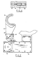
- Fig. 1 illustrates schematically the manner in which a wafer W is moved from a start position I in a horizontal plane to a final position IV in a vertical plane.
- a fixed housing 10 carries a motor 12 which, through a gear train (not shown) enclosed in housing 10, drives an output shaft 14.
- a transfer member 16 Mounted to the output shaft 14 for rotation therewith is a transfer member 16.
- Transfer member 16 also carries a motor 18 which, through a similarly enclosed gear train, drives an output shaft 20.
- Mounted to the shaft 20 is a conventional wafer support arm 22, the end of which is C-shaped and includes a vacuum groove 24 for firmly holding a wafer W.
- Transfer of the wafer W begins with motor 18 turning the shaft 20 to retract the wafer support arm 22 to an intermediate position II. This move is necessary to permit the wafer W to avoid intervening obstructions between the initial position I and the final position IV.
- the motor 12 is then actuated so as to turn the shaft 14 and rotate the transfer member 16, together with its motor 18 and its support arm 22, clockwise as viewed in Fig. 1 to the dotted line position 16 ⁇ to thereby locate the arm 22 in position III.
- the motor 18 ⁇ is once more actuated to return the arm 22 to essentially the same initial position, relative to the transfer members position 16 ⁇ , but otherwise into a final position IV in the vertical plane.
- FIG. 2 A specific application of the principle illustrated in Fig. 1 will now be described in detail, referring to Figs. 2 - 5.
- a support 26 which supports a base 28 and motor 30.
- the base 28 encloses a gear train comprising a worm 32 mounted on an input shaft 34 and a sector gear 36 mounted on an output shaft 38.
- the input shaft 34 is driven by the motor 30 through a flexible coupling 40.
- Transfer member 44 is mounted to the shaft 38.
- Arm 42 and transfer member 44 are preferably made of one integrated piece.
- Transfer member 44 carries a housing 45 which encloses a gear train comprising worm 46 and gear 48. This gear train is driven by a motor 50 (Fig. 4) through a flexible coupling 52.
- the output shaft 54 extends through the opposite sides of the housing 45 and is connected to a pair of hub arms 56.
- bracket 58 carries at its lower end a wafer support arm 60.
- Wafer support arm 60 is of conventional construction, having a C-shaped end defining a vacuum groove 62 as seen in Fig. 2. A vacuum is supplied to vacuum groove 62 by vacuum inlet 61 on bracket 58.
- a ball mount bracket 64 (Fig. 2) which carries a tooling ball 66.
- a block 68 Extending upwardly from the bracket 58 is a block 68 into which is threaded an initial placement rod 70 which defines at its end a concave cone 72 (Fig. 6).
- a final placement rod 71 similar to initial placement rod 70, extends through bracket 58.
- the cone 72 mates with the initial placement ball 66 to provide a very accurate initial starting point for movement of the arm 60.
- a precise final position for arm 60 is provided by a similar final placement ball 74 which is carried by the base 28 on its lower opposite side, as will be seen in Fig. 5.
- Figs. 2 and 3 illustrate the initial position of the arm 60.
- the motor 50 begins to turn and, through the worm 46 and the gear 48, rotates the hub arms 56 and the associated elements, including the wafer support arm 60, counter-clockwise as viewed from above to an intermediate position illustrated in Fig. 4.
- the exact position where the wafer support arm 60 stops is not critical. The only critical positions are the initial and final ones and these are established by the two ball and cone stops. Retraction of the arm 60 to the Fig. 4 position assures avoiding contact with underlying mechanisms during the downward rotation.
- the motor 30 next begins to turn.
- This motor through the worm 32 and the sector gear 36, rotates the transfer member 44 and the entire mechanism associated with it including housing 45, the gear train 46, 48 and the motor 50 downwardly the counter-clockwise as viewed in Fig. 3.
- the arm 60 is positioned in a vertical plane as seen in phantom in Fig. 5.
- the motor 50 operates in the reverse of this initial motion to thereby return the arm 60 to essentially the same position relative to the transfer member 44.
- the wafer support arm 60 is now positioned such that the cone in the final placement rod 71 seats against the final placement ball 74, thereby insuring accurate final placement.
Landscapes
- Container, Conveyance, Adherence, Positioning, Of Wafer (AREA)
- Feeding Of Articles By Means Other Than Belts Or Rollers (AREA)
Applications Claiming Priority (2)
| Application Number | Priority Date | Filing Date | Title |
|---|---|---|---|
| US07/012,537 US4778332A (en) | 1987-02-09 | 1987-02-09 | Wafer flip apparatus |
| US12537 | 1998-01-23 |
Publications (3)
| Publication Number | Publication Date |
|---|---|
| EP0278460A2 true EP0278460A2 (de) | 1988-08-17 |
| EP0278460A3 EP0278460A3 (en) | 1990-07-18 |
| EP0278460B1 EP0278460B1 (de) | 1995-01-18 |
Family
ID=21755435
Family Applications (1)
| Application Number | Title | Priority Date | Filing Date |
|---|---|---|---|
| EP88101809A Expired - Lifetime EP0278460B1 (de) | 1987-02-09 | 1988-02-08 | Vorrichtung zur Handhabung von Wafern |
Country Status (6)
| Country | Link |
|---|---|
| US (1) | US4778332A (de) |
| EP (1) | EP0278460B1 (de) |
| JP (1) | JP2550130B2 (de) |
| KR (1) | KR970000967B1 (de) |
| CA (1) | CA1278879C (de) |
| DE (1) | DE3852770T2 (de) |
Cited By (2)
| Publication number | Priority date | Publication date | Assignee | Title |
|---|---|---|---|---|
| EP0361959A3 (de) * | 1988-09-30 | 1990-10-17 | Canon Kabushiki Kaisha | Transportvorrichtung für Substrate |
| NL1003342C2 (nl) * | 1996-06-14 | 1997-12-17 | Fico Bv | Inrichting voor het gelijktijdig verplaatsen en wijzigen van de oriënta- tie van ten minste één drager voor electronische componenten. |
Families Citing this family (34)
| Publication number | Priority date | Publication date | Assignee | Title |
|---|---|---|---|---|
| US5020789A (en) * | 1988-12-09 | 1991-06-04 | International Business Machines Corporation | Drive up teller machine |
| US5344521A (en) * | 1991-04-10 | 1994-09-06 | Canon Kabushiki Kaisha | Coating film separating device and coating film separation method using the device |
| US5154730A (en) * | 1991-05-17 | 1992-10-13 | Materials Research Corporation | Semiconductor wafer processing module having an inclined rotating wafer handling turret and a method of using the module |
| CH686445A5 (de) * | 1992-10-06 | 1996-03-29 | Balzers Hochvakuum | Kammer und Kammerkombination fuer eine Vakuumanlage und Verfahren zum Durchreichen mindestens eines Werkstueckes. |
| US5295777A (en) * | 1992-12-23 | 1994-03-22 | Materials Research Corporation | Wafer transport module with rotatable and horizontally extendable wafer holder |
| US5421889A (en) * | 1993-06-29 | 1995-06-06 | Tokyo Electron Limited | Method and apparatus for inverting samples in a process |
| KR0135802B1 (ko) * | 1994-07-11 | 1998-04-29 | 김광호 | 웨이퍼 운반장치 및 운반장치 제조방법 |
| US5507614A (en) * | 1995-03-02 | 1996-04-16 | Cybeq Systems | Holder mechanism for simultaneously tilting and rotating a wafer cassette |
| JPH08288355A (ja) * | 1995-04-12 | 1996-11-01 | Nikon Corp | 基板搬送装置 |
| JP3771320B2 (ja) * | 1996-03-29 | 2006-04-26 | コマツ電子金属株式会社 | 半導体ウェハの貼付方法及び貼付装置 |
| US5993148A (en) | 1997-07-22 | 1999-11-30 | Micron Technology, Inc. | Article transfer methods |
| US6183186B1 (en) | 1997-08-29 | 2001-02-06 | Daitron, Inc. | Wafer handling system and method |
| US5915910A (en) * | 1997-08-29 | 1999-06-29 | Daitron, Inc. | Semiconductor wafer transfer method and apparatus |
| WO2000078654A1 (en) * | 1999-06-17 | 2000-12-28 | Speedfam-Ipec Corporation | Improved wafer handling apparatus |
| US6239863B1 (en) | 1999-10-08 | 2001-05-29 | Silicon Valley Group, Inc. | Removable cover for protecting a reticle, system including and method of using the same |
| US6467827B1 (en) | 1999-10-30 | 2002-10-22 | Frank J. Ardezzone | IC wafer handling apparatus incorporating edge-gripping and pressure or vacuum driven end-effectors |
| KR100597035B1 (ko) * | 2001-03-01 | 2006-07-04 | 에이에스엠엘 네델란즈 비.브이. | 마스크핸들링방법, 마스크, 그를 위한 그리퍼를 포함하는기구 또는 장치, 디바이스 제조방법 및 그 디바이스 |
| US6695572B2 (en) * | 2001-09-28 | 2004-02-24 | Agere Systems Inc. | Method and apparatus for minimizing semiconductor wafer contamination |
| US6906783B2 (en) * | 2002-02-22 | 2005-06-14 | Asml Holding N.V. | System for using a two part cover for protecting a reticle |
| US6862817B1 (en) * | 2003-11-12 | 2005-03-08 | Asml Holding N.V. | Method and apparatus for kinematic registration of a reticle |
| US7993093B2 (en) * | 2004-09-15 | 2011-08-09 | Applied Materials, Inc. | Systems and methods for wafer translation |
| US7798764B2 (en) | 2005-12-22 | 2010-09-21 | Applied Materials, Inc. | Substrate processing sequence in a cartesian robot cluster tool |
| US20060130767A1 (en) | 2004-12-22 | 2006-06-22 | Applied Materials, Inc. | Purged vacuum chuck with proximity pins |
| US7651306B2 (en) | 2004-12-22 | 2010-01-26 | Applied Materials, Inc. | Cartesian robot cluster tool architecture |
| US7819079B2 (en) | 2004-12-22 | 2010-10-26 | Applied Materials, Inc. | Cartesian cluster tool configuration for lithography type processes |
| US7374391B2 (en) * | 2005-12-22 | 2008-05-20 | Applied Materials, Inc. | Substrate gripper for a substrate handling robot |
| DE102005050638B4 (de) * | 2005-10-20 | 2020-07-16 | Tdk Electronics Ag | Elektrisches Bauelement |
| JP4895635B2 (ja) * | 2006-02-20 | 2012-03-14 | セイコーインスツル株式会社 | 搬送装置 |
| US8376428B2 (en) | 2006-11-15 | 2013-02-19 | Dynamic Micro System Semiconductor Equipment GmbH | Integrated gripper for workpiece transfer |
| US20080166210A1 (en) * | 2007-01-05 | 2008-07-10 | Applied Materials, Inc. | Supinating cartesian robot blade |
| US20090065995A1 (en) * | 2007-09-11 | 2009-03-12 | Atmel Corporation | Ambidexturous Shuttle Spoon |
| JP2009105357A (ja) * | 2007-10-23 | 2009-05-14 | M Tec Kk | チップの搬送方法及び装置 |
| US9117856B2 (en) | 2011-07-06 | 2015-08-25 | Tel Nexx, Inc. | Substrate loader and unloader having an air bearing support |
| US11035591B2 (en) * | 2015-10-13 | 2021-06-15 | Corosolar Llc | Bearing assembly for solar trackers |
Family Cites Families (25)
| Publication number | Priority date | Publication date | Assignee | Title |
|---|---|---|---|---|
| US3437929A (en) * | 1965-08-05 | 1969-04-08 | Electroglas Inc | Automatically indexed probe assembly for testing semiconductor wafers and the like |
| US3499640A (en) * | 1967-08-03 | 1970-03-10 | Electroglas Inc | Chuck assembly for automatic wafer die sort machine |
| US3711081A (en) * | 1970-03-31 | 1973-01-16 | Ibm | Semiconductor wafer chuck |
| US3700228A (en) * | 1970-09-25 | 1972-10-24 | Robert E Peale | Adjustable axis work support |
| US3841499A (en) * | 1973-10-31 | 1974-10-15 | Armflex Inc | Work transfer apparatus |
| US3960277A (en) * | 1974-09-30 | 1976-06-01 | Flint Alan G | Mask plate handling apparatus |
| US4042122A (en) * | 1975-05-27 | 1977-08-16 | The Bendix Corporation | Reorientation device for an object manipulator |
| FR2352640A1 (fr) * | 1976-05-24 | 1977-12-23 | Bretagne Atel Chantiers | Telemanipulateur a faible encombrement |
| CA1034393A (en) * | 1976-10-13 | 1978-07-11 | Spar Aerospace Products Limited | Powered wrist joint |
| FR2388372A1 (fr) * | 1977-04-20 | 1978-11-17 | Thomson Csf | Platine a rattrapage de niveau et positionneur a indexation mecanique utilisant une telle platine |
| US4262891A (en) * | 1979-06-04 | 1981-04-21 | Kinney Charles G | Three dimensional positionable workpiece support table |
| FR2461556A1 (fr) * | 1979-07-18 | 1981-02-06 | Bretagne Atel Chantiers | Bras de manipulation a distance |
| JPS5912435B2 (ja) * | 1980-07-25 | 1984-03-23 | ファナック株式会社 | 工業用ロボットの安全機構 |
| JPS5912436B2 (ja) * | 1980-08-05 | 1984-03-23 | ファナック株式会社 | 工業用ロボットの安全機構 |
| JPS6039518B2 (ja) * | 1980-09-30 | 1985-09-06 | ファナック株式会社 | 工業用ロボットの手首機構 |
| AU546502B2 (en) * | 1981-07-31 | 1985-09-05 | Bird-Johnson Company | Mechanical wrist |
| US4568070A (en) * | 1981-09-15 | 1986-02-04 | Severt W | Positioning and turning apparatus |
| US4444492A (en) * | 1982-05-15 | 1984-04-24 | General Signal Corporation | Apparatus for projecting a series of images onto dies of a semiconductor wafer |
| GB2126559A (en) * | 1982-09-07 | 1984-03-28 | Itt | Manipulator apparatus |
| US4603897A (en) * | 1983-05-20 | 1986-08-05 | Poconics International, Inc. | Vacuum pickup apparatus |
| US4684312A (en) * | 1984-04-30 | 1987-08-04 | Westinghouse Electric Corp. | Robotic wrist |
| US4566726A (en) * | 1984-06-13 | 1986-01-28 | At&T Technologies, Inc. | Method and apparatus for handling semiconductor wafers |
| US4557514A (en) * | 1984-07-18 | 1985-12-10 | At&T Technologies, Inc. | Vacuum pick and place robotic hand |
| US4586743A (en) * | 1984-09-24 | 1986-05-06 | Intelledex Incorporated | Robotic gripper for disk-shaped objects |
| DD240166A1 (de) * | 1985-08-14 | 1986-10-22 | Karl Marx Stadt Tech Hochschul | Revolverkopf fuer industrieroboter |
-
1987
- 1987-02-09 US US07/012,537 patent/US4778332A/en not_active Expired - Lifetime
-
1988
- 1988-02-04 CA CA000558131A patent/CA1278879C/en not_active Expired - Lifetime
- 1988-02-08 DE DE3852770T patent/DE3852770T2/de not_active Expired - Lifetime
- 1988-02-08 EP EP88101809A patent/EP0278460B1/de not_active Expired - Lifetime
- 1988-02-09 KR KR1019880001178A patent/KR970000967B1/ko not_active Expired - Fee Related
- 1988-02-09 JP JP2670988A patent/JP2550130B2/ja not_active Expired - Lifetime
Cited By (3)
| Publication number | Priority date | Publication date | Assignee | Title |
|---|---|---|---|---|
| EP0361959A3 (de) * | 1988-09-30 | 1990-10-17 | Canon Kabushiki Kaisha | Transportvorrichtung für Substrate |
| NL1003342C2 (nl) * | 1996-06-14 | 1997-12-17 | Fico Bv | Inrichting voor het gelijktijdig verplaatsen en wijzigen van de oriënta- tie van ten minste één drager voor electronische componenten. |
| WO1997048125A1 (en) * | 1996-06-14 | 1997-12-18 | Fico B.V. | Device for simultaneous transport and change of orientation of at least one carrier for electronic components |
Also Published As
| Publication number | Publication date |
|---|---|
| US4778332A (en) | 1988-10-18 |
| CA1278879C (en) | 1991-01-08 |
| JP2550130B2 (ja) | 1996-11-06 |
| DE3852770T2 (de) | 1995-05-18 |
| KR880010475A (ko) | 1988-10-10 |
| EP0278460B1 (de) | 1995-01-18 |
| DE3852770D1 (de) | 1995-03-02 |
| KR970000967B1 (ko) | 1997-01-21 |
| EP0278460A3 (en) | 1990-07-18 |
| JPS6419741A (en) | 1989-01-23 |
Similar Documents
| Publication | Publication Date | Title |
|---|---|---|
| US4778332A (en) | Wafer flip apparatus | |
| US4808059A (en) | Apparatus and method for transferring workpieces | |
| EP0235047B1 (de) | Vorrichtung zur Bestückung mit Chips | |
| JPS63211645A (ja) | ウエハーを装着及び離脱する方法及び装置 | |
| EP4501537A1 (de) | Waferpoliersystem und ladeverfahren und verwendungsverfahren dafür | |
| JP2003531479A (ja) | 加工物の並列加工装置 | |
| US6066031A (en) | Wafer chamfering method and apparatus | |
| US6190118B1 (en) | Tilt mechanism for wafer cassette | |
| JPH05109866A (ja) | ウエハ移載ロボツト | |
| US4573261A (en) | Automatic assembling machine | |
| US20050183754A1 (en) | Apparatus for and method of cleaning substrate | |
| JPH07211766A (ja) | 中心合わせ装置 | |
| CN217009164U (zh) | 一种承载装置及检测设备 | |
| JP2811856B2 (ja) | 電子部品の実装装置及び実装方法 | |
| CN118952241A (zh) | 一种机械臂及其控制方法 | |
| JP4230740B2 (ja) | アライメント装置 | |
| JP2000182996A (ja) | ダイシング装置 | |
| KR100275129B1 (ko) | 웨이퍼의 프리얼라인먼트죤 및 식별번호 인식작업을 위한 위치조정장치 | |
| JP2625786B2 (ja) | 電子部品マウント装置 | |
| CN224137617U (zh) | 一种具备双工位交替曝光的曝光机输送平台 | |
| JP3342210B2 (ja) | ペレット移送装置 | |
| JPH0628225B2 (ja) | 露光方法 | |
| JPH041150Y2 (de) | ||
| JPH0628224B2 (ja) | 露光方法および装置 | |
| JPH1197329A (ja) | 基板処理装置 |
Legal Events
| Date | Code | Title | Description |
|---|---|---|---|
| PUAI | Public reference made under article 153(3) epc to a published international application that has entered the european phase |
Free format text: ORIGINAL CODE: 0009012 |
|
| AK | Designated contracting states |
Kind code of ref document: A2 Designated state(s): DE FR GB IT NL |
|
| PUAL | Search report despatched |
Free format text: ORIGINAL CODE: 0009013 |
|
| AK | Designated contracting states |
Kind code of ref document: A3 Designated state(s): DE FR GB IT NL |
|
| 17P | Request for examination filed |
Effective date: 19910118 |
|
| RAP1 | Party data changed (applicant data changed or rights of an application transferred) |
Owner name: SVG LITHOGRAPHY SYSTEMS, INC. |
|
| 17Q | First examination report despatched |
Effective date: 19921104 |
|
| GRAA | (expected) grant |
Free format text: ORIGINAL CODE: 0009210 |
|
| AK | Designated contracting states |
Kind code of ref document: B1 Designated state(s): DE FR GB IT NL |
|
| ITF | It: translation for a ep patent filed | ||
| REF | Corresponds to: |
Ref document number: 3852770 Country of ref document: DE Date of ref document: 19950302 |
|
| ET | Fr: translation filed | ||
| NLT2 | Nl: modifications (of names), taken from the european patent patent bulletin |
Owner name: SVG LITHOGRAPHY SYSTEMS, INC. |
|
| PLBE | No opposition filed within time limit |
Free format text: ORIGINAL CODE: 0009261 |
|
| 26N | No opposition filed | ||
| REG | Reference to a national code |
Ref country code: GB Ref legal event code: IF02 |
|
| PGFP | Annual fee paid to national office [announced via postgrant information from national office to epo] |
Ref country code: NL Payment date: 20070213 Year of fee payment: 20 |
|
| PGFP | Annual fee paid to national office [announced via postgrant information from national office to epo] |
Ref country code: GB Payment date: 20070216 Year of fee payment: 20 Ref country code: DE Payment date: 20070216 Year of fee payment: 20 |
|
| PGFP | Annual fee paid to national office [announced via postgrant information from national office to epo] |
Ref country code: IT Payment date: 20070613 Year of fee payment: 20 |
|
| REG | Reference to a national code |
Ref country code: GB Ref legal event code: PE20 |
|
| NLV7 | Nl: ceased due to reaching the maximum lifetime of a patent |
Effective date: 20080208 |
|
| PG25 | Lapsed in a contracting state [announced via postgrant information from national office to epo] |
Ref country code: NL Free format text: LAPSE BECAUSE OF EXPIRATION OF PROTECTION Effective date: 20080208 |
|
| PGFP | Annual fee paid to national office [announced via postgrant information from national office to epo] |
Ref country code: FR Payment date: 20070212 Year of fee payment: 20 |
|
| PG25 | Lapsed in a contracting state [announced via postgrant information from national office to epo] |
Ref country code: GB Free format text: LAPSE BECAUSE OF EXPIRATION OF PROTECTION Effective date: 20080207 |