EP0278491A2 - Leistungskonverter - Google Patents
Leistungskonverter Download PDFInfo
- Publication number
- EP0278491A2 EP0278491A2 EP88101949A EP88101949A EP0278491A2 EP 0278491 A2 EP0278491 A2 EP 0278491A2 EP 88101949 A EP88101949 A EP 88101949A EP 88101949 A EP88101949 A EP 88101949A EP 0278491 A2 EP0278491 A2 EP 0278491A2
- Authority
- EP
- European Patent Office
- Prior art keywords
- power
- voltage
- power converter
- commutated
- interchange
- Prior art date
- Legal status (The legal status is an assumption and is not a legal conclusion. Google has not performed a legal analysis and makes no representation as to the accuracy of the status listed.)
- Granted
Links
- 238000003079 width control Methods 0.000 claims abstract description 6
- 230000008878 coupling Effects 0.000 claims 1
- 238000010168 coupling process Methods 0.000 claims 1
- 238000005859 coupling reaction Methods 0.000 claims 1
- 238000010586 diagram Methods 0.000 description 15
- 238000010276 construction Methods 0.000 description 11
- 230000009471 action Effects 0.000 description 7
- 230000003321 amplification Effects 0.000 description 5
- 238000003199 nucleic acid amplification method Methods 0.000 description 5
- NCGICGYLBXGBGN-UHFFFAOYSA-N 3-morpholin-4-yl-1-oxa-3-azonia-2-azanidacyclopent-3-en-5-imine;hydrochloride Chemical compound Cl.[N-]1OC(=N)C=[N+]1N1CCOCC1 NCGICGYLBXGBGN-UHFFFAOYSA-N 0.000 description 2
- 238000006243 chemical reaction Methods 0.000 description 2
- 238000010304 firing Methods 0.000 description 2
- 230000004048 modification Effects 0.000 description 2
- 238000012986 modification Methods 0.000 description 2
- 230000005540 biological transmission Effects 0.000 description 1
- 239000003990 capacitor Substances 0.000 description 1
- 230000000694 effects Effects 0.000 description 1
- 238000000034 method Methods 0.000 description 1
- 230000004044 response Effects 0.000 description 1
- 230000001131 transforming effect Effects 0.000 description 1
Images



Classifications
-
- H—ELECTRICITY
- H02—GENERATION; CONVERSION OR DISTRIBUTION OF ELECTRIC POWER
- H02M—APPARATUS FOR CONVERSION BETWEEN AC AND AC, BETWEEN AC AND DC, OR BETWEEN DC AND DC, AND FOR USE WITH MAINS OR SIMILAR POWER SUPPLY SYSTEMS; CONVERSION OF DC OR AC INPUT POWER INTO SURGE OUTPUT POWER; CONTROL OR REGULATION THEREOF
- H02M5/00—Conversion of AC power input into AC power output, e.g. for change of voltage, for change of frequency, for change of number of phases
- H02M5/40—Conversion of AC power input into AC power output, e.g. for change of voltage, for change of frequency, for change of number of phases with intermediate conversion into DC
- H02M5/42—Conversion of AC power input into AC power output, e.g. for change of voltage, for change of frequency, for change of number of phases with intermediate conversion into DC by static converters
- H02M5/44—Conversion of AC power input into AC power output, e.g. for change of voltage, for change of frequency, for change of number of phases with intermediate conversion into DC by static converters using discharge tubes or semiconductor devices to convert the intermediate DC into AC
- H02M5/443—Conversion of AC power input into AC power output, e.g. for change of voltage, for change of frequency, for change of number of phases with intermediate conversion into DC by static converters using discharge tubes or semiconductor devices to convert the intermediate DC into AC using devices of a thyratron or thyristor type requiring extinguishing means
- H02M5/45—Conversion of AC power input into AC power output, e.g. for change of voltage, for change of frequency, for change of number of phases with intermediate conversion into DC by static converters using discharge tubes or semiconductor devices to convert the intermediate DC into AC using devices of a thyratron or thyristor type requiring extinguishing means using semiconductor devices only
- H02M5/4505—Conversion of AC power input into AC power output, e.g. for change of voltage, for change of frequency, for change of number of phases with intermediate conversion into DC by static converters using discharge tubes or semiconductor devices to convert the intermediate DC into AC using devices of a thyratron or thyristor type requiring extinguishing means using semiconductor devices only having a rectifier with controlled elements
Definitions
- This invention relates to a power converter that interchanges power between a first A. C. system and a second A. C. system.
- the construction of known power converter of the above-noted type, shown in Fig. 10 includes a main circuit in which the D. C. sides in each case of an externally commutated converter 5A that performs a A. C. to D. C. converter action and an externally commutated converter 5B that performs a D. C. to A. C. converter action are connected through D. C. reactors 4A and 4B and a D. C. line 8, while the A. C. sides in each case of externally commutated converters 5A and 5B are connected through respective converter transformers 3A and 3B and circuit breakers 2A and 2B to A. C. systems 1A and 1B.
- Externally commutated converters 5A and 5B are constructed for example as shown in Fig. 11 by connecting six thyristors 5U, 5V, 5W, 5X, 5Y, and 5Z in six arms in a three-phase bridge arrangement.
- the control device that controls externally commutated converters 5A and 5B consists of an interchange power control system provided for converter 5A and a margin angle control system provided for converter 5B, their functions being respectively allocated to these two externally commutated converters.
- the interchange power control system is equipped with an interchange power control circuit (APC) 41 that outputs a D. C. current reference value I dp that is necessary to result in an active interchange power P d detected by an active power detector 22.
- Detector 22 determines interchange power from the voltage and current extracted through a potential transformer 13 and A. C. transformer 14 on the system side of the transformer 3B on the side of converter 5B whereby it can be determined whether the detected interchange power coincides with the interchange power reference value P dp set by an interchange power setting device 31.
- the actual D. C. current I d of D. C. line 8 is detected by D. C. current transformer 11A to D. C. current detector 21A.
- Converter 5A is controlled by means of D. C. current control circuit (ACC) 42, phase control circuit (PHS) 43A and pulse amplification circuit (PA) 44A so that current I d of D. C. line 8 coincides with D. C. current reference value I dp mentioned above.
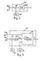
- interchange power control circuit 41 A specific example of the construction of interchange power control circuit 41 is shown in Fig. 12.
- the deviation between the active detected power value P d found by active power detector 22 and the interchange reference power value P dp set by interchange power setting device 31 is found by adder 412, amplified by interchange power regulator (APR) 411, and the D. C. current reference value I dp for controlling the interchange power is thereby formed.
- APR interchange power regulator
- the calculation P dp /E dp consisting of dividing the interchange power reference value P dp as set by interchange power setting device 31 by the D. C. voltage reference value E dp as set by D. C. voltage setting device 32 is performed by divider 413.
- the D C. current reference value I dp is created by adding the output signal of divider 413 to the output signal of interchange power regulator 411, using adder 414.
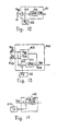
- FIG. 14 A specific example of the construction of the D. C. current control circuit 42 is shown in Fig. 14. As can be there seen, in the control circuit 42, the deviation between the D. C. current detected value I p found by the D. C. current detector 21A and the D. C. current reference value I dp produced by the interchange power control circuit 41 is determined by adder 422. This deviation is amplified by D. C. current regulator (ACR) 421, and its output signal is fed to phase control circuit 43A.
- ACR D. C. current regulator
- Phase control circuit 43A controls the firing timing of converter 5A by means of pulse amplification circuit 44A, as already described, by determining the control delay angle of externally commutated converter 5A in accordance with the output signal of D. C. current control circuit 42.
- the margin angle control system controls the firing timing of converter 5B by means of pulse amplification circuit 44B, by determining control advance angle ⁇ from a margin angle control circuit (A ⁇ C) 45 and phase control circuit 43B, such as to maintain a margin angle, in order to avoid failure of commutation of externally commutated converter 5B that carries out the D. C. to a A. C. conversion action.
- a ⁇ C margin angle control circuit
- the construction of margin angle control circuit 45 itself may be, for example, as described in published Japanese Patent Publication No. 46956/1983, so a detailed description is omitted here.
- the D. C. voltage of the power converter device is determined with a margin angle being maintained at externally commutated converter 5B, and stable operation of the power converter device is continued by controlling the D. C. current at externally commutated converter 5A for interchange power control.
- This method of control is disclosed in, for example, Japanese Patent Application laid-open No. 107443/1975.
- a first object of this inventioin is to provide a new and improved power converter device that effects interchange of power between A. C. systems and wherein both control of the interchange power and control of the reactive power can be achieved.
- a second object of this invention is to provide a novel power converter device that can easily be expanded to a multi-terminal system by the provision of additional equipment at the D. C. transmission system power converter, conventionally constructed by an externally commutated power converter.
- a voltage type self-commutated power converter 6 whose pulse width can be controlled.
- This voltage type self-commutated power converter 6 is constructed, for example, as shown in Fig. 2 by connecting six GTO elements (gate turn-off thyristor elements) 6GU, 6GV, 6GW, 6GX, 6GY, and 6GZ in a three-phase bridge arrangement. Each of these GTO elements is connected in parallel with a respective diode 6DU, 6DV, 6DW, 6DX, 6DY, and 6DZ connected in inverse polarity.
- a capacitor 6C is connected in parallel with this whole arrangement on the D. C. side.
- Externally commutated power converter 5A that performs the A/ C. to D. C. converter action is provided with a D. C. voltage control circuit 46.
- D. C. voltage control circuit 46 may be constructed for example as shown in Fig. 3.
- the deviation between the D. C. voltage reference value set by the D. C. voltage setting device 32 and the D. C. voltage detected value E d detected by D. C. voltage detector 24 is obtained by adder 461, and a control signal such as to make this deviation zero is output by D. C. voltage regulator (AVR) 462.
- AVR D. C. voltage regulator
- Externally commutated power converter 5A is controlled by the output signal of this D. C. voltage regulator 462 by means of phase control circuit 43A and pulse amplification circuit 44A.
- Interchange power control circuit 51 calculates a phase difference angle ⁇ from interchange power detected value P d , interchange power reference value P dp , reactive power reference value Q dp of voltage type self-commutated power converter 6, and A. C. voltage detected value V sd of A. C. system 1B.
- Interchange power detected value P d is detected by active power detector 22.
- Interchange power reference value P dp is set by interchange power setting device 31.
- Reactive power reference value Q dp is set by reactive power setting device 33.
- Reactive power control circuit 52 calculates a control factor M from reactive power detected value Q d of voltage type self-commutated power converter 6, reactive power reference value Q dp , D. C. voltage detected value E d , and A. C. voltage detected value V sd .
- Reactive power detected value Q d is detected by reactive power detector 23.
- D. C. voltage detected value E d is detected by D. C. voltage detector 24.
- Pulse width phase control circuit 53 generates a gate timing signal for pulse width control based on the phase difference angle found by interchange power control circuit 51 and control factor M found by reactive power control circuit 52.
- An example of this gate timing signal is shown in Fig. 7.
- Voltage type self-commutated power converter 6 is controlled by the gate timing signal that is output from pulse width phase control circuit 53 by means of on-off pulse amplification circuit 54 so as to output a voltage of the waveform shown in Fig. 7.
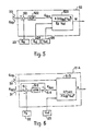
- FIG. 4 A specific example of the construction of interchange power control circuit 51 is shown in Fig. 4 and a specific example of the construction of reactive power control circuit 52 is shown in Fig. 5.
- interchange power control circuit 51 As shown in Fig. 4, the deviation between the interchange reference power value P dp set by interchange power setting device 31 and the active detected power value P d found by active power detector 22 is obtained by adder 511.
- Interchange power regulator 512 outputs an interchange power control signal P dpc such as to make this deviation zero.
- This interchange power control signal P dpc , the reactive power reference value Q dp set by reactive power setting device 33, and the A. C. voltage V sd detected by A. C. voltage detector 25 are fed to phase difference angle calculating circuit 513.
- a reactive power control signal Q dpc is obtained, as shown in Fig. 5, from the deviation between the reactive power reference value Q dp set by reactive power setting device 33 and the reactive power detected value Q d detected by reactive power detector 23, through reactive power regulator 522.
- Reactive power control signal Q dpc , D. C. voltage E d detected by D. C. voltage detector 24, and A. C. voltage V sd detected by A. C. voltage detector 25 are fed to control factor calculating circuit 523.
- Phase difference angle ⁇ is found by interchange power control circuit 51 by carrying out the calculation of equation (1).
- Control factor M is found by reactive power control circuit 52 by carrying out the calculation of equation (2).
- Phase difference calculating circuit 513 of interchange power control circuit 51 calculates phase difference angle ⁇ and control is performed such that voltage type self-commutated power converter 6 generates interchange power P dpc whilst reactive power is being generated.
- the interchange power P dpc is the output of interchange power regulator 512, so by means of the action of this interchange power regulator 512, operation is carried out with the phase difference angle ⁇ controlled such that the interchange power of voltage type self-commutated power converter 6 tracks interchange power reference value P dp .
- control factor M corresponds to the output voltage of voltage type self-commutated power converter 6.
- Reactive power control circuit 52 controls the output voltage of voltage type self-commutated power converter 6, i.e., the control factor M, so that operation is performed with its reactive power tracking the reactive power reference value Q dp .
- the phase difference angle ⁇ was calculated by equation (1), but when the value of the phase difference angle ⁇ is small, in general mathematically the following equation (10) holds, so calculation can be carried out using this equation (10).
- ⁇ X . P dpc / ( X . Q dp + V sd 2 ) (10)
- the reactive power reference value Q dp was used to find the phase difference angle ⁇ , clearly the calculation could be performed using the output of reactive power regulator 522, i.e., signal Q dpc .
Landscapes
- Engineering & Computer Science (AREA)
- Power Engineering (AREA)
- Control Of Electrical Variables (AREA)
- Supply And Distribution Of Alternating Current (AREA)
Applications Claiming Priority (2)
| Application Number | Priority Date | Filing Date | Title |
|---|---|---|---|
| JP62031061A JP2507387B2 (ja) | 1987-02-13 | 1987-02-13 | 電力変換装置 |
| JP31061/87 | 1987-02-13 |
Publications (3)
| Publication Number | Publication Date |
|---|---|
| EP0278491A2 true EP0278491A2 (de) | 1988-08-17 |
| EP0278491A3 EP0278491A3 (en) | 1989-05-24 |
| EP0278491B1 EP0278491B1 (de) | 1992-05-06 |
Family
ID=12320957
Family Applications (1)
| Application Number | Title | Priority Date | Filing Date |
|---|---|---|---|
| EP88101949A Expired EP0278491B1 (de) | 1987-02-13 | 1988-02-10 | Leistungskonverter |
Country Status (6)
| Country | Link |
|---|---|
| US (1) | US4797799A (de) |
| EP (1) | EP0278491B1 (de) |
| JP (1) | JP2507387B2 (de) |
| CN (1) | CN1004597B (de) |
| CA (1) | CA1304779C (de) |
| DE (1) | DE3870641D1 (de) |
Cited By (3)
| Publication number | Priority date | Publication date | Assignee | Title |
|---|---|---|---|---|
| WO1998016992A1 (en) * | 1996-10-14 | 1998-04-23 | Abb Power Systems Ab | Adjustable three-phase transformer |
| EP0863452A1 (de) * | 1997-03-07 | 1998-09-09 | Cegelec Controls Ltd. | Stromversorgungseinheit |
| US6437995B2 (en) | 2000-02-18 | 2002-08-20 | Alstom | Control system adapted to control operation of an ac/dc converter |
Families Citing this family (7)
| Publication number | Priority date | Publication date | Assignee | Title |
|---|---|---|---|---|
| CA1313219C (en) * | 1988-10-07 | 1993-01-26 | Boon-Teck Ooi | Pulse width modulation high voltage direct current transmission system and converter |
| JPH04190633A (ja) * | 1990-11-21 | 1992-07-09 | Hitachi Ltd | インバータの並列運転方法および並列運転インバータ装置 |
| JP3265398B2 (ja) * | 1992-01-30 | 2002-03-11 | 株式会社日立製作所 | 直流送電装置の制御装置 |
| SE514920C2 (sv) * | 1997-03-24 | 2001-05-14 | Abb Ab | Elkraftanläggning med lik- och växelspänningsnät innefattande detektering av obalanstillstånd hos strömriktare |
| JPH11135871A (ja) * | 1997-10-28 | 1999-05-21 | Nec Corp | レーザダイオード駆動方法および回路 |
| JP3547355B2 (ja) * | 1999-12-28 | 2004-07-28 | 株式会社日立製作所 | 電力変換システム |
| CN102067406B (zh) * | 2008-06-17 | 2013-07-31 | 西门子公司 | 具有自换向变流器的高压直流输电设备的调节方法 |
Family Cites Families (15)
| Publication number | Priority date | Publication date | Assignee | Title |
|---|---|---|---|---|
| JPS5527534B2 (de) * | 1973-03-12 | 1980-07-21 | ||
| JPS5385350A (en) * | 1977-01-05 | 1978-07-27 | Hitachi Ltd | Control system for multi-terminal dc transmission system |
| JPS6040254B2 (ja) * | 1978-06-14 | 1985-09-10 | 株式会社日立製作所 | 無効電力制御装置 |
| JPS5931286B2 (ja) * | 1978-10-11 | 1984-08-01 | 関西電力株式会社 | 系統連系方法 |
| EP0075319B1 (de) * | 1981-09-22 | 1985-12-18 | Matsumura, Susumu | Regelgerät für ein Gleichstrom-Energieübertragungssystem |
| JPS58112423A (ja) * | 1981-12-26 | 1983-07-04 | 株式会社東芝 | 電力変換設備の制御方式 |
| JPS58148625A (ja) * | 1982-02-26 | 1983-09-03 | 株式会社東芝 | 変換器の制御装置 |
| JPS605781A (ja) * | 1983-06-21 | 1985-01-12 | Toshiba Corp | 変換器の制御装置 |
| DE3326947A1 (de) * | 1983-07-22 | 1985-02-07 | Licentia Patent-Verwaltungs-Gmbh, 6000 Frankfurt | Verfahren und schaltungsanordnung zum betrieb einer hochspannungs-gleichstrom-verbindung zwischen zwei wechselspannungsnetzen |
| JPS60207461A (ja) * | 1984-03-29 | 1985-10-19 | Toshiba Corp | 変換装置の制御装置 |
| JPS60249824A (ja) * | 1984-05-24 | 1985-12-10 | 株式会社東芝 | 交直変換装置の制御方法 |
| JPS6112457A (ja) * | 1984-06-26 | 1986-01-20 | Toyota Motor Corp | シフトレバ−ロツク装置 |
| JPS61269377A (ja) * | 1985-05-24 | 1986-11-28 | Hitachi Ltd | 半導体装置 |
| JPS61285027A (ja) * | 1985-06-10 | 1986-12-15 | 株式会社東芝 | 交直変換装置の運転方法 |
| JPS6252617A (ja) * | 1985-08-30 | 1987-03-07 | Toshiba Corp | 調相設備の制御装置 |
-
1987
- 1987-02-13 JP JP62031061A patent/JP2507387B2/ja not_active Expired - Lifetime
-
1988
- 1988-02-10 EP EP88101949A patent/EP0278491B1/de not_active Expired
- 1988-02-10 US US07/154,312 patent/US4797799A/en not_active Expired - Fee Related
- 1988-02-10 DE DE8888101949T patent/DE3870641D1/de not_active Expired - Lifetime
- 1988-02-12 CN CN88100909.1A patent/CN1004597B/zh not_active Expired
- 1988-02-12 CA CA000558854A patent/CA1304779C/en not_active Expired - Lifetime
Cited By (4)
| Publication number | Priority date | Publication date | Assignee | Title |
|---|---|---|---|---|
| WO1998016992A1 (en) * | 1996-10-14 | 1998-04-23 | Abb Power Systems Ab | Adjustable three-phase transformer |
| EP0863452A1 (de) * | 1997-03-07 | 1998-09-09 | Cegelec Controls Ltd. | Stromversorgungseinheit |
| AU725804B2 (en) * | 1997-03-07 | 2000-10-19 | Converteam Ltd | Power supply circuits |
| US6437995B2 (en) | 2000-02-18 | 2002-08-20 | Alstom | Control system adapted to control operation of an ac/dc converter |
Also Published As
| Publication number | Publication date |
|---|---|
| CN88100909A (zh) | 1988-08-24 |
| EP0278491A3 (en) | 1989-05-24 |
| JP2507387B2 (ja) | 1996-06-12 |
| EP0278491B1 (de) | 1992-05-06 |
| DE3870641D1 (de) | 1992-06-11 |
| JPS63202229A (ja) | 1988-08-22 |
| CA1304779C (en) | 1992-07-07 |
| US4797799A (en) | 1989-01-10 |
| CN1004597B (zh) | 1989-06-21 |
Similar Documents
| Publication | Publication Date | Title |
|---|---|---|
| JP3265398B2 (ja) | 直流送電装置の制御装置 | |
| US4823251A (en) | Controller for instantaneous output current and/or voltage of 3-phase converter | |
| EP0013615B1 (de) | Steuergerät für einen Wechselstrommotor | |
| JP3102499B2 (ja) | 中性点クランプ式電力変換器の制御装置 | |
| JPS61236391A (ja) | 負荷転流式インバ−タ回路を用いた誘導電動機駆動装置 | |
| EP0278491B1 (de) | Leistungskonverter | |
| US5317500A (en) | Active no-break power transfer control for a VSCF power generating system | |
| GB2421090A (en) | Voltage source inverter control method | |
| JPS62213520A (ja) | 系統連系用電力変換装置 | |
| KR100294061B1 (ko) | 메인 인버터를 통해 전송될 전력을 제어하는 방법 | |
| US4156275A (en) | Power conversion unit | |
| US4074348A (en) | Circuit arrangement with a number of cycloconverters, particularly direct cycloconverters in y-connection | |
| JP3296065B2 (ja) | Pwmコンバータの制御回路 | |
| SE517777C2 (sv) | Anordning och förfarande för spänningsreglering i ett elektriskt transmissionsnät | |
| JP3229898B2 (ja) | 電圧形インバータ装置 | |
| JPH0553668A (ja) | 無効電力補償装置 | |
| JPS6362985B2 (de) | ||
| JP3261952B2 (ja) | Pwmコンバータ制御装置 | |
| US5717583A (en) | Power converter control apparatus for controlling commutation of switching devices under transient conditions | |
| JPH0221220B2 (de) | ||
| JPH06261584A (ja) | 交流電動機の制御装置 | |
| SU1415372A1 (ru) | Способ управлени трехфазным преобразователем частоты с непосредственной св зью | |
| JP3299718B2 (ja) | 自励式半導体電力変換装置 | |
| JP2645012B2 (ja) | 電動機制御装置 | |
| RU2031511C1 (ru) | Компенсатор реактивной мощности |
Legal Events
| Date | Code | Title | Description |
|---|---|---|---|
| PUAI | Public reference made under article 153(3) epc to a published international application that has entered the european phase |
Free format text: ORIGINAL CODE: 0009012 |
|
| AK | Designated contracting states |
Kind code of ref document: A2 Designated state(s): CH DE LI SE |
|
| PUAL | Search report despatched |
Free format text: ORIGINAL CODE: 0009013 |
|
| AK | Designated contracting states |
Kind code of ref document: A3 Designated state(s): CH DE LI SE |
|
| 17P | Request for examination filed |
Effective date: 19890607 |
|
| 17Q | First examination report despatched |
Effective date: 19910322 |
|
| GRAA | (expected) grant |
Free format text: ORIGINAL CODE: 0009210 |
|
| AK | Designated contracting states |
Kind code of ref document: B1 Designated state(s): CH DE LI SE |
|
| REF | Corresponds to: |
Ref document number: 3870641 Country of ref document: DE Date of ref document: 19920611 |
|
| PLBE | No opposition filed within time limit |
Free format text: ORIGINAL CODE: 0009261 |
|
| STAA | Information on the status of an ep patent application or granted ep patent |
Free format text: STATUS: NO OPPOSITION FILED WITHIN TIME LIMIT |
|
| 26N | No opposition filed | ||
| EAL | Se: european patent in force in sweden |
Ref document number: 88101949.1 |
|
| PGFP | Annual fee paid to national office [announced via postgrant information from national office to epo] |
Ref country code: CH Payment date: 19960308 Year of fee payment: 9 |
|
| PG25 | Lapsed in a contracting state [announced via postgrant information from national office to epo] |
Ref country code: LI Effective date: 19970228 Ref country code: CH Effective date: 19970228 |
|
| REG | Reference to a national code |
Ref country code: CH Ref legal event code: PL |
|
| PGFP | Annual fee paid to national office [announced via postgrant information from national office to epo] |
Ref country code: DE Payment date: 19991231 Year of fee payment: 13 |
|
| PGFP | Annual fee paid to national office [announced via postgrant information from national office to epo] |
Ref country code: SE Payment date: 20000207 Year of fee payment: 13 |
|
| PG25 | Lapsed in a contracting state [announced via postgrant information from national office to epo] |
Ref country code: SE Free format text: LAPSE BECAUSE OF NON-PAYMENT OF DUE FEES Effective date: 20010211 |
|
| EUG | Se: european patent has lapsed |
Ref document number: 88101949.1 |
|
| PG25 | Lapsed in a contracting state [announced via postgrant information from national office to epo] |
Ref country code: DE Free format text: LAPSE BECAUSE OF NON-PAYMENT OF DUE FEES Effective date: 20011201 |