EP0279230A2 - Video-Schnittstelle mit Datenfluss - Google Patents
Video-Schnittstelle mit Datenfluss Download PDFInfo
- Publication number
- EP0279230A2 EP0279230A2 EP88101083A EP88101083A EP0279230A2 EP 0279230 A2 EP0279230 A2 EP 0279230A2 EP 88101083 A EP88101083 A EP 88101083A EP 88101083 A EP88101083 A EP 88101083A EP 0279230 A2 EP0279230 A2 EP 0279230A2
- Authority
- EP
- European Patent Office
- Prior art keywords
- data
- pixel
- frame buffer
- bit
- output
- Prior art date
- Legal status (The legal status is an assumption and is not a legal conclusion. Google has not performed a legal analysis and makes no representation as to the accuracy of the status listed.)
- Granted
Links
- 239000000872 buffer Substances 0.000 claims abstract description 124
- 238000003860 storage Methods 0.000 claims abstract description 42
- 238000000034 method Methods 0.000 claims description 7
- 238000012545 processing Methods 0.000 claims description 7
- 230000008569 process Effects 0.000 claims description 5
- 210000001520 comb Anatomy 0.000 claims description 3
- 230000007246 mechanism Effects 0.000 claims description 3
- 230000006870 function Effects 0.000 abstract description 24
- 230000008707 rearrangement Effects 0.000 abstract description 7
- 239000003086 colorant Substances 0.000 abstract description 6
- 238000004364 calculation method Methods 0.000 abstract description 3
- 238000004891 communication Methods 0.000 abstract description 2
- 238000011065 in-situ storage Methods 0.000 abstract 1
- 101100018928 Drosophila melanogaster InR gene Proteins 0.000 description 15
- 238000010586 diagram Methods 0.000 description 8
- 238000013459 approach Methods 0.000 description 6
- 238000012546 transfer Methods 0.000 description 3
- 239000013598 vector Substances 0.000 description 3
- 230000002457 bidirectional effect Effects 0.000 description 2
- 238000013461 design Methods 0.000 description 2
- 230000000873 masking effect Effects 0.000 description 2
- 230000003252 repetitive effect Effects 0.000 description 2
- 238000011160 research Methods 0.000 description 2
- 101100464782 Saccharomyces cerevisiae (strain ATCC 204508 / S288c) CMP2 gene Proteins 0.000 description 1
- 101100464779 Saccharomyces cerevisiae (strain ATCC 204508 / S288c) CNA1 gene Proteins 0.000 description 1
- 230000009471 action Effects 0.000 description 1
- 230000009286 beneficial effect Effects 0.000 description 1
- 230000008901 benefit Effects 0.000 description 1
- 238000006243 chemical reaction Methods 0.000 description 1
- 230000006378 damage Effects 0.000 description 1
- 238000013500 data storage Methods 0.000 description 1
- 230000001419 dependent effect Effects 0.000 description 1
- 238000001514 detection method Methods 0.000 description 1
- 238000010348 incorporation Methods 0.000 description 1
- 230000003993 interaction Effects 0.000 description 1
- 230000002452 interceptive effect Effects 0.000 description 1
- 238000013507 mapping Methods 0.000 description 1
- 201000003034 pontocerebellar hypoplasia type 4 Diseases 0.000 description 1
- 230000002829 reductive effect Effects 0.000 description 1
- 230000002441 reversible effect Effects 0.000 description 1
- 230000003068 static effect Effects 0.000 description 1
- 239000002699 waste material Substances 0.000 description 1
Images


Classifications
-
- G—PHYSICS
- G09—EDUCATION; CRYPTOGRAPHY; DISPLAY; ADVERTISING; SEALS
- G09G—ARRANGEMENTS OR CIRCUITS FOR CONTROL OF INDICATING DEVICES USING STATIC MEANS TO PRESENT VARIABLE INFORMATION
- G09G5/00—Control arrangements or circuits for visual indicators common to cathode-ray tube indicators and other visual indicators
- G09G5/36—Control arrangements or circuits for visual indicators common to cathode-ray tube indicators and other visual indicators characterised by the display of a graphic pattern, e.g. using an all-points-addressable [APA] memory
- G09G5/39—Control of the bit-mapped memory
- G09G5/393—Arrangements for updating the contents of the bit-mapped memory
Definitions
- the present invention relates to video adapters with improved data pathing, generally in the field of interfacing between a computer and an attached raster scan video display monitor and is thought to provide, in a small inexpensive stand alone workstation, many functions previously unavailable to small micro and mini systems.
- the present invention describes functions that can be incorporated into a video display adapter to provide, in stand alone workstations, the graphic functions and performance required by such complex graphic applications.
- Such increased capability display adapters are especially needed for such small stand alone systems as the IBM PC/AT and the IBM RT-PC which can provide high-performance, moderate-cost adapter functions which cover a very broad spectrum of applications.
- the principle role of the pixel data path is to provide a host processor with a convenient access to frame buffer data.
- the frame buffer architecture usually supports either the pixel or plane structure of an image. It means that the conventional architecture provides good performance only for a particular area of application.
- a processor word can stand for four (8 bit) pixels for pixel-oriented applications, or for 32 bits of the same plane for plane-oriented problems or for a corresponding number of pixel "slices" for processing pixel data fields.
- the host data bus is "hard-wired" to a frame buffer, the host must rearrange words, placing bits in relation to the frame buffer I/O layout.
- bit-blt primitive J. D. Foley, A. Van Dam, "FUNDAMENTALS OF INTERACTIVE COMPUTER GRAPHICS", Addison-Wesley, Reading, MA. 1982, pp. 465, 484-485, allows increased performance only for simple area copy or logical operations between planes.
- the incorporation of arithmetic operations into the bit-blt hardware has been tried but has generally proved useless for colour graphics, so the processing of colours has been usually done by the host.
- An all-point addressable frame buffer (such as described in EP-A- , (YO9-86-105) requires a certain kind of data alignment, which is able to provide a proper order of bits in the accessed word independently of its address, Robert F. Sproull, Ivan E. Sutherland, Alistair Thompson, Satish Gupta, and Charles Minter, "THE 8 BY 8 DISPLAY", ACM Trans. Graphics, Vol. 2, No. 1, Jan. 1983, pp. 32-56.
- the host processor may handle such an operation but in the time-consuming and application dependent manner.
- the present invention provides a special alignment unit which makes this alignment invisible for the user.
- the performance for plane-oriented operations may be reduced drastically due to the narrower frame buffer data width.
- the data path may be 4 times wider than is the case with 1 Meg chips (256K by 4).
- the patents describe a frame buffer which can be accessed conveniently only by planes. In order to access a pixel, all planes must be read in parallel.
- an external device e.g., a microprocessor
- the present invention provides a simple rearrangement of the frame buffer data path, modifying it in a way which is convenient both for arithmetic operations on pixel values as well as logical operations on bit values.
- an additional rearrangement of the input/output interface is done. It provides a convenient interface with an external microprocessor, based on an application's requirements. It means, that from the point of view of the microprocessor, the frame buffer it may be made to look like it is organised plane-wise, or pixel-wise or slice-wise. In cases where the frame buffer is being used for an application where the pixel or slice access is more important, than the bit-wise access, it provides much higher performance by reducing the external processor's overhead.
- the present invention provides a video adaptor for connecting a raster display type monitor to a host computer system including an I/O serving data bus, a digital signal processor, a pixel processor and a frame buffer for storing video data to be displayed on the monitor, the frame buffer having all-point-addressable access to M pixels, each having Z-bits of video data, of a row of pixels on the monitor screen which may not be word aligned, in a single memory cycle, the adapter including, in the pixel processor architecture, input means for converting video data in a pixel, pixel slice or plane mode format on the host data bus to a uniform internal format, means for automatically aligning and storing locally, data to be stored in or accessed from the frame buffer which is not aligned along physical word boundaries, means for selectively performing logical or arithmetic operations on video data stored in the pixel processor, and means for reformatting data processed by the pixel processor into a format suitable for presentation to the host system.
- the present invention also provides a video adaptor for connecting a raster display type monitor to a host computer system including an I/O bus, a digital signal processor, a pixel processor and a frame buffer for storing video data to be displayed on the monitor, the frame buffer having simultaneous all-point-addressable access to M pixels, each having Z bits of video data, of a row of pixels on the monitor screen which may not be word aligned, in a single memory cycle, including input interface means for converting data on the host data bus from possible data formats including pixel, pixel slice and plane to a standard internal configuration wherein pixels are stored and may be operated on in a fixed predetermined internal format, the input means further including means for converting data received on the host data bus having a first narrow bandwidth, to a format in which it may be processed internally and transferred to the frame buffer, in a format having a substantially wider bandwidth, means for automatically aligning and temporarily storing, data to be stored in or accessed from the frame buffer which is not aligned along physical word boundaries, the means for aligning
- the present invention further provides an adapter for interfacing between a host processor and the local frame buffer memory of a raster scan display monitor and including a pixel processor, the pixel processor being adapted to selectively process video data accessed from the frame buffer and/or from the host processor, the frame buffer having the capability of accessing a row of M pixels each having Z bits of video data accessible on an all-point-addressable basis starting at any pixel address on the screen, the pixel processor including; an input interface unit for converting video data received from the host in pixel, pixel slice, or plane format on a narrow bandwidth data bus into a uniform internal format for presentation to the frame buffer and to the logic and storage circuitry in the pixel processor, Z plane channel units for storing and aligning at least M bits of video data the data being selectively received from the input interface unit, the frame buffer, or one or more of M arithmetic/logic units in the pixel processor, the M arithmetic/logic units being actuable to selectively perform both logic and arithmetic operations on
- the video display adapter is envisioned as a high resolution, medium function graphics display adapter which could drive any of a number of currently available display monitor units such as the IBM 5081. In a currently realisable form, it will support such a monitor with a resolution of 1024 by 1024 pixels and provides eight bits per pixel of video data information which provides 256 possible control features which may be distributed between colour and/or gray scale data.
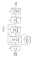
- the overall adapter consists of the following major components.
- the digital signal processor 10 is utilised to manage the overall adapter's resources and it transforms display coordinates and performs a number of other fairly sophisticated signal processing tasks.
- the instruction and data storage block 12 is an instruction RAM which can be loaded with additional micro code for the signal processor as will be understood.
- Block 12 also acts as a data RAM and provides the primary interface between signal processor 10 and the system processor. It also performs the function of being a main store for the signal processor 10.
- Block 14 labled command FIFO, serves as an input buffer for passing sequential commands to the digital signal processor 10 via I/O bus 16 and, as is apparent, connects the video display adapter to the system processor.
- the pixel processor 18 contains logic that performs a number of display supporting functions such as line drawing and address manipulation which permits finite areas of the display screen to be manipulated (bit-blt).
- a number of the novel aspects of the present display adapter are resident in the pixel processor block.
- Block 20 comprises the video random access memory which feeds the monitor through appropriate digital/analog conversion circuitry.
- the configuration herein disclosed has a resolution of approximately 1K by 1K pixels wherein each pixel represents a discrete element of video data to be displayed on the monitor.
- Each pixel may contain as much information as is storable in the eight planes of the frame buffer which, is as well understood, means that there are eight bits of data per pixel. As will further be understood, these eight bits may be distributed among the red, green and blue of a colour monitor or simply for intensity information in a gray scale black and white monitor.
- the improvements thought to be provided by the present invention are in the architecture of the pixel processor 18 and provide a number of features which permit the operation of the video adapter to be significantly speeded up as will be apparent from the subsequent description.
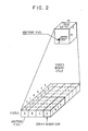
- the 8-bit frame buffer with the resolution 1K by 1K has a four-in-line (pixel) all-point addressable access.
- Such a frame buffer could be constructed of eight 256K by 4 memory chips, as shown in FIG. 2.
- the frame buffer I/O data is 32 bit in width and provides read/write operation for 4 pixels in parallel, although it will be readily appreciated that a greater or lesser number of pixels could be provided.
- frame buffer architecture disclosed and described in EP-A- , (YO9-86-105) would also provide 4 pixels in parallel. It has the extra capability of providing very fast access to an additional three rows of 4 pixels for a total of 4 by 4 or a sixteen pixel square array. Of course, the number of pixels in a row access could be readily changed by changing the number of memory chips and the number of shift register accumulators and appropriate control circuitry as will be readily understood.
- the host data bus width is 16 bits. All results can be easily, and in the same manner, extended to a frame buffer built with lower density chips and/or a square access configuration (as mentioned above) and for a different host data bus width.
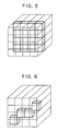
- the 16 bit host processor word can be interpreted differently, depending on application.
- two pixels (FIG. 3), four 4-bit pixel slices (FIG. 4) or 16 bits of the same plane of a 4 by 4 pixel array (FIG. 5) can be updated or read.
- a 4-bit vector can be written into the frame buffer (FIG. 6) using a masking mechanism.
- masking is considered as a part of the frame buffer write enable control as described in EP-A- , ( YO9-86-105) and is not considered to be a part of the present data path hardware.
- the host processor 16-bit data word would have a different layout or organisation for plane, pixel and slice modes (FIG. 7). Two left or two right pixels (of a 4 pixel access) in the pixel mode and lower halves or upper halves of all four pixels in the slice mode can be processed.
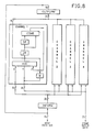
- the data path architecture may be represented, in the simplest case, as consisting of four channels, each one serving one pixel (FIG. 8).
- the pixel channel includes a multiplexor MUX, destination register DR, source register SR, a combination unit COMB and a tri-state buffer B.
- the 3-to-1 multiplexor MUX allows the DR register to accept either frame buffer data, or host data, or the result of the SR and DR data combination from the COMB unit.
- the DR and SR registers serve bit-blt operations, storing frame buffer source and destination data.
- the COMB unit provides logic and arithmetic operations on the DR and SR data.
- the output of the MUX is also connected to the buffer B, supplying update data to the frame buffer I/O bus.
- the registers SR and DR are pipelined, allowing a number of different bit-blt operations. For example, combination bit-blt can be done for four pixels in parallel and repeatedly for a larger pixel area (e.g., 4 ⁇ 4).
- host data may be transferred into the SR register, and be used as constant source data for clearing a desired area of the frame buffer or as a constant source for copy or combination bit-blt. In the latter case, the SR update must be disabled after the host data is loaded into it.
- INFORM the In-Data Formatter
- OUTFORM Out-Data Formatter
- Each channel of the data path on FIG. 8 has an 8-bit structure, which makes it inconvenient to work with plane-oriented applications but makes it possible to provide a COMB unit with pixel data for pixel-oriented applications.
- the communication between the frame buffer and pixel data path is preferably implemented not in 'pixel-wise', but in a combination 'pixel-plane-wise' manner (FIG. 9).
- the data path consists of eight 4-bit plane channels PLH 0-7 and four 8-bit combination units COMB (0-3).
- the 4-bit planes 0-7 of the frame buffer, shown in FIG. 2 are connected to corresponding Y inputs of the 4-bit multiplexors, MUX of the plane channels PL H0-7 as shown in FIG. 10.
- the four bit registers SR and DR of each of the plane channels (PCH) have the same connections with each other and multiplexors MUX as was shown in FIG. 8. But the outputs of the plane channels' DR and SR registers are connected to the four 8-bit combination units COMB in such a way that each of the units is provided with the required pixel data. Accordingly, three internal 32-bit data buses are shown in FIG. 9.
- the destination bus accepts all outputs of the DR registers
- the source bus is connected to the outputs of the SR registers
- the combination bus accepts outputs of the COMB units.
- the SR registers in the lower four channels PCH O-3 are loaded by LD1 signal and the SR registers in the upper four channels PCH4-7 are loaded by LD2 signal.
- the COMB 0 A-input takes the eight bits 0 of all of the DR registers
- the B-input of the COMB 0 is connected to bits 0 of all of the SR registers
- the A-input of the COMB 1 is connected to bits 1 of all of the DR registers, etc.
- the A inputs of COMB 0 take pixel 0 data from the destination bus.
- the B inputs of COMB 0 take pixel 0 data from the source bus, etc.
- COMB 0 A ⁇ 0 > input takes bit 0 of pixel 0 from destination bus
- COMB 0 B ⁇ 0 > input takes bit 0 of pixel 0 from the source bus, etc.
- the 8-bit COMB outputs are distributed to the corresponding Z inputs of the multiplexors MUX (as shown in FIGS. 9 and 10), in a way that each PCH gets the correct 4-bit plane data.
- the eight bits 0 of the Z inputs of the MUX multiplexors in PCH 0-7 are connected to bits 0-7 of the COMB 0 unit, bits 1 of Z inputs are connected to bits 0-7 of the COMB 1 unit, etc.
- the COMB units may provide arithmetic or logical operations on pixels in parallel.
- logical operations on the corresponding pixel bits deliver the required logical combination operations on planes.
- BSH 4-bit barrel shifters
- FBWE frame buffer write enable signal
- the BSH location is chosen to be between the MUX and DR register which allows it to be used twice during read (FBWE signal is disabled) and write operations (FBWE signal is enabled), insuring that the frame buffer data alignment is done automatically without any host intervention.
- the input bits of the MUX are referred to as A,B,C,D for each 4-bit path X,Y,Z which connects the corresponding MUX output bits A,B,C,D to the bits 0-3 of the register DR (FIG. 10).
- the shift number to the barrel shifter BSH is zero, and the bits A of all Y-inputs of the multiplexors MUX will be connected to the left most pixel A (the least significant bit 0 of the pixel A will be connected to the bit A of the input Y of the MUX in the PCH 0, the most significant bit 7 of the pixel A will be connected to the bit A of the MUX in the PCH 7), the bits B of all Y inputs will be connected to the next pixel B, etc.
- pixel A data bits 0..7 are connected to the bits 0 of register DR in the channels PCH 0..7
- pixel B data bits 0..7 are connected to the bits 1 of registers DR in the channels PCH 0..7, etc.
- the pixels A,B,C and D data that is read from the frame buffer feeds the bits B,C,D,A of the multiplexors Y inputs.
- the barrel shifters shift the MUX outputs one position in the left direction, and the bits 0 of the DR registers again accept pixel A data, bits 1 accept pixel B data, etc.
- the shift will be one position to the right, providing proper distribution of pixels to the corresponding frame buffer I/O pins.
- pixel alignment is done by equally shifting the eight planes.
- FIG. 11 should be referred to for the purpose of seeing how the various bits and pixels as numbered in FIGS. 2, 7 and 12 to 14 are stored in and passed through the Data In Formatter of FIG. 11. See especially the organisation of the bits passing through the two Input Multiplexors (INMUX 1 and 2). As will be apparent to those skilled in the art ---the bit designations in the lower portion of the two INMUX units do not imply storage, but are only intended to show diagrammatically how the organisation of the bits constituting the pixels, pixel slices, or planes are organised as they pass through this unit during the three possible operating modes. This figure thus clearly indicates how the overall architecture operates on the host data by keeping track of the various pixels and planes as the data passes into the plane channel logic.
- This unit In order to update the frame buffer using host data, it should be loaded into the data-in register DINR of the INFORM unit (FIG. 11).
- This unit also includes two multiplexors INMUX1 and INMUX2, which distribute host data bits to the proper X input bits of the multiplexors MUX in the plane channels.
- Each INMUX multiplexor depending on the 'mode' will accept one of three 16-bit words and passes one of them to the 16-bit output. It consists of sixteen 3-to-1 multiplexors and is controlled by a 3-bit MODE SELECT signal. There are three modes - 'plane', 'slice' and 'pixel', that correspond to the four possible layouts of the host data word (FIG. 7).
- the outputs 0..15 of the INMUX multiplexors are connected to the X-inputs of the MUX multiplexors in a way shown in FIG. 6.
- the outputs 0..15 of the DINR are connected to the six 16-bit inputs of INMUX multiplexors in a particular order, which is also fully illustrated by FIG. 11 by the numbers typed in the INMUX bodies.
- outputs 0..3 of the INMUX1 or INMUX2 are connected only to the bit 0 of the DINR
- outputs 4..7 are connected to the bit 1 of the DINR, etc.
- outputs 0..3 are connected to the bits 0..3 of the DINR, and so on.
- bits 0..3 of the INMUX1 output are connected to the bits 0..3 of the DINR
- bits 4..7 are connected to the bits 8.11 of the DINR
- bits 0..3 of the INMUX2 output are connected to the bits 4..7 of the DINR, etc.
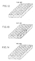
- host data (FIG. 7) is distributed to the pixels and planes as shown in FIGS. 12-14.
- 16-bit data word may be written into the frame buffer pixel locations directly or may be loaded into the DR registers, correspondingly to pairs of pixels A,B and C,D and then be used for updating any pair of pixels.
- host data word may be used for updating lower halves of all 4 pixels or upper halves of all 4 pixels.
- bits 0..3 may be loaded into any plane of the frame buffer.
- this register In order to avoid the wasting of 12 bits of the DINR when working in the 'plane' mode, this register also has a special structure. In essence, it consists of four 4-bit pipelined register's (FIG. 11).
- the host 16-bit data is loaded into the DINR register by signal LOAD making bits 0..3 ready for loading into the frame buffer.
- the tailing edge of the FBWE signal shifts DINR data four position to the left, making next four bits 4..7 ready for frame buffer updating.
- the four write cycles for example, in page mode (writing in horizontal direction) or under Bit-Blt addressing control (in vertical or diagonal direction) all 16 bits of the host data word are written in the frame buffer.
- the host has additional time to prepare the next word during those four write cycles, so the combination of host DMA mode and Frame buffer page mode may be combined. Also for such a "burst" update, an additional register may be used. It will accept the host data, transfer it to the DINR and while the DINR is used for shifting plane data, this register is free to accept the next data from the host.
- the XAD ⁇ 0,1> should be 0,0, 'disabling' the alignment hardware.
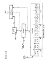
- the next requirement of the pixel data path is to prepare data that is to be read from the frame buffer for the host data bus.
- This function is implemented by Data-Out Formatter unit (OUTFORM), shown on FIG. 15. It includes pixel-slice multiplexor PXSLMUX, plane multiplexor PLMUX, a 12-bit register OUTR, and multiplexor OUTMUX.
- OUTFORM Data-Out Formatter unit
- PXSLMUX pixel-slice multiplexor
- plane multiplexor PLMUX plane multiplexor PLMUX
- OUTR 12-bit register
- multiplexor OUTMUX The 64-to-16 PXSLMUX multiplexor provides 16-bit output of the 32-bit destination bus under control of 2-bit MODE CONTROL signal.
- any pair A,B or C,D of 8-bit pixels is transferred to the inputs of the OUTMUX multiplexor providing the two left most or two right most pixels' data to the OUTMUX inputs.
- the 'slice' mode lower or upper halves of all four pixels are delivered to the OUTMUX inputs.
- the 'plane' mode also uses the PXSLMUX in the 'slice' mode, but the halves of four pixels selected by PXSLMUX are used as input data to the 16-to-4 PLMUX multiplexor, which in turn selects a particular plane (one of four planes) under control of the plane number PLN signal. If, for example, plane 5 should be read from the frame buffer, the PSPLMUX provides the upper halves of the pixel data, and the PLMUX delivers four bits of the plane 5 to the OUTMUX.
- the OUTR register serves this purpose. It consists of three pipelined 4-bit registers, and uses the frame buffer read signal FBRD as a transfer clock. In essence, the OUTR structure is the same as the INDR, but the upper register role is played by the DR. After four memory read cycles, the lower 12 bits will be stored in the OUTR, and the upper four bits will be provided by the DR registers. That 16-bit data from the same plane now is ready to be transferred to the host data bus by the OUTMUX multiplexor.
- the last function of the pixel data path is to provide assistance to the colour antialiasing copy of graphics objects. It is especially important for high performance typing of high quality text for low and medium cost displays.
- the subsequent description will refer to a text typing, although it does not depend on the object's shape.
- pixel data has two fields representing colour code and intensity code.
- the colour on the screen is based on the loading of the video look-up table and does not require any particular distribution of pixel bits between fields.
- the host processor compares the source and destination pixel intensities and colours and decides what colour and intensity codes are to be assigned to the destination.
- the idea of the present invention is to make use of the fact that 16 levels of intensity is generally sufficient for practical purposes even for high resolution displays.
- 16 levels of intensity is generally sufficient for practical purposes even for high resolution displays.
- one of each always represents the intensity and another one represents the colour codes, 15 colours of antialiasing text can be provided on any particular background colour.
- the algorithm for calculating a new destination intensity may be illustrated with the following procedure: The destination colour remains the same.
- the conventional 8-bit arithmetic-logic unit which may be incorporated in the COMB unit, should include an additional logic block which is shown on FIG. 16.
- This addition includes two 4-bit comparators CMP1 and CMP2, XNOR and AND gates, and a 4-bit multiplexor MUX.
- the output of the MUX provides a new DI value, while DC is derived directly from the input to the logic block as shown.
- the antialiasing copy operation may be described as follows.
- the host provides the data path with two 16-bit words, representing the first four source pixels colour and intensity.
- the first 16 bit word representing the source colour is transferred into the source registers SR bits 4-7 (shown in FIGS. 9 and 10) and following the loading of those registers, the next 16 bit word representing the first 4 pixels intensity values is loaded into the destruction registers DR bits 0-4.
- the host supplies only 16-bit intensity values, providing parallel update of 32 bits of four destination pixels.
- the antialiasing copy is especially important for colour displays with a small number of bits per pixel.
- the disclosed principles of building the pixel data path are applicable to a longer pixel value. But, for example, in real colour systems with 24-bits per pixel, the necessary calculations may be done directly on pixel colour values, not colour and intensity codes. See, the article by C. J. Evangelisti, L. Lumelsky and P. N. Sholtz, "COPY OPERATION FOR COLOR ANTIALIASING", IBM Technical Disclosure Bulletin, Vol. 27, No. 10B, March 1983, pp. 6234-6236.
- System Data Bus In and System Data Bus Out are connected to the host microprocessor that controls the display subsystem. It is a 16-bit bidirectional bus. Memory Data Bus In and Out are connected to the frame buffer. It is a 32-bit bidirectional bus.
- a memory "read” cycle takes data from the memory data bus, passes this data through the plane select logic, data path MUX in, data barrel shift, logic unit, and stores the data in the ACCUM latch.
- a memory "WRITE” cycle takes data from the system data bus, passes this data through the pixel/half slice data format logic, data path MUX in, data barrel shift, logic unit, and stores the data in the ACCUM latch.
- the frame buffer memory is then cycled, passing the data through both data path MUXIS, the data barrel shift, and out to memory through the memory data bus MUX.
- a memory “LOAD” cycle is very similar to a “READ” cycle, except that the system does not read data from the ACCUM latch.
- a memory “STORE” cycle takes data in the ACCUM latch and stores it into the bit map memory in the same manner as the "write” cycle, and again the system is not involved in this cycle. Each part of the data path logic is described below.
- This logic connects the 16-bit microprocessor bus to the 32 bit data path circuit.
- the memory organisation of the frame buffer is shown in FIG. 18. In this organisation, pixels are interleaved in the memory in groups of four. Because each pixel is made up of 8 bits (1 bit per plane of memory) for any memory access, 32 bits of data are controllable. In this implementation, the system is capable of writing to the frame buffer memory in one of two formats. In the "pixel" mode, data can be written to either of the outer pairs of adjacent pixels through all 8 bits.
- a write cycle will map system data bits 15 to 8 into pixel 0 bits 7 to 0 respectively, and system data bits 7 to 0 into pixel 1 bits 7 to 0 respectively.
- system data is mapped to all four pixels, either into bits 0 to 3 or 4 to 7 under control of a control bit in the static command register.
- This same logic is placed on the output side of the ACCUM latch to allow these same format modes to be used when the system reads data loaded into the accumulator from the bit map (a memory "read” cycle).
- the thirty-two bit memory data bus is arranged as four pixels of 8-bit planes per pixel.
- the data path logic shown as thirty-two bits, is implemented as 8 four-bit "plane channels". Each plane of data is operated on separately, and merged for output to the bit map memory.
- the plane select logic is provided for moving data from one selected plane of memory to the "plane channels" of the other planes. It is used, for example, when a mask is stored in one plane to allow the mask data to be logically mixed with data on all other planes.
- This circuit provides for multiple sources of data that must flow through the barrel shifter and logic unit circuitry. These sources are, 1) System Data, 2) Frame Buffer Memory Data, 3) Accumulator Data. Since these data sources must each use the barrel shifter and logic unit to allow for unaligned (not along word boundary) data accesses to the frame buffer, it is very beneficial to use this multiplexor approach to save logic over providing each path with a separate barrel shifter and logic unit. There is no performance penalty in providing this multiplexing function since only one of these paths can be active for a given memory cycle, and a new path can be specified on each memory cycle.
- the barrel shifter circuit is composed of 8 groups of 4-bit barrel shifters. Each 4-bit barrel shifter works on a plane channel. For a read cycle, the barrel shifter is used to align the data that comes from memory before passing it to the logic unit and accumulator. The system then reads the data from the accumulator and the barrel shifter is not involved. For a write cycle, the barrel shifter is set to pass unshifted system data into the logic unit and accumulator. A memory cycle is then initiated and data is passed from the accumulator through the data path multiplexors to the barrel shifter for alignment before being written to the frame buffer. For a load cycle, the barrel shifter is used to align the data that comes from memory before passing it to the logic unit and accumulator. For a store cycle, a memory cycle is initiated and data is passed from the accumulator through the data path multiplexors to the barrel shifter for alignment before being written to the frame buffer.
- the logic unit has two input paths, the first is for data coming through the barrel shifter and data path MUX in, the second is from the ACCUM latch. This allows logic operations to be per- formed on incoming data with data already stored in the accumulator latch. The logic unit is only involved in "read/write” cycles and "load” cycles, it is not involved in the "store” cycle.
- the logic unit functions include: pass barrel shift data or inverted barrel shift data, pass ACCUM. latch data or inverted ACCUM latch data. Also provided are the following functions of two variables, AND, OR, XOR, NAND, NOR, XNOR of the barrel shift data and the ACCUM latch data.
- the accumulator latch is the main latch in the system. This latch holds data coming from the system before being written to the frame buffer. It also holds data read from the frame buffer before passing it to the system. In “load and store” cycles, this latch is used to hold the data as it flows from source to destination within the frame buffer.
- This logic is designed to allow the detection of lines that are drawn over one another. This is a very useful function in design applications were the user is interacting with a drawing and adding new lines.
- the logic consists of 3 registers and a comparison circuit. One register is loaded with the compare colour, the second register is loaded with the "hit” colour, and the third register is loaded with the "miss” colour.
- a load/store cycle must be coded in the instruction queue. As a new line is drawn, data is first loaded into the accumulator and compared on a pixel by pixel basis with the compare colour, if a match is found then for that pixel the "hit" colour is written by the store cycle, for all the pixels that do not match the compare colour, the store cycle writes the "miss” colour. To make this function work, the application would load the compare colour with the colour of the lines they were looking for.
- a highlighting action will occur in this mode.
- a register is included in the circuit to enable only selected planes to be used in the comparison of colours. That is, by setting this register to certain values, different planes of memory can be selectively "don't cared" out.
- This logic selects data from the line on line circuit or data from the accumulator latch to be written out to memory.
- this logic For every memory write cycle this logic multiplexes the write per bit information and the memory data out to the frame buffer. Using the write per bit feature of the frame buffer allows for selective plane writes to be performed.
- This circuit provides a means for performing logical operations or colour expansion on "A leg" data with a constant stored in the constant register. Since the value in the ACCUM latch is destroyed during the logical op, the colour is stored in the Constant Reg and the B Leg MUX is set to pass this data to the Logic Unit.
- This circuit is designed to streamline the data path operations of a large frame buffer with several unique logic features.
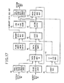
- FIG. 17 the architecture of the embodiment of FIG. 17 is somewhat different from that of the embodiment of FIGS. 8 and 10, however, the functions performed are substantially co-extensive.
- the following is a brief listing of the functionally analogous blocks between the two embodiments. The numbered blocks refer to the functional blocks of FIG. 17.
- Block 10 is equivalent to the Inform block of FIG. 8.
- Block 12 is equivalent to the Outform block of FIG. 8.
- the functions of blocks 14 and 15 are performed by the MUX of FIGS. 8 and 10.
- Block 16 is equivalent to the BSH (barrel shifter) of FIGS. 8 and 10.
- the functions of block 18, 20 and 22 are performed essentially by the COMB blocks of FIGS. 8 and 10.
- Block 24 is equivalent to the DR block of FIGS. 8 and 10.
- the function of block 26 would be performed by the SR block of FIGS. 8 and 10.
Landscapes
- Engineering & Computer Science (AREA)
- Physics & Mathematics (AREA)
- Computer Hardware Design (AREA)
- General Physics & Mathematics (AREA)
- Theoretical Computer Science (AREA)
- Image Generation (AREA)
- Digital Computer Display Output (AREA)
- Controls And Circuits For Display Device (AREA)
- Image Input (AREA)
Applications Claiming Priority (2)
| Application Number | Priority Date | Filing Date | Title |
|---|---|---|---|
| US07/013,847 US4823286A (en) | 1987-02-12 | 1987-02-12 | Pixel data path for high performance raster displays with all-point-addressable frame buffers |
| US13847 | 1998-01-27 |
Publications (3)
| Publication Number | Publication Date |
|---|---|
| EP0279230A2 true EP0279230A2 (de) | 1988-08-24 |
| EP0279230A3 EP0279230A3 (de) | 1991-07-31 |
| EP0279230B1 EP0279230B1 (de) | 1994-11-09 |
Family
ID=21762094
Family Applications (1)
| Application Number | Title | Priority Date | Filing Date |
|---|---|---|---|
| EP88101083A Expired - Lifetime EP0279230B1 (de) | 1987-02-12 | 1988-01-26 | Video-Schnittstelle mit Datenfluss |
Country Status (4)
| Country | Link |
|---|---|
| US (1) | US4823286A (de) |
| EP (1) | EP0279230B1 (de) |
| JP (1) | JPH0810464B2 (de) |
| DE (1) | DE3852045T2 (de) |
Cited By (4)
| Publication number | Priority date | Publication date | Assignee | Title |
|---|---|---|---|---|
| EP0403122A3 (de) * | 1989-06-16 | 1992-08-05 | International Business Machines Corporation | Rechnergesteuerte Bildüberlagerung |
| EP0410777A3 (en) * | 1989-07-28 | 1992-10-28 | Texas Instruments Incorporated | Video graphics display memory swizzle logic circuit and method |
| EP0617402A3 (de) * | 1989-07-28 | 1995-04-26 | Hewlett Packard Co | Verfahren und Einrichtung zur Beschleunigung von Bildfenstern in graphischen Systemen. |
| EP0885529A4 (de) * | 1996-03-07 | 1998-12-23 |
Families Citing this family (46)
| Publication number | Priority date | Publication date | Assignee | Title |
|---|---|---|---|---|
| US6336180B1 (en) | 1997-04-30 | 2002-01-01 | Canon Kabushiki Kaisha | Method, apparatus and system for managing virtual memory with virtual-physical mapping |
| US4924410A (en) * | 1986-02-13 | 1990-05-08 | Hitachi, Ltd. | Display control method and system |
| JP2550570B2 (ja) * | 1987-04-16 | 1996-11-06 | ブラザー工業株式会社 | 印字装置 |
| JPH0736162B2 (ja) * | 1988-04-18 | 1995-04-19 | 株式会社日立製作所 | 図形処理装置 |
| USRE39529E1 (en) | 1988-04-18 | 2007-03-27 | Renesas Technology Corp. | Graphic processing apparatus utilizing improved data transfer to reduce memory size |
| US4967392A (en) * | 1988-07-27 | 1990-10-30 | Alliant Computer Systems Corporation | Drawing processor for computer graphic system using a plurality of parallel processors which each handle a group of display screen scanlines |
| US5062057A (en) * | 1988-12-09 | 1991-10-29 | E-Machines Incorporated | Computer display controller with reconfigurable frame buffer memory |
| KR920002600B1 (ko) * | 1989-07-21 | 1992-03-30 | 삼성전자 주식회사 | 1비트/2비트 플레인 겸용 비디오 보드 |
| US5233690A (en) * | 1989-07-28 | 1993-08-03 | Texas Instruments Incorporated | Video graphics display memory swizzle logic and expansion circuit and method |
| US5269001A (en) * | 1989-07-28 | 1993-12-07 | Texas Instruments Incorporated | Video graphics display memory swizzle logic circuit and method |
| US5287470A (en) * | 1989-12-28 | 1994-02-15 | Texas Instruments Incorporated | Apparatus and method for coupling a multi-lead output bus to interleaved memories, which are addressable in normal and block-write modes |
| US5319395A (en) * | 1990-05-16 | 1994-06-07 | International Business Machines Corporation | Pixel depth converter for a computer video display |
| US5566283A (en) * | 1990-09-03 | 1996-10-15 | Dainippon Printing Co., Ltd. | Computer graphic image storage, conversion and generating apparatus |
| JPH06103599B2 (ja) * | 1990-11-16 | 1994-12-14 | 三菱電機株式会社 | 半導体集積回路装置 |
| US5313576A (en) * | 1990-11-23 | 1994-05-17 | Network Computing Devices, Inc. | Bit aligned data block transfer method and apparatus |
| US5345555A (en) * | 1990-11-23 | 1994-09-06 | Network Computing Devices, Inc. | Image processor memory for expediting memory operations |
| US6088045A (en) * | 1991-07-22 | 2000-07-11 | International Business Machines Corporation | High definition multimedia display |
| US5613053A (en) | 1992-01-21 | 1997-03-18 | Compaq Computer Corporation | Video graphics controller with automatic starting for line draws |
| ATE137040T1 (de) * | 1992-01-21 | 1996-05-15 | Compaq Computer Corp | Graphische videokontrolleinheit mit verbesserten rechenfaehigkeiten |
| US5687376A (en) * | 1994-12-15 | 1997-11-11 | International Business Machines Corporation | System for monitoring performance of advanced graphics driver including filter modules for passing supported commands associated with function calls and recording task execution time for graphic operation |
| US6307559B1 (en) * | 1995-07-13 | 2001-10-23 | International Business Machines Corporation | Method and apparatus for color space conversion, clipping, and scaling of an image during blitting |
| US5826054A (en) * | 1996-05-15 | 1998-10-20 | Philips Electronics North America Corporation | Compressed Instruction format for use in a VLIW processor |
| US8583895B2 (en) | 1996-05-15 | 2013-11-12 | Nytell Software LLC | Compressed instruction format for use in a VLIW processor |
| US5886705A (en) * | 1996-05-17 | 1999-03-23 | Seiko Epson Corporation | Texture memory organization based on data locality |
| US6288722B1 (en) * | 1996-10-17 | 2001-09-11 | International Business Machines Corporation | Frame buffer reconfiguration during graphics processing based upon image attributes |
| US6104414A (en) * | 1997-03-12 | 2000-08-15 | Cybex Computer Products Corporation | Video distribution hub |
| US6333750B1 (en) | 1997-03-12 | 2001-12-25 | Cybex Computer Products Corporation | Multi-sourced video distribution hub |
| AUPO648397A0 (en) | 1997-04-30 | 1997-05-22 | Canon Information Systems Research Australia Pty Ltd | Improvements in multiprocessor architecture operation |
| US6707463B1 (en) | 1997-04-30 | 2004-03-16 | Canon Kabushiki Kaisha | Data normalization technique |
| US6414687B1 (en) | 1997-04-30 | 2002-07-02 | Canon Kabushiki Kaisha | Register setting-micro programming system |
| US6507898B1 (en) | 1997-04-30 | 2003-01-14 | Canon Kabushiki Kaisha | Reconfigurable data cache controller |
| US6061749A (en) * | 1997-04-30 | 2000-05-09 | Canon Kabushiki Kaisha | Transformation of a first dataword received from a FIFO into an input register and subsequent dataword from the FIFO into a normalized output dataword |
| AUPO647997A0 (en) * | 1997-04-30 | 1997-05-22 | Canon Information Systems Research Australia Pty Ltd | Memory controller architecture |
| US6289138B1 (en) | 1997-04-30 | 2001-09-11 | Canon Kabushiki Kaisha | General image processor |
| US6150836A (en) * | 1997-06-13 | 2000-11-21 | Malleable Technologies, Inc. | Multilevel logic field programmable device |
| US6006321A (en) | 1997-06-13 | 1999-12-21 | Malleable Technologies, Inc. | Programmable logic datapath that may be used in a field programmable device |
| US6347346B1 (en) * | 1999-06-30 | 2002-02-12 | Chameleon Systems, Inc. | Local memory unit system with global access for use on reconfigurable chips |
| US6438569B1 (en) | 1999-09-20 | 2002-08-20 | Pmc-Sierra, Inc. | Sums of production datapath |
| US7233998B2 (en) * | 2001-03-22 | 2007-06-19 | Sony Computer Entertainment Inc. | Computer architecture and software cells for broadband networks |
| US6947052B2 (en) * | 2001-07-13 | 2005-09-20 | Texas Instruments Incorporated | Visual program memory hierarchy optimization |
| US7171668B2 (en) * | 2001-12-17 | 2007-01-30 | International Business Machines Corporation | Automatic data interpretation and implementation using performance capacity management framework over many servers |
| US7624251B2 (en) * | 2006-11-01 | 2009-11-24 | Apple Inc. | Instructions for efficiently accessing unaligned partial vectors |
| US7620797B2 (en) * | 2006-11-01 | 2009-11-17 | Apple Inc. | Instructions for efficiently accessing unaligned vectors |
| US8169444B2 (en) * | 2007-12-20 | 2012-05-01 | Himax Technologies Limited | Bit block transfer circuit and method thereof and color filling method |
| US9183609B2 (en) * | 2012-12-20 | 2015-11-10 | Nvidia Corporation | Programmable blending in multi-threaded processing units |
| CN111953952B (zh) * | 2020-08-26 | 2022-06-10 | 青岛海信移动通信技术股份有限公司 | 投影设备及投影控制方法 |
Family Cites Families (12)
| Publication number | Priority date | Publication date | Assignee | Title |
|---|---|---|---|---|
| JPS54104244A (en) * | 1978-02-02 | 1979-08-16 | Mitsubishi Electric Corp | Picture memory unit |
| JPS56140390A (en) * | 1980-04-04 | 1981-11-02 | Nippon Electric Co | Picture memory |
| DE3015125A1 (de) * | 1980-04-19 | 1981-10-22 | Ibm Deutschland Gmbh, 7000 Stuttgart | Einrichtung zur speicherung und darstellung graphischer information |
| US4434502A (en) * | 1981-04-03 | 1984-02-28 | Nippon Electric Co., Ltd. | Memory system handling a plurality of bits as a unit to be processed |
| US4667305A (en) * | 1982-06-30 | 1987-05-19 | International Business Machines Corporation | Circuits for accessing a variable width data bus with a variable width data field |
| US4691295A (en) * | 1983-02-28 | 1987-09-01 | Data General Corporation | System for storing and retreiving display information in a plurality of memory planes |
| DE3473665D1 (en) * | 1984-06-25 | 1988-09-29 | Ibm | Graphical display apparatus with pipelined processors |
| US4635049A (en) * | 1984-06-27 | 1987-01-06 | Tektronix, Inc. | Apparatus for presenting image information for display graphically |
| FR2566950B1 (fr) * | 1984-06-29 | 1986-12-26 | Texas Instruments France | Processeur de points d'images video, systeme de visualisation en comportant application et procede pour sa mise en oeuvre |
| US4742474A (en) * | 1985-04-05 | 1988-05-03 | Tektronix, Inc. | Variable access frame buffer memory |
| US4663619A (en) * | 1985-04-08 | 1987-05-05 | Honeywell Inc. | Memory access modes for a video display generator |
| CA1244958A (en) * | 1985-04-30 | 1988-11-15 | Leon Lumelsky | Pixel slice processor |
-
1987
- 1987-02-12 US US07/013,847 patent/US4823286A/en not_active Expired - Lifetime
-
1988
- 1988-01-12 JP JP63003280A patent/JPH0810464B2/ja not_active Expired - Fee Related
- 1988-01-26 DE DE3852045T patent/DE3852045T2/de not_active Expired - Lifetime
- 1988-01-26 EP EP88101083A patent/EP0279230B1/de not_active Expired - Lifetime
Cited By (5)
| Publication number | Priority date | Publication date | Assignee | Title |
|---|---|---|---|---|
| EP0403122A3 (de) * | 1989-06-16 | 1992-08-05 | International Business Machines Corporation | Rechnergesteuerte Bildüberlagerung |
| US5283867A (en) * | 1989-06-16 | 1994-02-01 | International Business Machines | Digital image overlay system and method |
| EP0410777A3 (en) * | 1989-07-28 | 1992-10-28 | Texas Instruments Incorporated | Video graphics display memory swizzle logic circuit and method |
| EP0617402A3 (de) * | 1989-07-28 | 1995-04-26 | Hewlett Packard Co | Verfahren und Einrichtung zur Beschleunigung von Bildfenstern in graphischen Systemen. |
| EP0885529A4 (de) * | 1996-03-07 | 1998-12-23 |
Also Published As
| Publication number | Publication date |
|---|---|
| DE3852045D1 (de) | 1994-12-15 |
| US4823286A (en) | 1989-04-18 |
| JPH0810464B2 (ja) | 1996-01-31 |
| EP0279230A3 (de) | 1991-07-31 |
| JPS63201792A (ja) | 1988-08-19 |
| EP0279230B1 (de) | 1994-11-09 |
| DE3852045T2 (de) | 1995-05-24 |
Similar Documents
| Publication | Publication Date | Title |
|---|---|---|
| EP0279230B1 (de) | Video-Schnittstelle mit Datenfluss | |
| US4857901A (en) | Display controller utilizing attribute bits | |
| US5313231A (en) | Color palette device having big/little endian interfacing, systems and methods | |
| US5091720A (en) | Display system comprising a windowing mechanism | |
| EP0279229B1 (de) | Grafik-Anzeigesystem | |
| US4903217A (en) | Frame buffer architecture capable of accessing a pixel aligned M by N array of pixels on the screen of an attached monitor | |
| US5446482A (en) | Flexible graphics interface device switch selectable big and little endian modes, systems and methods | |
| JPH0429069B2 (de) | ||
| JPH0690613B2 (ja) | 表示制御装置 | |
| JPS62106581A (ja) | メモリ装置 | |
| EP0279225B1 (de) | Zähler mit veränderbarer Verschaltung zur Adressierung in graphischen Anzeigesystemen | |
| EP0279227B1 (de) | Vektorgenerator für Raster-Bildschirmanzeige | |
| US5185859A (en) | Graphics processor, a graphics computer system, and a process of masking selected bits | |
| US5448264A (en) | Method and apparatus for separate window clipping and display mode planes in a graphics frame buffer | |
| US5420609A (en) | Frame buffer, systems and methods | |
| US4958146A (en) | Multiplexor implementation for raster operations including foreground and background colors | |
| EP0182375B1 (de) | Einrichtung zum Speichern von multi-bit Bildelementdaten | |
| US5295245A (en) | Data rotator for rotating pixel data in three dimensions | |
| AU7238487A (en) | Graphics adapter | |
| EP0677192B1 (de) | Mehrfache blockmodus-operationen in einem rasterpuffersystem für fensteroperationen | |
| US5136524A (en) | Method and apparatus for optimizing selected raster operations | |
| US5596583A (en) | Test circuitry, systems and methods | |
| JPH0740242B2 (ja) | データ転送方法 | |
| EP0279231B1 (de) | Grafik-Prozessor für ein hochauflösendes Video-Anzeige-System | |
| US5818465A (en) | Fast display of images having a small number of colors with a VGA-type adapter |
Legal Events
| Date | Code | Title | Description |
|---|---|---|---|
| PUAI | Public reference made under article 153(3) epc to a published international application that has entered the european phase |
Free format text: ORIGINAL CODE: 0009012 |
|
| AK | Designated contracting states |
Kind code of ref document: A2 Designated state(s): DE FR GB IT |
|
| 17P | Request for examination filed |
Effective date: 19881130 |
|
| PUAL | Search report despatched |
Free format text: ORIGINAL CODE: 0009013 |
|
| AK | Designated contracting states |
Kind code of ref document: A3 Designated state(s): DE FR GB IT |
|
| 17Q | First examination report despatched |
Effective date: 19920922 |
|
| GRAA | (expected) grant |
Free format text: ORIGINAL CODE: 0009210 |
|
| AK | Designated contracting states |
Kind code of ref document: B1 Designated state(s): DE FR GB IT |
|
| PG25 | Lapsed in a contracting state [announced via postgrant information from national office to epo] |
Ref country code: IT Free format text: LAPSE BECAUSE OF FAILURE TO SUBMIT A TRANSLATION OF THE DESCRIPTION OR TO PAY THE FEE WITHIN THE PRESCRIBED TIME-LIMIT;WARNING: LAPSES OF ITALIAN PATENTS WITH EFFECTIVE DATE BEFORE 2007 MAY HAVE OCCURRED AT ANY TIME BEFORE 2007. THE CORRECT EFFECTIVE DATE MAY BE DIFFERENT FROM THE ONE RECORDED. Effective date: 19941109 |
|
| REF | Corresponds to: |
Ref document number: 3852045 Country of ref document: DE Date of ref document: 19941215 |
|
| PGFP | Annual fee paid to national office [announced via postgrant information from national office to epo] |
Ref country code: GB Payment date: 19941220 Year of fee payment: 8 |
|
| PGFP | Annual fee paid to national office [announced via postgrant information from national office to epo] |
Ref country code: FR Payment date: 19941223 Year of fee payment: 8 |
|
| ET | Fr: translation filed | ||
| PLBE | No opposition filed within time limit |
Free format text: ORIGINAL CODE: 0009261 |
|
| STAA | Information on the status of an ep patent application or granted ep patent |
Free format text: STATUS: NO OPPOSITION FILED WITHIN TIME LIMIT |
|
| 26N | No opposition filed | ||
| PG25 | Lapsed in a contracting state [announced via postgrant information from national office to epo] |
Ref country code: GB Effective date: 19960126 |
|
| GBPC | Gb: european patent ceased through non-payment of renewal fee |
Effective date: 19960126 |
|
| PG25 | Lapsed in a contracting state [announced via postgrant information from national office to epo] |
Ref country code: FR Effective date: 19960930 |
|
| REG | Reference to a national code |
Ref country code: FR Ref legal event code: ST |
|
| PGFP | Annual fee paid to national office [announced via postgrant information from national office to epo] |
Ref country code: DE Payment date: 20061220 Year of fee payment: 20 |