EP0279537A2 - Magnetoresistiver Sensor und Verfahren zu seiner Herstellung - Google Patents
Magnetoresistiver Sensor und Verfahren zu seiner Herstellung Download PDFInfo
- Publication number
- EP0279537A2 EP0279537A2 EP88300685A EP88300685A EP0279537A2 EP 0279537 A2 EP0279537 A2 EP 0279537A2 EP 88300685 A EP88300685 A EP 88300685A EP 88300685 A EP88300685 A EP 88300685A EP 0279537 A2 EP0279537 A2 EP 0279537A2
- Authority
- EP
- European Patent Office
- Prior art keywords
- sensor
- exchange
- magnetoresistive
- sense region
- biasing
- Prior art date
- Legal status (The legal status is an assumption and is not a legal conclusion. Google has not performed a legal analysis and makes no representation as to the accuracy of the status listed.)
- Granted
Links
- 238000000034 method Methods 0.000 title claims description 16
- 230000008569 process Effects 0.000 title claims description 11
- 238000004519 manufacturing process Methods 0.000 title 1
- 239000002885 antiferromagnetic material Substances 0.000 claims abstract description 5
- 239000000463 material Substances 0.000 claims description 67
- 230000005291 magnetic effect Effects 0.000 claims description 38
- 229920002120 photoresistant polymer Polymers 0.000 claims description 16
- 238000000151 deposition Methods 0.000 claims description 12
- 238000000059 patterning Methods 0.000 claims description 10
- 230000001939 inductive effect Effects 0.000 claims description 8
- 239000013598 vector Substances 0.000 description 22
- 230000004907 flux Effects 0.000 description 11
- 230000004044 response Effects 0.000 description 9
- 230000035945 sensitivity Effects 0.000 description 9
- 230000008859 change Effects 0.000 description 8
- PNEYBMLMFCGWSK-UHFFFAOYSA-N aluminium oxide Inorganic materials [O-2].[O-2].[O-2].[Al+3].[Al+3] PNEYBMLMFCGWSK-UHFFFAOYSA-N 0.000 description 7
- 230000000694 effects Effects 0.000 description 6
- 239000000758 substrate Substances 0.000 description 5
- 229910045601 alloy Inorganic materials 0.000 description 4
- 239000000956 alloy Substances 0.000 description 4
- 239000004020 conductor Substances 0.000 description 4
- 238000005260 corrosion Methods 0.000 description 4
- 230000007797 corrosion Effects 0.000 description 4
- 230000005294 ferromagnetic effect Effects 0.000 description 4
- 239000010408 film Substances 0.000 description 4
- 229910052751 metal Inorganic materials 0.000 description 4
- 239000002184 metal Substances 0.000 description 4
- 230000006641 stabilisation Effects 0.000 description 4
- 229910001030 Iron–nickel alloy Inorganic materials 0.000 description 3
- 239000004642 Polyimide Substances 0.000 description 3
- 230000005381 magnetic domain Effects 0.000 description 3
- 238000001465 metallisation Methods 0.000 description 3
- 229910000889 permalloy Inorganic materials 0.000 description 3
- 229920001721 polyimide Polymers 0.000 description 3
- 230000007704 transition Effects 0.000 description 3
- 230000005330 Barkhausen effect Effects 0.000 description 2
- 229910015136 FeMn Inorganic materials 0.000 description 2
- VYPSYNLAJGMNEJ-UHFFFAOYSA-N Silicium dioxide Chemical compound O=[Si]=O VYPSYNLAJGMNEJ-UHFFFAOYSA-N 0.000 description 2
- 239000003302 ferromagnetic material Substances 0.000 description 2
- 230000006872 improvement Effects 0.000 description 2
- 230000003993 interaction Effects 0.000 description 2
- 239000000696 magnetic material Substances 0.000 description 2
- 230000010076 replication Effects 0.000 description 2
- 229910003962 NiZn Inorganic materials 0.000 description 1
- 230000002411 adverse Effects 0.000 description 1
- 230000005290 antiferromagnetic effect Effects 0.000 description 1
- 230000015572 biosynthetic process Effects 0.000 description 1
- 230000001427 coherent effect Effects 0.000 description 1
- 229910052593 corundum Inorganic materials 0.000 description 1
- 230000003247 decreasing effect Effects 0.000 description 1
- 238000001514 detection method Methods 0.000 description 1
- 230000002427 irreversible effect Effects 0.000 description 1
- 230000007246 mechanism Effects 0.000 description 1
- 239000000203 mixture Substances 0.000 description 1
- 230000004043 responsiveness Effects 0.000 description 1
- 238000007493 shaping process Methods 0.000 description 1
- 238000004904 shortening Methods 0.000 description 1
- 235000012239 silicon dioxide Nutrition 0.000 description 1
- 239000000377 silicon dioxide Substances 0.000 description 1
- 125000006850 spacer group Chemical group 0.000 description 1
- 239000010409 thin film Substances 0.000 description 1
- 229910001845 yogo sapphire Inorganic materials 0.000 description 1
Images




Classifications
-
- G—PHYSICS
- G11—INFORMATION STORAGE
- G11B—INFORMATION STORAGE BASED ON RELATIVE MOVEMENT BETWEEN RECORD CARRIER AND TRANSDUCER
- G11B5/00—Recording by magnetisation or demagnetisation of a record carrier; Reproducing by magnetic means; Record carriers therefor
- G11B5/127—Structure or manufacture of heads, e.g. inductive
- G11B5/33—Structure or manufacture of flux-sensitive heads, i.e. for reproduction only; Combination of such heads with means for recording or erasing only
- G11B5/39—Structure or manufacture of flux-sensitive heads, i.e. for reproduction only; Combination of such heads with means for recording or erasing only using magneto-resistive devices or effects
- G11B5/3903—Structure or manufacture of flux-sensitive heads, i.e. for reproduction only; Combination of such heads with means for recording or erasing only using magneto-resistive devices or effects using magnetic thin film layers or their effects, the films being part of integrated structures
-
- G—PHYSICS
- G01—MEASURING; TESTING
- G01R—MEASURING ELECTRIC VARIABLES; MEASURING MAGNETIC VARIABLES
- G01R33/00—Arrangements or instruments for measuring magnetic variables
- G01R33/02—Measuring direction or magnitude of magnetic fields or magnetic flux
- G01R33/06—Measuring direction or magnitude of magnetic fields or magnetic flux using galvano-magnetic devices
- G01R33/09—Magnetoresistive devices
-
- G—PHYSICS
- G01—MEASURING; TESTING
- G01R—MEASURING ELECTRIC VARIABLES; MEASURING MAGNETIC VARIABLES
- G01R33/00—Arrangements or instruments for measuring magnetic variables
- G01R33/02—Measuring direction or magnitude of magnetic fields or magnetic flux
- G01R33/06—Measuring direction or magnitude of magnetic fields or magnetic flux using galvano-magnetic devices
- G01R33/09—Magnetoresistive devices
- G01R33/096—Magnetoresistive devices anisotropic magnetoresistance sensors
Definitions
- This invention relates to magnetoresistive sensors, for example, for magnetoresistive heads for magnetic disk drives.
- Magnetoresistive sensors which are responsive to change in resistivity caused by the presence of magnetic fields, are increasingly employed as read transducers in heads of magnetic disk drives primarily because the change of resistivity is independent of disk speed, depending only on the magnetic flux, and secondarily because sensor outputs may be scaled by sense current.
- Magnetoresistive sensors typically comprise a thin strip of NiFe alloy (Permalloy) magnetised along an easy axis of low coercivity. Many other ferromagnetic alloys are also candidates.
- the magnetoresistive sensor is usually mounted in a head such that the easy axis is transverse to the direction of rotation of a disk and parallel to the plane of the disk. The magnetic flux from the disk causes rotation of the magnetisation vector of the magnetoresistive sensor which, in turn, causes a change in resistivity to a sense current flowing between lateral contacts.
- Barkhausen noise caused by the irreversible motion of magnetic domains in the presence of an applied field, i.e. coherent rotation of the magnetisation vector is non-uniform and suppressed, and depends upon domain wall behaviour. This noise mechanism is eliminated by creating a single magnetic domain in a sense current region of the magnetoresistive sensor.
- Efforts have also been made to form single domains by providing a longitudinal magnetic field in "long" or shaped magnetoresistive sensors, prior to reading. Such a magnetic field has to be strong enough to cause the formation of a relatively stable, single domain in the central sense current region.
- This initialisation field is generally provided by a barber pole, which is also used to cant the direction of the sense current relative to the easy axis magnetic vector.
- Both of these biasing schemes have the drawback in that the biasing magnetic field could adversely affect the information pre-recorded on the magnetic disk, and further, a permanent biasing field (both transverse and longitudinal) increases the effective anisotropy of the magnetoresistive sensor thereby decreasing sensitivity to disk magnetic flux.
- the barber pole (canted current) design has the additional disadvantage that the effective length of the magnetoresistive sensor area is less than the longitudinal distance between canted contacts of the magnetoresistive sensor.
- the barber pole design also requires precise lithographic processes to apply the canted contacts and shortening stripes.
- Exchange-biasing is not commonly used in practice because of the presence of two dissimilar materials (the magnetoresistive material and the antiferromagnetic material) at an exposed interface. This can lead to corrosion which can destroy a head. Further, because exchange-biasing is a quantum-mechanical interaction effect, reliable atomic interaction is imperative, but such processing is difficult and yields are low. Further, the effect has a strong temperature dependence, being substantially reduced in the typical operating environments of conventional disk drives.
- an elongated magnetoresistive sensor characterised by having a central sense region and exchange-biasing antiferromagnetic material exchange-coupled to the sensor only outside the central sense region.
- the senor has a stable single-domain.
- the senor has a longitudinal section in which the central sense region is centrally located and a pair of vertically extending sections coupled to the longitudinal section outside the central sense region.
- the senor has a pseudo-ellipsoid shape.
- Said exchange-bias material may be recessed a short distance away from said edge.
- the sensor preferably includes two electrical contacts contacting said exchange-biasing material.
- the contacts may have parallel canted surfaces in said central sense region. Alternatively said contacts may have uncanted parallel surfaces in the central sense region.
- the senor is mounted in a magnetic head comprising a pair of inductive write poles and a soft-magnetic shield forming two gaps, a first gap between the poles, a second gap between a trailing one of said poles and said shield, the sensor being mounted in said second gap, a leading one of said poles having a length defining a track width, the central sense region being approximately the same length as the leading pole, and the trailing pole having a length at least as long as the sensor.
- the soft magnetic shield may be at least as long as the sensor.
- the sensor may include a constant current source connected between each of said contacts and a voltage sensing circuit further connected between each of said contacts.
- a process for making a magnetoresistive sensor characterised by comprising the steps of: depositing a thin layer of magnetoresistive material in a magnetic field; patterning the magnetoresistive material to define a sensor strip; depositing on the magneto-resistive material a layer of photo resist; patterning the photo resist to cover only a central sense region; depositing a layer of exchange-biasing material on the magnetoresistive material and photo resist; depositing a layer of contact material; and lift-off processing to remove the photo resist and the exchange-biasing material and contact material adhering thereto, to define a magnetoresistive sensor having a central sense region without exchange-biasing material and with exchange biasing material atomically coupled to the sensor outside the central sense region and contact contacting the exchange biasing material.
- the process may include patterning the photo resist to cover a recess region on each side of the central sense region and patterning the magnetoresistive material and exchange-biasing material to define a magnetoresistive strip having a central sense region and two recess regions on each side of the central sense region without exchange-biasing material and with exchange-biasing material atomically coupled to the strip outside the central sense and recess regions.
- Figure 1 shows a pseudo-ellipsoidal magnetoresistive sensor 10 magnetised along the easy axis M.
- a central sense region L has relatively flat sides, rather than curved as in a true ellipse.
- the aspect ratio, AR, of overall length to height is less than 3, but can be greater with no loss of effect.
- W ⁇ L and E the length of an apex
- E the length of an apex
- the structure forms a very stable central region single domain indicated by the large rightwardly directed arrow.
- Prior exchange stabilisation/biasing techniques have been typically prepared by first depositing a ferromagnetic layer upon a substrate and then depositing an antiferromagnetic layer upon the ferromagnetic layer such that, after patterning, the two layers coincide.
- the domain stabilisation process can be understood by recognising that if the magnetisation is pinned at the boundaries of a thin film strip then the equilibrium magnetisation direction can be controlled in the central region between the boundaries.
- FeMn in crosshatched regions 16,18 shown in Figure 2, the previously indicated drawbacks to standard exchange-biasing techniques can be avoided.
- this stabilisation technique is extremely temperature insensitive since the requirement is made that only the direction of the magnetisation be fixed: not the magnitude of the longitudinal exchange field.
- the bimetallic interface can be eliminated at any exposed edge.
- exchange bias material used is FeMn because of its electrical conductivity.
- FIG. 2 An embodiment of the magnetoresistive sensor having a stable single domain central region employing exchange-biased ends is shown in Figure 2.
- the strip has a C-shape with a relatively narrow central region and with the lateral ends having upwardly extending legs 26,28 for conducting the demagnetising field further away from the central region. This improves the stability of the single domain in the central region.
- Exchange-bias material 32,34 and contact metallisation (not shown) are applied to these ends which generally conforms to the pattern of canted current end contacts (not shown).
- This pattern of exchange-bias material eliminates edge and end domains and provides a stable central single domain sense current region.
- a recess 36 with a width S is provided between the exchange-bias material and a lower edge of the magnetoresistive sensor 10, the lower edge being that exposed to the magnetic disk in most designs.
- Step 1 a strip of magnetoresistive material Mr is evaporated, sputtered or the like on a substrate (not shown for the purpose of clarity), in a uniform magnetic field directed along an easy axis, and patterned.
- Step 2 a photo resist layer 20 is laid down and patterned using conventional processes to form an island with inwardly inclined sides.
- Step 3 exchange-bias material 22 is evaporated, sputtered or the like onto the magnetoresistive material Mr and the photo resist layer 20.
- Step 4 contact metallisation 23 is deposited.
- Step 5 using a lift-off process, the photo resist layer 20 with the exchange-bias material 22 and metallisation 23 thereon are removed.
- Figure 4 shows a pseudo-ellipsoidal magnetoresistive sensor with exchange-bias material on its ends extending to a flattened central region L.
- FIG. 5 shows a cross-section of the exchange-biased magnetoresistive sensor 10 of either Figure 2 or Figure 4 mounted between shields 42,44 above a magnetic disk 50.
- the exchange-bias material 32 is recessed a short distance above a lower surface of the magnetoresistive element adjacent to the magnetic disk 50 to form the recess 36 and contact metal 38 has a leg 40 extending to the lower edge of the magnetoresistive sensor 10 to shield the exchange-bias material 32 from exposure.
- At least one of the shields 42,44 also comprises one of the poles of an inductive write apparatus (not shown).
- the shields are separated via spacers 52 typically composed of a non-magnetic material such as Al2O3.
- the contact material 38 has the leg 40 directly contacting the lower surface of the magnetoresistive sensor 10. This shields the exchange-bias material 32 from exposure. Most heads land on the surface of the magnetic disk 50 when disk rotation stops, burnishing small amounts of the head material away. The amount of the recess 36 versus the degree of burnishing determines the lifetime of the head until the exchange-bias material is exposed leading to potential corrosion.
- the magnetoresistive head shown in Figures 6 and 7 hereof provides a very magnetically quiet region for the magnetoresistive sensor.
- the residual flux from the magnetic poles of the inductive write apparatus is so low as to permit the reliable operation of very stable, shaped, single domain sensors (e.g. the pseudo-ellipse magnetoresistive sensor 10 of Figure 1) without longitudinal biasing.
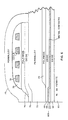
- Figure 6 is a cross-section of the essential elements of a magnetoresistive sensor.
- a layer 62 of oxide preferably aluminium oxide, is deposited upon a soft magnetic substrate 60, preferably NiZn.
- magnetoresistive sensor material 64 is deposited in a magnetic field and patterned. Exchange-bias material may then be deposited and patterned if desired.
- Metal contacts 66 are then deposited on the magnetoresistive sensor material 64.
- a second layer of oxide 68 is then deposited. The two oxide layers 62,68 comprise a read gap.
- a layer of polyimide or photo resist 70 is then deposited and patterned as shown to remove the layer adjacent a gap end of the magnetoresistive head.
- a layer 72 of ferromagnetic material is laid down, preferably of NiFe (Permalloy).
- This layer 72 comprises a trailing pole/shield.
- a write gap oxide layer 75 of, for example, aluminium oxide or silicon dioxide, is deposited followed by a second layer 74 of polyimide or photo resist.
- Metal coils 78 are deposited and patterned.
- Two layers 76 of polyimide or photo resist are deposited and patterned to remove the portion not adjacent the coils 78.
- a final layer 79 of a ferromagnetic material comprises the leading pole/shield and is deposited to encompass the coils and contact the layer 72 to form a continuous flux path.
- the magnetoresistive sensor is formed, it is typically sealed in a suitable non-magnetic material and the gap end processed, e.g. by lapping to expose the end gap or gaps and providing a reliable gap height.
- Figure 7 is an end view of the essential elements of a magnetoresistive sensor. Spacing layers are omitted for clarity. Shown in the Figure are the substrate 60, the magnetoresistive sensor material 64, its lateral metal contact 66 defining a central sense current region 65 of length L, and the ferromagnetic trailing pole/shield 72, and the leading pole/shield 79.
- the length of the leading pole/shield 79 defines the written track width via magnetic mirroring with the trailing pole/shield 72. This length corresponds to the length L (plus a processing guard band wherein the length L is intentionally made smaller than the written track width to avoid possible cross talk) of the central sense current region 65 of the magnetoresistive sensor material 64.
- the magnetoresistive sensor material is longer than a track width to assist in providing a stable single domain in the central sense current region 65. It is essential that the trailing pole/shield 72 is as long as the magnetoresistive sensor material 64 to shield it completely from side fringing fields originating during the writing process. This makes the leading and trailing poles/shields 79,72 of different lengths. However, it has been discovered that this does not affect the written track width, which is defined by the length of the leading pole/shield 79 and the above mentioned mirroring effects.
- linear operation of a magnetoresistive sensor is desirable.
- linearisation either requires the canting of the easy axis magnetisation vector or the canting of the current vector.
- Canting of the magnetisation vector typically increases anisotropy and reduces the range of resistivity change and thus sensitivity of the magnetoresistive sensor.
- Canting the current likewise causes a comparable loss in sensitivity as better illustrated in Figure 8.
- Figure 8 shows a typical canted current biasing technique wherein conductors 80,82, intimately contacting a magnetoresistive strip 92 of length L provide a canted current from a source 88 generally in the direction L eff between the contacts.
- the current direction is generally perpendicular to the surfaces 84,86 of the conductors. These surfaces are generally canted at an angle of ⁇ B of between 40° and 45° for greatest linearity and sensitivity.
- the change in resistivity is sensed by means 90 (which can be a voltage sensor if the source 88 is a constant current source, a transimpedance current sensor if the source 88 is a constant voltage source, or a power sensor if the source 88 is a "soft" source).
- the change in resistivity is generally proportional to the length L eff which is less than the length L between the conductors in the longitudinal direction.
- the length L is approximately the track width of one track and defines the length of the sense current region.
- the sensitivity of the magnetoresistive sensor is reduced by the ratio L eff /L.
- Making L eff comparable to track width is not desirable because the length L would then be long enough to pick up significant cross talk from adjacent tracks.
- Figure 9 shows an improved canted magnetoresistive sensor 94 according to the present invention which relaxes the cant of the surfaces 84,86 of the contacts 80,82 to an angle ⁇ B ⁇ of approximately 50°. This substantially increases L eff and thereby sensitivity while maintaining the approximately 40° to 45° angle with the easy axis.
- the magnetoresistive sensor is patterned such that its easy axis is itself canted by an angle ⁇ EA of approximately 10°.
- the surfaces 84,86 are each canted at an angle ⁇ B ⁇ which is preferably 50°.
- a lower edge 96 of the magnetoresistive sensor is parallel to the magnetic disk surface as in the prior art but an upper edge 98 is patterned at an angle of ⁇ P thereto to give a resultant easy axis magnetisation vector M at an angle ⁇ EA of approximately 10° to the lower edge 96.
- the magnetoresistive sensor 94 is formed from a bulk film deposited on a suitable substrate in an uniform magnetic field directed parallel to the lower edge 96.
- the bulk film is thereafter patterned using conventional lithographic techniques to form the pattern illustrated with the upper edge 98 forming an upwardly extending angle with the lower edge 96.
- This shape inherently cants the easy axis magnetisation vector M upwards, though to a lesser degree than the angle of the upper edge 98.
- the strength of the undeflected easy axis vector with the size, length, thickness, and composition of the magnetoresistive material with the angle of the upper edge to the lower edge will have to be balanced.
- the magnetoresistive sensor 94 is composed of 80:20 NiFe alloy, approximately 500 angstroms thick, with L approximately equal to 9 microns, h (the height of the magnetoresistive sensor at a point 104) approximately equal to 8 microns, and ⁇ P is 10°, ⁇ B ⁇ is 50° and ⁇ EA is 10°.
- Figure 10 shows an example of a canted easy axis psuedo-ellipsoidal magnetoresistive sensor 100 and its relative orientation with surfaces 84,86 (the conductors 80,82 are not shown in Figure 10).
- the magnetisation vector In order to achieve a proper non-linear signal out of the magnetoresistive sensor, the magnetisation vector must be made to rotate to a greater degree than in the biased case (see Figure 11 for an illustration of the principle).
- the upper portion of Figure 11 shows graphically half the normalised magnetoresistive response.
- the lower portion of Figure 11 shows graphically two disk flux input signals 104,106, the signal 104 representing the input signal to a non-linear magnetoresistive sensor, and the signal 106 representing the input to a linear magnetoresistive sensor. While the two signals 104,106 are shown with greatly different magnitudes, they may actually be of the same magnitude if the relative response of the magnetoresistive sensor is proportional to the relative difference shown. Actually, it may be preferable to adjust the relative response of both the disk and the magnetoresistive sensor.
- the signal 106 passes through states 1, 2, 3 and 4 and the magnetoresistive sensor responds by moving through resistivity states 1 ⁇ , 2 ⁇ , 3 ⁇ and 4 ⁇ (for an oppositely polarised pulse, the states would be on the opposite side of the state 1 ⁇ ).
- the inputs and outputs are linear replications.
- the signal 104 passes through states A to F and the sensor responds with states A ⁇ to F ⁇ (an oppositely polarised signal pulse would result in the same output, but from the other half of the resistivity curve).
- the output is non-linear until region D ⁇ to F ⁇ , where it again becomes a linear replication.
- magnetoresistive sensor comprised of permalloy and a magnetic disk material with sufficient flux to yield the magnetisation vector rotation indicated with a magnetoresistive sensor mounted on a conventional head.
- Figure 12 shows a magnetoresistive sensor 10 of psuedo-ellipsoidal shape with contacts 84,86, a constant current source 88 and a voltage sensor 90.
- This magnetoresistive sensor is preferably mounted in the double gap head of Figures 6 and 7. By providing no biasing whatsoever, the sensor operates in a non-linear mode. Its shape and location in the shielded second gap of the double gap head maintains the magnetoresistive sensor in a single domain state. If this implementation is not robust enough for a given application, then stability can be further enhanced by providing exchange material in regions 110,112 as previously described.
- the other illustrated embodiments of the present invention have the easy magnetisation axis canted upwardly from a line parallel to a lower edge of the magnetoresistive sensor.
Landscapes
- Physics & Mathematics (AREA)
- Condensed Matter Physics & Semiconductors (AREA)
- General Physics & Mathematics (AREA)
- Engineering & Computer Science (AREA)
- Manufacturing & Machinery (AREA)
- Measuring Magnetic Variables (AREA)
- Hall/Mr Elements (AREA)
- Magnetic Heads (AREA)
Applications Claiming Priority (2)
| Application Number | Priority Date | Filing Date | Title |
|---|---|---|---|
| US1520387A | 1987-02-17 | 1987-02-17 | |
| US15203 | 1987-02-17 |
Publications (3)
| Publication Number | Publication Date |
|---|---|
| EP0279537A2 true EP0279537A2 (de) | 1988-08-24 |
| EP0279537A3 EP0279537A3 (en) | 1990-01-10 |
| EP0279537B1 EP0279537B1 (de) | 1993-12-29 |
Family
ID=21770085
Family Applications (1)
| Application Number | Title | Priority Date | Filing Date |
|---|---|---|---|
| EP88300685A Expired - Lifetime EP0279537B1 (de) | 1987-02-17 | 1988-01-27 | Magnetoresistiver Sensor und Verfahren zu seiner Herstellung |
Country Status (5)
| Country | Link |
|---|---|
| EP (1) | EP0279537B1 (de) |
| JP (1) | JPH0721848B2 (de) |
| AU (1) | AU1136488A (de) |
| CA (1) | CA1299284C (de) |
| DE (1) | DE3886562T2 (de) |
Cited By (4)
| Publication number | Priority date | Publication date | Assignee | Title |
|---|---|---|---|---|
| WO1990007179A1 (en) * | 1988-12-16 | 1990-06-28 | Eastman Kodak Company | Thin film magnetic element having a rhombic shape |
| EP0598342A1 (de) * | 1992-11-16 | 1994-05-25 | Read-Rite Corporation | Magnetoresistiver Sensorkopf mit zwei Elementen |
| WO1998034231A1 (en) * | 1997-02-05 | 1998-08-06 | Motorola, Inc. | Mram with aligned magnetic vectors |
| EP0759202A4 (de) * | 1995-03-09 | 1999-12-22 | Quantum Corp | Als spin-valve-typ geformter magnetoresistiver übertrager und dessen herstellungsverfahren das eine domänenstabilisierungstechnik enthält |
Families Citing this family (8)
| Publication number | Priority date | Publication date | Assignee | Title |
|---|---|---|---|---|
| JPH07202294A (ja) * | 1993-12-28 | 1995-08-04 | Nec Corp | 磁気抵抗効果素子 |
| JP3180785B2 (ja) | 1998-11-27 | 2001-06-25 | 日本電気株式会社 | ヨーク型磁気抵抗効果ヘッド、ヨーク型磁気抵抗効果複合薄膜ヘッドおよび磁気記憶装置 |
| US6545906B1 (en) | 2001-10-16 | 2003-04-08 | Motorola, Inc. | Method of writing to scalable magnetoresistance random access memory element |
| US7095646B2 (en) | 2002-07-17 | 2006-08-22 | Freescale Semiconductor, Inc. | Multi-state magnetoresistance random access cell with improved memory storage density |
| US6956763B2 (en) | 2003-06-27 | 2005-10-18 | Freescale Semiconductor, Inc. | MRAM element and methods for writing the MRAM element |
| US6967366B2 (en) | 2003-08-25 | 2005-11-22 | Freescale Semiconductor, Inc. | Magnetoresistive random access memory with reduced switching field variation |
| US7129098B2 (en) | 2004-11-24 | 2006-10-31 | Freescale Semiconductor, Inc. | Reduced power magnetoresistive random access memory elements |
| JP6186252B2 (ja) * | 2013-11-13 | 2017-08-23 | アルプス電気株式会社 | 磁気センサ |
Family Cites Families (4)
| Publication number | Priority date | Publication date | Assignee | Title |
|---|---|---|---|---|
| US4103315A (en) * | 1977-06-24 | 1978-07-25 | International Business Machines Corporation | Antiferromagnetic-ferromagnetic exchange bias films |
| JPS56143512A (en) * | 1980-04-05 | 1981-11-09 | Tdk Corp | Magnetic head |
| US4504880A (en) * | 1982-08-09 | 1985-03-12 | International Business Machines Corporation | Integrated magnetic recording head assembly including an inductive write subassembly and a magnetoresistive read subassembly |
| US4639806A (en) * | 1983-09-09 | 1987-01-27 | Sharp Kabushiki Kaisha | Thin film magnetic head having a magnetized ferromagnetic film on the MR element |
-
1987
- 1987-10-15 JP JP62260743A patent/JPH0721848B2/ja not_active Expired - Fee Related
- 1987-10-26 CA CA000550209A patent/CA1299284C/en not_active Expired - Fee Related
-
1988
- 1988-01-27 EP EP88300685A patent/EP0279537B1/de not_active Expired - Lifetime
- 1988-01-27 DE DE88300685T patent/DE3886562T2/de not_active Expired - Fee Related
- 1988-02-05 AU AU11364/88A patent/AU1136488A/en not_active Abandoned
Cited By (4)
| Publication number | Priority date | Publication date | Assignee | Title |
|---|---|---|---|---|
| WO1990007179A1 (en) * | 1988-12-16 | 1990-06-28 | Eastman Kodak Company | Thin film magnetic element having a rhombic shape |
| EP0598342A1 (de) * | 1992-11-16 | 1994-05-25 | Read-Rite Corporation | Magnetoresistiver Sensorkopf mit zwei Elementen |
| EP0759202A4 (de) * | 1995-03-09 | 1999-12-22 | Quantum Corp | Als spin-valve-typ geformter magnetoresistiver übertrager und dessen herstellungsverfahren das eine domänenstabilisierungstechnik enthält |
| WO1998034231A1 (en) * | 1997-02-05 | 1998-08-06 | Motorola, Inc. | Mram with aligned magnetic vectors |
Also Published As
| Publication number | Publication date |
|---|---|
| DE3886562T2 (de) | 1994-04-21 |
| EP0279537A3 (en) | 1990-01-10 |
| AU1136488A (en) | 1988-08-18 |
| EP0279537B1 (de) | 1993-12-29 |
| JPS63205584A (ja) | 1988-08-25 |
| DE3886562D1 (de) | 1994-02-10 |
| JPH0721848B2 (ja) | 1995-03-08 |
| CA1299284C (en) | 1992-04-21 |
Similar Documents
| Publication | Publication Date | Title |
|---|---|---|
| EP0279536B1 (de) | Magnetoresistiver Kopf und Verfahren zu seiner Herstellung | |
| EP0279535B1 (de) | Kopf mit einem magnetoresistiven Aufnehmer | |
| US4967298A (en) | Magnetic head with magnetoresistive sensor, inductive write head, and shield | |
| US4891725A (en) | Magnetoresistive sensor having antiferromagnetic exchange-biased ends | |
| US4052748A (en) | Magnetoresistive magnetic head | |
| US6801411B1 (en) | Dual stripe spin valve sensor without antiferromagnetic pinning layer | |
| US5084794A (en) | Shorted dual element magnetoresistive reproduce head exhibiting high density signal amplification | |
| GB2146482A (en) | Thin film magnetic head | |
| US5880912A (en) | Magnetic head with biased GMR element and sense current compensation | |
| EP0279537B1 (de) | Magnetoresistiver Sensor und Verfahren zu seiner Herstellung | |
| US5475550A (en) | Enhanced cross-talk suppression in magnetoresistive sensors | |
| JPH0773416A (ja) | Mr形読出しトランスジューサおよびその読出し方法 | |
| US5491606A (en) | Planar magnetoresistive head with an improved gap structure | |
| US6597545B2 (en) | Shield design for magnetoresistive sensor | |
| US5959809A (en) | Magnetoresistive head and method of manufacturing the same and magnetic recording apparatus | |
| JPS6227449B2 (de) | ||
| US6028749A (en) | Magnetic head having a multilayer structure and method of manufacturing the magnetic head | |
| JPH0473210B2 (de) | ||
| JPH0719343B2 (ja) | 磁気抵抗型磁気ヘツドの製造方法 | |
| JPH08203032A (ja) | 磁気抵抗効果再生ヘッド | |
| JPH0441415B2 (de) | ||
| JPS63205585A (ja) | 磁気低抗センサ細片 | |
| JPS61196418A (ja) | 薄膜磁気ヘツド | |
| JPS6134577Y2 (de) | ||
| JP2583851B2 (ja) | 磁気抵抗型磁気ヘツド |
Legal Events
| Date | Code | Title | Description |
|---|---|---|---|
| PUAI | Public reference made under article 153(3) epc to a published international application that has entered the european phase |
Free format text: ORIGINAL CODE: 0009012 |
|
| AK | Designated contracting states |
Kind code of ref document: A2 Designated state(s): DE FR GB |
|
| PUAL | Search report despatched |
Free format text: ORIGINAL CODE: 0009013 |
|
| AK | Designated contracting states |
Kind code of ref document: A3 Designated state(s): DE FR GB |
|
| 17P | Request for examination filed |
Effective date: 19900615 |
|
| RAP1 | Party data changed (applicant data changed or rights of an application transferred) |
Owner name: SEAGATE TECHNOLOGY INTERNATIONAL |
|
| 17Q | First examination report despatched |
Effective date: 19920114 |
|
| GRAA | (expected) grant |
Free format text: ORIGINAL CODE: 0009210 |
|
| AK | Designated contracting states |
Kind code of ref document: B1 Designated state(s): DE FR GB |
|
| REF | Corresponds to: |
Ref document number: 3886562 Country of ref document: DE Date of ref document: 19940210 |
|
| ET | Fr: translation filed | ||
| PLBE | No opposition filed within time limit |
Free format text: ORIGINAL CODE: 0009261 |
|
| STAA | Information on the status of an ep patent application or granted ep patent |
Free format text: STATUS: NO OPPOSITION FILED WITHIN TIME LIMIT |
|
| 26N | No opposition filed | ||
| PGFP | Annual fee paid to national office [announced via postgrant information from national office to epo] |
Ref country code: FR Payment date: 19951222 Year of fee payment: 9 |
|
| PG25 | Lapsed in a contracting state [announced via postgrant information from national office to epo] |
Ref country code: FR Effective date: 19970930 |
|
| REG | Reference to a national code |
Ref country code: FR Ref legal event code: ST |
|
| REG | Reference to a national code |
Ref country code: GB Ref legal event code: 732E |
|
| REG | Reference to a national code |
Ref country code: GB Ref legal event code: IF02 |
|
| PGFP | Annual fee paid to national office [announced via postgrant information from national office to epo] |
Ref country code: GB Payment date: 20040106 Year of fee payment: 17 |
|
| PGFP | Annual fee paid to national office [announced via postgrant information from national office to epo] |
Ref country code: DE Payment date: 20040129 Year of fee payment: 17 |
|
| PG25 | Lapsed in a contracting state [announced via postgrant information from national office to epo] |
Ref country code: GB Free format text: LAPSE BECAUSE OF NON-PAYMENT OF DUE FEES Effective date: 20050127 |
|
| PG25 | Lapsed in a contracting state [announced via postgrant information from national office to epo] |
Ref country code: DE Free format text: LAPSE BECAUSE OF NON-PAYMENT OF DUE FEES Effective date: 20050802 |
|
| GBPC | Gb: european patent ceased through non-payment of renewal fee |
Effective date: 20050127 |