EP0280044A2 - Appareil à plasma - Google Patents
Appareil à plasma Download PDFInfo
- Publication number
- EP0280044A2 EP0280044A2 EP88101007A EP88101007A EP0280044A2 EP 0280044 A2 EP0280044 A2 EP 0280044A2 EP 88101007 A EP88101007 A EP 88101007A EP 88101007 A EP88101007 A EP 88101007A EP 0280044 A2 EP0280044 A2 EP 0280044A2
- Authority
- EP
- European Patent Office
- Prior art keywords
- microwave
- plasma
- set forth
- plasma apparatus
- laser
- Prior art date
- Legal status (The legal status is an assumption and is not a legal conclusion. Google has not performed a legal analysis and makes no representation as to the accuracy of the status listed.)
- Granted
Links
Images


Classifications
-
- H—ELECTRICITY
- H01—ELECTRIC ELEMENTS
- H01S—DEVICES USING THE PROCESS OF LIGHT AMPLIFICATION BY STIMULATED EMISSION OF RADIATION [LASER] TO AMPLIFY OR GENERATE LIGHT; DEVICES USING STIMULATED EMISSION OF ELECTROMAGNETIC RADIATION IN WAVE RANGES OTHER THAN OPTICAL
- H01S3/00—Lasers, i.e. devices using stimulated emission of electromagnetic radiation in the infrared, visible or ultraviolet wave range
- H01S3/10—Controlling the intensity, frequency, phase, polarisation or direction of the emitted radiation, e.g. switching, gating, modulating or demodulating
- H01S3/102—Controlling the intensity, frequency, phase, polarisation or direction of the emitted radiation, e.g. switching, gating, modulating or demodulating by controlling the active medium, e.g. by controlling the processes or apparatus for excitation
- H01S3/104—Controlling the intensity, frequency, phase, polarisation or direction of the emitted radiation, e.g. switching, gating, modulating or demodulating by controlling the active medium, e.g. by controlling the processes or apparatus for excitation in gas lasers
-
- H—ELECTRICITY
- H01—ELECTRIC ELEMENTS
- H01J—ELECTRIC DISCHARGE TUBES OR DISCHARGE LAMPS
- H01J37/00—Discharge tubes with provision for introducing objects or material to be exposed to the discharge, e.g. for the purpose of examination or processing thereof
- H01J37/32—Gas-filled discharge tubes
- H01J37/32009—Arrangements for generation of plasma specially adapted for examination or treatment of objects, e.g. plasma sources
- H01J37/32192—Microwave generated discharge
-
- H—ELECTRICITY
- H01—ELECTRIC ELEMENTS
- H01J—ELECTRIC DISCHARGE TUBES OR DISCHARGE LAMPS
- H01J37/00—Discharge tubes with provision for introducing objects or material to be exposed to the discharge, e.g. for the purpose of examination or processing thereof
- H01J37/32—Gas-filled discharge tubes
- H01J37/32009—Arrangements for generation of plasma specially adapted for examination or treatment of objects, e.g. plasma sources
- H01J37/32321—Discharge generated by other radiation
- H01J37/32339—Discharge generated by other radiation using electromagnetic radiation
-
- H—ELECTRICITY
- H01—ELECTRIC ELEMENTS
- H01S—DEVICES USING THE PROCESS OF LIGHT AMPLIFICATION BY STIMULATED EMISSION OF RADIATION [LASER] TO AMPLIFY OR GENERATE LIGHT; DEVICES USING STIMULATED EMISSION OF ELECTROMAGNETIC RADIATION IN WAVE RANGES OTHER THAN OPTICAL
- H01S3/00—Lasers, i.e. devices using stimulated emission of electromagnetic radiation in the infrared, visible or ultraviolet wave range
- H01S3/02—Constructional details
- H01S3/03—Constructional details of gas laser discharge tubes
- H01S3/0315—Waveguide lasers
-
- H—ELECTRICITY
- H01—ELECTRIC ELEMENTS
- H01S—DEVICES USING THE PROCESS OF LIGHT AMPLIFICATION BY STIMULATED EMISSION OF RADIATION [LASER] TO AMPLIFY OR GENERATE LIGHT; DEVICES USING STIMULATED EMISSION OF ELECTROMAGNETIC RADIATION IN WAVE RANGES OTHER THAN OPTICAL
- H01S3/00—Lasers, i.e. devices using stimulated emission of electromagnetic radiation in the infrared, visible or ultraviolet wave range
- H01S3/09—Processes or apparatus for excitation, e.g. pumping
- H01S3/097—Processes or apparatus for excitation, e.g. pumping by gas discharge of a gas laser
- H01S3/0975—Processes or apparatus for excitation, e.g. pumping by gas discharge of a gas laser using inductive or capacitive excitation
-
- H—ELECTRICITY
- H05—ELECTRIC TECHNIQUES NOT OTHERWISE PROVIDED FOR
- H05H—PLASMA TECHNIQUE; PRODUCTION OF ACCELERATED ELECTRICALLY-CHARGED PARTICLES OR OF NEUTRONS; PRODUCTION OR ACCELERATION OF NEUTRAL MOLECULAR OR ATOMIC BEAMS
- H05H1/00—Generating plasma; Handling plasma
- H05H1/24—Generating plasma
- H05H1/46—Generating plasma using applied electromagnetic fields, e.g. high frequency or microwave energy
Definitions
- the present invention relates to a plasma apparatus which generates plasma utilizing microwave discharge and performs laser excitation and can be utilized in plasma processing.
- FIG. 1 is a sectional view of a gas laser apparatus in the prior art disclosed, for example, in Journal of Applied Physics, vol. 49, No. 7, July 1978, p. 3753, and FIG. 2 is a sectional view taken in line A-A in FIG. 1.
- numeral 300 designates a waveguide for transmitting microwave
- numeral 301 designates a waveguide taper provided on a portion of the waveguide 300
- numeral 302 designates a laser discharge tube of Pyrex glass installed in a space of the waveguide taper
- numeral 303 designates a laser gas inlet port provided on an end of the laser discharge tube 302
- numeral 304 designates a laser gas outlet port provided also on an end of the laser discharge tube 302
- numeral 305 designates a cooling gas feed tube installed to surround the laser discharge tube 30
- numeral 306 designates a cooling gas inlet port provided on an end of the cooling gas feed tube 305
- numeral 307 designates a cooling gas outlet port provided also on an end of the cooling gas feed tube 305
- numeral 308 designates Brewster windows installed on both ends of the laser discharge tube 302
- numeral 309 designates a cathode for DC discharge
- numeral 310 designates an anode also for DC discharge.
- a laser gas such as CO2 laser gas is introduced from the laser gas inlet port 303 into the laser discharge tube 302, and on the other hand microwave of TE10 mode is excited in the waveguide 300. Since the waveguide 300 has the waveguide taper 301 on inside and the inner diameter of the waveguide 300 becomes minimum at the installation position of the laser discharge tube 302, the electric field intensity of the microwave becomes maximum in this position.
- the strong microwave field causes discharge breakdown of the laser gas within the laser discharge tube 302 and generates plasma and excites the laser medium.
- N2 gas of low temperature flows in the cooling gas feed tube 305 at high speed and the laser discharge tube 302 is cooled from outside and the discharge condition such as pressure of the laser gas is suitably selected thereby the laser oscillation condition is obtained, and further mirrors for laser oscillation (not shown) are installed on outside of the Brewster windows 308 thereby the laser oscillation is performed.
- the closed laser discharge tube 302 since the closed laser discharge tube 302 is used, if plasma with conductive property is generated, microwave mode of coaxial mode using plasma in the laser discharge tube 302 as the inner conductor becomes predominant and the microwave field in the plasma becomes electric field which component parallel to the tube wall of the discharge tube 302 is main component, thereby microwave entering the plasma substantially becomes mode being incident perpendicularly to the tube wall of the laser discharge tube 302, i.e., the plasma boundary.
- the microwave field is decreased from the discharge tube wall towards inside, but since the discharge plasma has constant-voltage characteristics, the current density varies significantly depending on slight variation of the electric field.
- FIG. 311 designates electric line of force of the microwave electric field
- numeral 312 designates plasma.
- uneven plasma as shown in FIG. 3 is generated, it is difficult that discharge as a whole is made suitable for the laser excitation.
- the laser resonator mode and the plasma are not overlapped with each other thereby the laser output or efficiency becomes low.
- optical waveguide type gas laser apparatus where laser gas is filled in a space acting as an optical waveguide to guide generated laser rays, and plasma is generated in the laser gas by discharge so as to perform laser excitation.
- FIG. 4 is a sectional view of an optical waveguide type gas laser apparatus in the prior art disclosed, for example, in Japanese patent application laid-open No. 54-103692
- FIG. 5 is a sectional view taken along line B-B in FIG. 4.
- numerals 321, 322 designate a pair of long dielectrics opposite to each other
- numerals 323, 324 designate a pair of long electrodes opposite to each other between these dielectrics 321, 322 with a prescribed spacing
- numeral 325 designates a discharge space where all sides are defined by these dielectrics 321, 322 and electrodes 323, 324 and laser gas is filled therein so as to perform laser excitation by discharge
- numeral 326 designates a block of material with high thermal conductivity, on which these dielectrics 321, 322 and electrodes 323, 324 are installed
- numeral 327 designates a total reflection mirror arranged on one end of the discharge space 325
- numeral 328 designates a partial transmission mirror arranged on other end of the discharge space 3
- Laser gas is introduced into the discharge space 325, and high-frequency voltage is supplied between the electrodes 323 and 324 from the high-frequency voltage source 329.
- the strong high-frequency electric field is applied to the laser gas in the discharge space 325, and the discharge breakdown of the laser gas is produced by the high-frequency electric field and plasma is generated and the laser excitation is performed.
- the generated laser rays pass through the discharge space 325 as optical waveguide and are reflected between the total reflection mirror 327 and the partial transmission mirror 328 arranged on both ends of the discharge space 325, and a part of the laser rays is taken to outside by the partial transmission mirror 328.
- the optical waveguide type gas laser apparatus in the prior art is constituted as above described, it is difficult that frequency of the high-frequency voltage applied between the electrodes 323 and 324 is made higher than certain extent. Moreover, as the frequency of the high-frequency voltage is increased, the discharge in the discharge space 325 is concentrated to surface portion of the dielectrics 321, 322 arranged on both sides of the discharge space 325, thereby uniform plasma cannot be obtained and it is difficult that the discharge space 325 as a whole is made suitable for the laser excitation.
- a first object of the present invention is to provide a plasma apparatus wherein plasma being uniform in space and stable is generated, and laser operation of high efficiency and large output is possible, and further filling of the plasma generating medium is simple.
- a second object of the present invention is to provide a plasma apparatus of high efficiency and long life, wherein a wall surface of a discharge space is protected, and deterioration of a plasma generating medium is prevented.
- a third object of the present invention is to provide a plasma apparatus of large diameter, wherein uniform discharge is obtained even at a discharge space of large area.
- a fourth object of the present invention is to provide a plasma apparatus wherein microwave discharge plasma becomes uniform in space even in an optical waveguide type gas laser apparatus.
- a fifth object of the present invention is to provide a plasma apparatus wherein generated microwave discharge plasma is made uniform in space, and cooling efficiency of a discharge tube is improved, and further laser operation of high efficiency and large output is possible.
- a sixth object of the present invention is to provide a plasma apparatus wherein a plasma generating medium filled in a discharge space can be prevented from leakage.
- a seventh object of the present invention is to provide a power source apparatus of small size, which can be used as a power source of a plasma apparatus and does not require a high-voltage power source for pulse control.
- a plasma generating medium to generate plasma by microwave discharge is filled in a space formed between a conductor wall to constitute a part of a microwave circuit such as a waveguide and dielectrics installed opposite to the conductor wall, and the microwave circuit forms microwave mode having vertical electric field component at the boundary between the dielectrics and the plasma.
- the conductor wall having higher conductivity than that of the plasma exists in opposition to dielectrics as a microwave incident window, the end current of the incident microwave flows through the conductor wall, thereby current penetrating between the dielectrics and the conductor wall flows in the plasma so as to generate the plasma being uniform in space.
- a plasma apparatus also generates plasma by microwave discharge in pulse microwave. Thereby the plasma becomes further uniform in space.
- microwave excited in a microwave circuit is made pulse microwave where quiescent time is shorter than thermal time constant of a plasma generating medium, for example, CO2 laser gas. Consequently, in the plasma apparatus of this invention, the plasma can be made uniform also in time.
- a plasma generating medium for example, CO2 laser gas
- a conductor wall surface to constitute the space is coated with a ceramic layer so as to protect the wall surface, thereby deterioration of a plasma generating medium is prevented and plasma discharge at high efficiency and long life becomes possible.
- a reservoir tank communicating with the space is installed to store a plasma generating medium, thereby a compact plasma apparatus with high efficiency, large output and long life can be obtained.
- first and second dielectrics are arranged to a bottom surface and a side surface of the space constituted by the conductor wall, thereby plasma with high uniformity can be generated even in the discharge space of large area.
- a space as an optical waveguide is formed by a conductor wall to constitute a part of a microwave circuit and dielectrics installed opposite to the conductor wall, and a laser gas as a plasma generating medium is filled in the space, and further microwave is incident thereto using the dielectrics as a microwave incident wall, thereby microwave mode having vertical electric field component is formed at the boundary between the dielectrics and the plasma generated in the laser gas.
- a portion other than the dielectrics of the space is partially formed by a gas permeable member, and circulation means for circulating the plasma generating medium within the space is installed through the gas permeable member.
- circulation means for circulating the plasma generating medium within the space is installed through the gas permeable member.
- the dielectrics and a part of a microwave formed the conductor wall are bonded and sealed by an epoxy adhesive agent or metal seal such as brazing. Consequently, the plasma generating medium filled in the discharge space is prevented from leakage, and stable laser oscillation becomes possible.
- a metallized layer is provided on a surface of the dielectrics opposite to the discharge space, and other surface of the metallized layer faces directly to a cooling water path. Consequently, cooling water in the cooling water path installed in a ridge is contacted directly with the metallized layer provided on the dielectrics, thereby heat generated in a laser gas such as CO2 gas is removed efficiently and the temperature rise of the laser gas such as CO2 gas is prevented.
- an opening frame of a groove to constitute a discharge space is formed not in an edge-shaped surface but in an arc-shaped surface, thereby concentration of the electric field to the opening frame can be prevented hence generation of uneven plasma in the discharge space can be prevented further effectively.
- a metallized layer is provided on the dielectrics near position corresponding to the opening edge portion of the groove to constitute the discharge space, and the metallized layer shields the electric field of microwave and prevents concentration of the electric field in the opening edge portion so that plasma being uniform in space can be generated stably.
- the microwave transmission path and the microwave circuit are arranged in parallel along the laser optical axis, thereby discharge length which is sufficient to increase laser output and uniform can be secured, and the apparatus as a whole is made compact, and further space factor and control property can be significantly improved in comparison to the prior art.
- FIG. 6 is an appearance view of a gas laser apparatus as an example of plasma apparatuses in a first embodiment of the present invention.
- reference numeral 1 designates a magnetron being a microwave oscillator
- numeral 2 designates a waveguide
- numeral 3 designates a horn waveguide to enlarge width of the waveguide 2
- numeral 4 designates a microwave coupling window
- numeral 5 designates a mirror for laser oscillation
- numeral 6 designates a laser head section.
- FIG. 7 is a sectional view taken in line C-C of FIG. 6 illustrating details of the gas laser apparatus.
- the laser head section 6 has structure of a microwave cavity of ridge waveguide type being a sort of a microwave circuit.
- FIG. 1 designates a magnetron being a microwave oscillator
- numeral 3 designates a waveguide to enlarge width of the waveguide 2
- numeral 4 designates a microwave coupling window
- numeral 5 designates a mirror for laser oscillation
- numeral 7 designates a cavity wall following the microwave coupling window 4
- numerals 8 and 9 designate ridges formed on center portion of section of the cavity wall 7
- numeral 10 designates a groove formed on one ridge 8
- numeral 11 designates a conductor wall to constitute a part of the microwave circuit and the wall surface of the groove 10 is used therefor in this embodiment.
- Numeral 12 designates dielectrics such as alumina installed opposite to the conductor wall 11 for acting as an incident window of microwave
- numeral 13 designates a discharge space formed between the conductor wall 11 and the dielectrics 12 when the dielectrics 12 cover the groove 10, and a laser gas such as CO2 laser gas being a plasma generating medium is filled in the discharge space 13.
- Numeral 14 designates a cooling water path formed in the ridges 8 and 9.
- microwave generated by the magnetron 1 passes through the waveguide 2 and is widened by the horn waveguide 3. After taking impedance matching by the microwave coupling window 4 for good efficiency, the microwave is coupled with the laser head section 6. Since the laser head section 6 has cross-section of ridge cavity form as shown in FIG. 7, the microwave is concentrated between the ridges 8 and 9. The strong electromagnetic field of the concentrated microwave causes the discharge breakdown of the laser gas filled in the discharge space 13 and generates plasma and excites the laser medium. Then a cooling water flows in the cooling water path 14 so as to cool the discharge plasma, and discharge conditions such as pressure of the laser gas are suitably selected thereby the laser oscillation conditions can be obtained. Then a laser resonator is formed by the mirror 5 in FIG. 6 and another mirror (not shown) thereby the laser oscillation rays can be obtained.
- microwave discharge is performed in the discharge space 13 formed between the conductor wall 11 to constitute a part of the microwave circuit and the dielectrics 12 as a microwave incident window installed opposite to the conductor wall 11, it follows that the entering of the microwave is performed only from one side of the plasma. Consequently, such phenomenon does not occur that microwave mode of coaxial mode using the plasma as inner conductor becomes predominant, thereby discharge by expected microwave mode can be performed.
- the microwave circuit forms microwave mode having electric field component being perpendicular to the boundary between the dielectrics 12 and the plasma as in the ridge cavity shown in FIG. 7, since the dielectrics 12 and the conductor wall 11 are installed opposite to each other, the microwave mode has the electric field component also perpendicular to the conductor wall 11 thereby the electric field penetrating the plasma is formed.
- the discharge as a whole can be easily made suitable for the laser excitation and also the laser resonator mode and the plasma are overlapped well, thereby the laser oscillation can be obtained at significantly high efficiency and large output in comparison to a gas laser apparatus utilizing microwave discharge in the prior art.
- the dielectrics 12 and the ridge 8 on which the groove 10 is formed are closely contacted with each other in surface and the laser gas is filled therein, when pressure of the laser gas is lower than the atmospheric pressure, for example, in the case of CO2 gas laser apparatus, the external pressure is applied to the dielectrics 12 thereby the laser gas can be easily sealed.
- the closely contacted surface may be bonded by an adhesive agent or separate pressure may be applied from outside, and at any case the laser gas can be sealed quite easily by structure that the groove 10 is covered by the dielectrics 12.
- microwave cavity of ridge waveguide type is used in the microwave circuit in the embodiment as above described, a microwave circuit of other type such as rectangular cavity may be used and similar effect to the above-mentioned effect can be obtained.
- FIG. 9 is a graph illustrating experiment results when the apparatus having the constitution shown in FIG. 6 and FIG. 7 and the discharge length 300 mm is applied to the CO2 laser.
- abscissa indicates microwave input of frequency 2.45 GHz
- ordinate indicates the CO2 laser output and efficiency.
- maximum output 24 W and maximum efficiency 10.5% are obtained, that is, the output becomes larger than the CO2 laser output 15 mW reported in the prior art shown in FIGS. 1 and 2 by three figures or more.
- the CW oscillation can be performed in the apparatus according to the present invention.
- the apparatus since the metal wall to confine the microwave and the discharge plasma are closely contacted with each other, the cooling can be performed from outside of the metal wall freely and effectively. Consequently, the apparatus is favorably applied to a laser where cooling of the laser gas is important, for example, CO2 laser. Moreover, since effect of the magnetic field is not used, the apparatus can be applied also to a high pressure laser such as eximer laser, and a device for generating the magnetic field is not required and therefore the apparatus becomes compact and simple.
- FIG. 10 is sectional views illustrating examples of constitution methods of the discharge space 13 where a microwave cavity or a wave-guide is used as a microwave circuit.
- numeral 11 designates a conductor wall
- numeral 12 designates dielectrics
- numeral 13 designates a discharge space.
- the microwave cavity is partitioned by the dielectrics 12 so as to form the discharge space 13, and the apparatus is advantageous in the easy manufacturing.
- space other than the discharge space 13 is filled with the dielectrics 12, thereby unnecessary discharge in the space other than the discharge space 13 can be prevented.
- FIG. 10 is sectional views illustrating examples of constitution methods of the discharge space 13 where a microwave cavity or a wave-guide is used as a microwave circuit.
- numeral 11 designates a conductor wall
- numeral 12 designates dielectrics
- numeral 13 designates a discharge space.
- the microwave cavity is partitioned by the dielectrics 12 so as to form the discharge space 13 and the apparatus is advantageous in the easy manufacturing.
- the groove formed on the cavity wall is made the discharge space 13, and the apparatus is advantageous in that the discharge space 13 of any size can be formed.
- the ridge 9 is added to the apparatus in FIG. 10(c), and the apparatus in FIG. 10(d) is advantageous in comparison to the apparatus in FIG. 10(c) in that the laser gas of high pressure can be discharged, and the matching becomes easy.
- the dielectrics 12 having a recess are utilized, and the apparatus is advantageous in that the discharge space 13 of any size can be formed using the microwave cavity of standard shape.
- the ridge 9 is added to the apparatus in FIG. 10(e), and the apparatus in FIG. 10(f) is advantageous in comparison to the apparatus in FIG.
- FIGS. 10(e) show utilization in combination of these constitutions.
- the conductor wall 11 to constitute a part of the microwave circuit and the dielectrics 12 installed opposite to the conductor wall 11 are suitably selected, thereby the discharge space 13 can be designed considerably freely, and uniform discharge similar to that shown in FIG. 8 can be obtained.
- FIG. 11 is sectional views illustrating embodiments where a coaxial line or a strip line is used as a microwave circuit.
- FIG. 11(a) shows an embodiment where the outer conductor of the coaxial line is utilized as the conductor wall 11 to constitute a part of the microwave circuit
- FIG. 11(b) shows an embodiment where the inner conductor of the coaxial line is made the conductor wall 11
- FIG. 11(c) shows an embodiment where the strip line is used. Since the coaxial line and the strip line shown in FIG. 11 do not have the cutoff frequency, for example, when the microwave of 245 GHz is used, the apparatus as a whole can take compact apparatus constitution in comparison to the apparatus using the microwave cavity and therefore is advantageous. In each of FIGS. 11(a), (b), (c), of course, various apparatus constitutions corresponding to the constitution methods of the discharge space shown in FIG. 10 can be taken.
- FIG. 12 is sectional views illustrating embodiments where a surface wave line is used as a microwave circuit.
- FIG. 12(a) shows an embodiment where a conductor flat plate is made the conductor wall 11 and a dielectric flat plate is made the dielectrics 12 so that the discharge space 13 is formed and at the same time the surface wave line is constituted
- FIG. 12(b) shows an embodiment where a conductor circular cylinder is made the conductor wall 11 and a dielectric tube surrounding the conductor circular cylinder is made the dielectrics 12 so that the discharge space 13 is formed and at the same time the surface wave line is constituted.
- the microwave circuit and the discharge space can be constituted simultaneously using the minimum components, and the apparatus is simplified and advantageous.
- various apparatus constitutions corresponding to the constitution methods of the discharge space shown in FIG. 10 can be taken.
- FIG. 13 is sectional views illustrating embodiments where a projection 21 is provided on a part of the microwave circuit, and plasma 22 is generated in the strong electromagnetic field formed in a part of the discharge space by the projection 21.
- FIG. 13(a) shows an embodiment where the projection 21 is provided on outside of the discharge space 13
- FIG. 13(b) shows an embodiment where the projection 21 is provided on inside of the discharge space 13.
- the discharge plasma can be concentrated only in a part of the discharge space 13, and a laser apparatus of three-axis orthogonal type can be easily obtained. Also the laser gas of high pressure can be discharged, and the plasma of high discharge power density can be easily generated.
- the laser gas generating plasma by the microwave discharge is filled in a space formed between a conductor wall to constitute a part of a microwave circuit and dielectrics installed opposite to the conductor wall and at the same time the microwave circuit forms microwave mode having the electric field component perpendicular to the boundary between the dielectrics and the plasma, the microwave discharge plasma being uniform in space can be generated and the discharge as a whole can be made suitable for the laser excitation and further the laser resonator mode and the plasma can be overlapped well, thereby the gas laser apparatus of high efficiency and large output can be obtained.
- a groove is formed on the conductor to constitute a part of the microwave circuit and an opening portion of the groove is covered by the dielectrics so as to form a space, and a plasma generating medium is filled in the space, filling of the plasma generating medium into the space can be performed easily.
- plasma being more uniform in space can be generated by microwave discharge of the pulse microwave.
- constitution of the gas laser apparatus in the second embodiment is similar to that of the first embodiment shown in FIGS. 6 and 7. Consequently, the same parts shall be described by designating the same reference numerals.
- a power source to drive a magnetron 1 is constituted as shown in FIG. 14.
- commercial frequency AC power source E is converted into DC by a rectifying and smoothing circuit 25, and the DC is converted into high-frequency AC such as 20 KHz by a DC-AC inverter circuit 26.
- the high-frequency AC is stepped up by a transformer 27, and converted into ripple current of high voltage by a half-wave voltage multiplying rectifier circuit 28 constituted by a capacitor C and diodes D1, D2, and then applied to the magnetron 1.
- Numeral 29 designates a filament power source of the magnetron 1.
- waveform of the microwave generated by the magnetron driven by the power source becomes as shown in FIG. 15. That is, pulse microwave interrupted by high frequency is generated. Pulse duty of the pulse microwave can be made very high value such as 0.1 - 0.4 in comparison to the pulse microwave in the prior art. Consequently, quiescent time of the microwave becomes sufficiently shorter than the thermal time constant of the plasma generating medium, for example, CO2 laser gas. Also the pulse frequency can be made very high such as several tens kHz.
- inverter is used as the power source of the magnetron 1 in the embodiment as above described
- power source of chopper type to be applied to the magnetron 1 from the DC power source of high voltage through switching element may be used so as to generate the pulse microwave.
- the laser apparatus is shown as the plasma apparatus in the embodiment, the invention may be applied to an ion source or a light source plasma processing apparatus, and similar effect can be obtained in that the discharge is made uniform in space and in time.
- the plasma generating medium is filled in a space formed between a conductor wall to constitute a part of the microwave circuit in the plasma apparatus and dielectrics installed opposite to the conductor wall, and the microwave circuit forms microwave mode having component being perpendicular to the boundary with the dielectrics and the pulse microwave is excited in the microwave circuit, thereby the plasma being uniform in space can be obtained.
- the pulse microwave having the quiescent time shorter than the thermal time constant of the plasma generating medium such as CO2 laser gas is excited in the microwave circuit, the plasma being uniform in space and in time can maintained stably for a long time, and the discharge as a whole can be easily made suitable for the laser excitation, and the laser resonator mode and the plasma can be overlapped well, thereby the CO2 gas laser apparatus to enable the laser operation of high efficiency and large output can be obtained.
- FIG. 16 is a circuit diagram of the power source apparatus.
- M designates a magnetron as a non-linear element
- Q1, Q2 designate field effect transistors (hereinafter referred to as "FET") as semiconductor switching element
- PT1, PT2, PT3 designate pulse transformers to apply voltage to gate of the FET Q1, Q2, D1, D2 designate reverse-current blocking diodes
- R3, R4, R5 designate dividing resistors for high voltage
- PG designates a pulse generator.
- Relation between the anode applied voltage and the anode current in the magnetron M becomes as shown in FIG. 17, and the current does not flow at the cutoff voltage V z or less. Consequently, if values of the dividing resistors R3 - R5 are determined so that V oM ⁇ V z , the magnetron M does not act when the FET Q1 - Q2 are turned off.
- the values of the dividing resistors R3 - R5 are determined so that relation of withstand voltage of the FET Q1, Q2 to V DSS (drain-source voltage) becomes V oQ1 , V oQ2 ⁇ V DSS , si voltage over the withstand voltage is not applied to the FET Q1, Q2 when the FET Q1, Q2 are turned off, the FET Q1, Q2 are not broken.
- pulse is applied to the pulse transformer PT3 from the pulse generator PG, the pulse is applied to gate of the FET Q1, Q2 and therefore the FET Q1, Q2 are turned on. Then since the magnetron M is supplied with the power source voltage -E(V) as it is, the magnetron M acts and microwave is generated. Thus every time pulse is applied to the pulse transformer PT3 from the pulse generator PG, the magnetron M acts and the microwave is generated in pulse form. Since the FET Q1, Q2 are connected to the high voltage circuit, they must be insulated to the power source of the pulse generator PG. However, if the insulation withstand voltage of the pulse transformers PT1 - PT3 is made E(V) or more, the pulse generator PG is insulated from the high voltage circuit and therefore can be constituted in ordinary power source potential or the ground potential.
- FIG. 18 is a circuit diagram illustrating another embodiment where one bipolar transistor is used as the semiconductor switching element.
- FIG. 18 the same or similar parts to those of FIG. 16 as hereinbefore described are designated by the same reference numerals.
- Q3 designates one transistor as the switching element
- IP designates an insulation power source.
- the pulse generator PG drives base of the bipolar transistor Q3 thereby the bipolar transistor Q3 is turned on. Also in this case, in similar manner to FIG. 16, values of the dividing resistors R4, R5 may be set so that voltage applied to the magnetron M becomes V z or less at OFF-state of the bipolar transistor Q3, and voltage applied to the bipolar transistor Q3 is its withstand voltage or less. Further, although the pulse generator PG is connected directly to the high voltage circuit, if the power source of the pulse generator PG is made the insulation power source IP where high-voltage insulation is performed by the power source transformer, the high voltage circuit and the primary side of the power source are insulated.
- any power source for the non-linear element or device where current does not flow at voltage less than the prescribed voltage E z , and current flows at the prescribed voltage E z or more can perform similar operation.
- the power source apparatus of the invention in the power source apparatus to drive the nonlinear element or device where current does not flow at voltage less than the prescribed voltage E z and current flows at the prescribed voltage E z or more, since the semiconductor switching element connected in series to the nonlinear element or device controls current flowing from the voltage source to the nonlinear element or device, the power source of high voltage is not required for the control, and the power source apparatus of small size can be obtained, and further the semiconductor switching element with relatively low withstand voltage may be used.
- the wall surface by the conductor of the space in which the laser gas is filled as shown in the first embodiment is coated with a ceramic layer.
- the wall surface of the conductor can be protected, and deterioration of the laser gas can be prevented, and further the laser oscillation at high efficiency and long life becomes possible.
- the ceramic layer 15 is formed by coating. If the ceramic layer 15 is formed in such manner, since the wall surface by the conductor including the conductor wall 11 of the discharge space 13 coated with the ceramic layer 15, the plasma generated by the microwave discharge is not directly contacted with the conductor wall 11 or the like, and the generated plasma is not liable to sputtering and enveloped in the ceramic layer 15 and the dielectrics 12 being inert chemically.
- the plasma apparatus such as the gas laser apparatus of microwave excitation system can be realized at high efficiency and long life.
- thickness of the ceramic layer 15 is sufficiently less than that of the dielectrics 12.
- thickness of the ceramic layer 15 is made 1/10 of that of the dielectrics 12 or less, it has been confirmed that most of the microwave energy is injected from side of the dielectrics 12 of the plasma.
- impedance of the end of the incident microwave is less than impedance of the plasma.
- the laser apparatus using the laser gas including halogen gas having high chemical activation such as an eximer laser apparatus, of course, material which does not react with halogen group should be used as the ceramic layer 15.
- a reservoir tank communicating with the space formed by the conductor wall and the dielectrics is installed, and the plasma generating medium is stored in the reservoir tank, thereby deterioration of the plasma generating medium such as the laser gas is prevented, and the plasma apparatus to enable the plasma operation at high efficiency and large output can be obtained.
- FIG. 19 shows constitution of the apparatus.
- numeral 31 designates a reservoir tank which is formed in the conductor behind the conductor wall 11 of the ridge 8 for storing the laser gas to replace the laser gas within the discharge space 13
- numeral 32 designates one or plural connection penetrating holes to perform communication between the reservoir tank 31 and the discharge space 13
- numeral 33 designates a gas permeable member, for example, by a metal mesh or the like, which is arranged at an opening portion in the discharge space 13 of the connection penetrating hole 32 and makes the laser gas pass and reflects the microwave.
- the laser gas in the discharge space 13 suitably replaces the laser gas in the reservoir tank 31 through the connection penetrating hole 32 and the gas permeable member 33, thereby even if the laser oscillation is performed for a long time, deterioration of the laser gas can be suppressed to minimum and the laser gas is made long life.
- the gas permeable member 33 by the metal mesh or the like is arranged at the opening portion in the discharge space 13 of the connection penetrating hole 32, the microwave mode in the discharge space 13 is not disturbed.
- the gas permeable member to reflect the microwave and to make the laser gas pass is arranged on end portion at side of the discharge space of the connection penetrating hole, if the connection penetrating hole is of cutoff size or less not to transmit the microwave, the gas permeable member may be omitted and similar effects to that of the above embodiment are obtained.
- the plasma generating medium such as laser gas to generate the plasma by the microwave discharge is filled in the space formed between the conductor wall formed on a part of the microwave circuit and the dielectrics installed opposite to the conductor wall, and the plasma generating medium suitably replaces the medium stored in the reservoir tank, and further the microwave circuit forms the microwave mode having the electric field distribution orthogonal to the boundary between the dielectrics and the plasma, the plasma being uniform in space can be stably maintained for a long time and the discharge as a whole can be made suitable for the laser excitation. Further, since deterioration of the plasma producing medium can be prevented without adding a large-scale apparatus at outside for changing the plasma generating medium, the compact plasma apparatus can be obtained at high efficiency, large output and long life.
- FIG. 20 shows the gas laser apparatus according to the fifth embodiment.
- FIG. 20 common parts to those in FIG. 7 of the first embodiment are designated by the same reference numerals.
- numeral 41 designates a recess formed on one ridge 8
- numeral 42 designates a conductor wall which constitutes a part of the microwave circuit and forms a bottom surface of the recess 41
- numeral 43 designates a second conductor wall which forms side surface of the recess 41.
- Numeral 44 designates first dielectrics, for example, by alumina, which covers an opening portion of the recess 41 and is opposite to the first conductor wall 42 and acts as an incident window of microwave.
- Numeral 45 designates second dielectrics, for example, by alumina, which is arranged on the wall surface of the second conductor wall 43.
- Numeral 46 designates a discharge space which is formed between the first dielectrics 44 and the second dielectrics 45 when the first conductor wall 42 covers the opening portion of the recess, and in which the plasma generating medium such as CO2 laser gas is filled, and numeral 14 designates a cooling water path formed on the ridge 8 and the ridge 9.
- Main part of the laser excitation operation of the fifth embodiment is similar to the case of the first embodiment described in FIG. 7.
- microwave discharge is performed in the discharge space 46 having the first conductor wall 42 to constitute a part of the microwave circuit, and the first dielectrics 44 being an incident window of microwave, which is installed opposite to the first conductor wall 42. Since the microwave is incident to the plasma only from one surface thereof, it does not occur that the microwave mode of the coaxial mode using the plasma as inner conductor becomes predominant, and discharge by expected microwave mode can be performed.
- the microwave circuit forms the microwave mode having the electric field component orthogonal to the boundary between the first dielectrics 44 and the plasma as in the ridge cavity of the laser head section 6 shown in the figure, since the first dielectrics 44 and the first conductor wall 42 are opposite to each other, the electric field component is orthogonal also to the first conductor wall 42 thereby the electric field penetrating the plasma is produced.
- the end current of the incident microwave flows through the first conductor wall 42 and the electric field near the first conductor wall 42 is made forcedly orthogonal to the surface of the first conductor wall 42 thereby the electric field penetrating the generated plasma is maintained. Consequently, the microwave enters into the plasma and the current penetrating the plasma flows and the discharge plasma being uniform in space is generated because of continuity of current.
- the second dielectrics 45 are arranged between the second conductor wall 43 and the plasma within the discharge space 46, and as shown in FIG. 21(c), the second dielectrics 45 weakens the electric line of force 47 directed to the second conductor wall 43 and strengthens the electric line of force 47 directed to the first conductor wall 42 so that the electric field component orthogonal to the first conductor wall 42 becomes predominant. Thereby the uniform discharge in space is obtained and the discharge as a whole can be easily made suitable for the laser excitation.
- the invention may be applied to a plasma processing apparatus, an ion source, a light source or the like, and similar effects to the embodiment can be obtained.
- the first conductor wall with the bottom surface constituting a part of the microwave circuit, and the second conductor wall as the side surface constitute the recess, and an opening portion of the recess is covered with the first dielectrics, and further the plasma generating medium is filled in the space formed by the second dielectrics arranged on the second conductor wall, and the microwave circuit forms the microwave mode having the electric field component orthogonal to the boundary between the plasma and the first dielectrics, thereby the microwave being uniform in space is stably maintained for a long time even at the discharge space of large area, and the plasma apparatus of large diameter to generate plasma having high uniformity in space can be obtained.
- FIG. 22 is a sectional view taken along line X-X in FIG. 7.
- FIG. 22 is a sectional view taken along line X-X in FIG. 7.
- numeral 6 designates a laser head section
- numerals 51 and 52 designate ridges installed on a cavity wall 7 following a microwave coupling window 4
- numeral 53 designates a conductor wall
- numeral 54 designates dielectrics as an incident window of microwave opposite to the conductor wall 53
- numeral 55 designates a discharge space which is formed between the conductor wall 53 and the dielectrics 54 when the dielectrics 54 cover the groove formed on the ridge 51 and in which the laser gas such as CO2 laser gas is filled
- numeral 56 designates a cooling water path formed on the ridge 51 having the conductor wall 53 constituting a part of the microwave circuit and on the ridge 52 opposite to the ridge 51.
- numerals 57, 58 designate a total reflection mirror and a partial transmission mirror respectively arranged opposite to each other on both ends of the discharge space 55, and the discharge space 55 acts also as an optical waveguide having dimension suitable to guide the generated laser rays.
- a cooling water flows in the cooling water path 56 provided on the ridge 51 having the conductor wall 53 constituting a part of the microwave circuit and on the ridge 52 opposite to the ridge 51, and the conductor wall 53 and the dielectrics 54 contacted directly with the laser gas within the discharge space 55 are cooled, thereby the laser gas is cooled efficiently, and saturation of the laser output due to temperature rise of the laser gas is prevented although this becomes a problem particularly in the case of using the CO2 laser gas, and further the optical waveguide type gas laser apparatus can be obtained at high efficiency and large output.
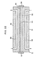
- FIG. 23 is a partial sectional view illustrating the embodiment in such state.
- numerals 51, 52 designate ridges
- numeral 53 designates a conductor wall by the upper surface of the ridge 51
- numeral 54 designates dielectrics provided with a groove at lower surface and held on the ridge 51
- numeral 55 designates a discharge space formed by the groove of the dielectrics 54 and the conductor wall 53 on the upper surface of the ridge 51
- the discharge space 55 also acts as an optical waveguide having dimension suitable to guide the generated laser rays.
- the space being an optical waveguide is formed by the conductor wall constituting a part of the microwave circuit and the dielectrics opposite to the conductor wall, and laser gas is filled in the space and the microwave is entered using the dielectrics as a microwave incident window, thereby the laser excitation by the microwave becomes possible. Furthermore, since the conductor wall having conductivity higher than that of the plasma exists opposite to the dielectrics into which the microwave is entered, the end current of the incident microwave flows through the conductor wall and current penetrating between the dielectrics and the conductor wall flows in the plasma, thereby the uniform plasma in space can be stably maintained in the laser gas.
- FIGS. 24 through 26 show a seventh embodiment where heat of a laser discharge tube is prevented by circulation means.
- FIG. 24 is a sectional front view of the gas laser apparatus. An appearance view of the seventh embodiment is the same as that of the first embodiment shown in FIG. 6, and in FIG. 24, common parts to those in the first embodiment are designated by the same reference numerals and the description shall be omitted.
- numeral 6 designates a laser head section having structure of a microwave cavity of ridge waveguide type
- numeral 1 designates a magnetron
- numeral 2 designates a waveguide
- numeral 3 designates a horn waveguide
- numeral 4 designates a microwave coupling window.
- Numeral 7 designates a cavity wall following the microwave coupling window 4 in the laser head section 6
- numeral 61 designates a ridge installed on center portion of the cavity wall 7
- numeral 62 designates a conductor wall constituting a part of the microwave circuit, and in this embodiment, a flat H-surface opposite to the cavity 7 of the microwave circuit of the microwave cavity structure of ridge waveguide type is used as the conductor wall 62.
- Numeral 63 designates dielectrics, for example, by alumina, which is installed opposite to the conductor wall 62 and acts as a microwave incident window
- numeral 64 designates a discharge space which is formed between the conductor wall 62 and the dielectrics 63 and in which the laser gas such as CO2 laser gas is filled
- numeral 65 designates a gas feed tube communicating with the discharge space 64
- numeral 66 designates a blower as circulation means installed at midway of the gas feed tube 65
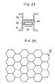
- numeral 67 designates a gas permeable member installed at an opening portion of the gas feed tube 65 to the discharge space 64 for reflecting the microwave, and for example, a honeycomb structure of metal as shown in FIG. 25 is used as the gas permeable member 67.
- the blower 66 is operated and the laser gas within the discharge space 64 is circulated and the discharge plasma is cooled, and at the same time the discharge conditions such as pressure of the laser gas are suitably selected thereby the laser oscillation conditions are obtained. Since the gas permeable member 67 by the metal honeycomb structure shown in FIG. 25 is used in the opening portion of the gas feed tube 65 provided on the conductor wall 62, the laser gas passes through it but the microwave is reflected, thereby the microwave mode within the discharge space 64 is not influenced and the forced circulation of the laser gas by the blower 66 becomes possible. As a result, the discharge plasma being uniform in space is generated.
- the microwave propagating freely in the dielectrics 63 enters into the plasma uniformly from the boundary between the dielectrics 63 and the plasma, and the microwave discharge is not apt to become the arc discharge essentially even at the electrodeless discharge, and further the dielectrics 63 act as the capacitive distribution balast, the discharge plasma being uniform in space can be obtained also in the transverse direction of the plasma. As a result, the discharge being significantly uniform in space can be realized. Since the uniform discharge in space is obtained in such manner, the discharge as a whole can be easily made suitable for the laser excitation.
- the gas laser apparatus can be obtained at high efficiency and large output.
- the gas permeable member 67 is arranged on the conductor wall 62 to form the bottom surface of the discharge space 64, it may be arranged at side wall portion of the discharge space 64.
- FIG. 26 is a partial sectional view illustrating the embodiment in such state.
- a part of the cavity portion of the microwave circuit acts as the gas feed tube, and at the side wall portion of the discharge space 64 between the conductor wall 62 and the dielectrics 63, the gas permeable member 67 formed by the metal honeycomb structure is arranged where the laser gas can pass but the microwave is reflected.
- the blower 66 as circulation means is provided with a heat exchanger 68, thereby heat of the circulated laser gas is forcedly radiated to outside and the plasma is cooled more effectively.
- the honeycomb structure of metal is used as the gas permeable member to reflect the microwave
- the gas permeable member may be a conductor with a number of small holes bored thereon, or a metal mesh may be used, and in any case, similar effects to that of the embodiment can be obtained.
- the laser gas is forcedly circulated and cooled by the circulation means, the plasma being uniform in space can be stably maintained for a long time and saturation of the laser output due to temperature rise of the laser gas also can be prevented, thereby the gas laser apparatus to enable laser operation at high efficiency and large output can be obtained.
- FIGS. 27 through 32 show an eighth embodiment where leakage of the plasma generating medium in the discharge space is prevented by epoxy adhesive agent.
- FIG. 27 shows the same apparatus as the gas laser apparatus of the first embodiment shown in FIG. 7.
- numeral 70 designates epoxy adhesive agent which is applied to whole surface of a portion where the dielectrics 12 and the ridge 8 with the conductor wall 11 are contacted with each other and which bonds and seals both members together so that the air tightness of the discharge space 13 is improved. Thereby leakage of the laser gas in the discharge space 13 is sealed completely and the stable laser oscillation can be obtained.
- FIGS. 28 through 31 are partial enlarged sectional views illustrating the embodiment in such state.
- a groove is provided at the contact portion between the ridge 8 and the dielectrics 12, and the epoxy adhesive agent 70 is filled in the groove so as to seal the discharge space 13.
- the groove is provided at side of the dielectrics 12.
- outside edge of the ridge 8 is chamfered, and the epoxy adhesive agent 70 is filled in a triangular groove formed between the ridge 8 and the dielectrics 12.
- the chamfering is performed at outside edge of the dielectrics 12.
- the adhesive agent is not forced out in the discharge space 13, and there is no fear that the adhesive agent emits impure gas being exposed to the discharge.
- FIG. 32 a groove is provided at the dielectrics 12, the upper surface of the ridge is conductor wall 11, and a contact portion where the dielectrics 12 and the ridge 8 are contacted with each other may be bonded and sealed by the epoxy adhesive agent, in this case, similar effect as above embodiments can be obtained.
- metal seal such as brazing may be applied, and similar effects can be obtained also in this case.
- FIG. 33 shows a ninth embodiment where heat of the laser discharge tube can be removed efficiently.
- numeral 75 designates a metallized layer provided on surface of the dielectrics 12 at reverse side to the discharge space 13, and the metallized layer 75 is formed, for example, by an aluminium evaporation layer and connected integrally to the dielectrics 12.
- Numerals 76, 77 designate cooling water paths formed respectively on the ridges 8 and 9, and the cooling water path 76 has circular cross-section and the cooling water path 77 has rectangular cross-section.
- the surface of the metallized layer 75 faces directly to the cooling water path 77, and the dielectrics 12 are contacted directly to the cooling water through the metallized layer 75 and cooled.
- Numeral 78 designates a groove.
- the metallized layer 75 is installed integrally at close contact to the surface of the dielectrics 12 at reverse side to the discharge space 13 as above described, and the metallized layer 75 faces to the cooling water path 77 and is contacted directly to the cooling water, thereby the dielectrics 12 are directly cooled and the plasma generating medium such as CO2 laser gas in the discharge space 13 can be cooled efficiently.
- the temperature rise of the CO2 laser gas or the like which may cause saturation of the laser output is prevented, and the plasma apparatus with high efficiency and large output, for example, the CO2 gas laser apparatus can be provided.
- the microwave can be absorbed by the cooling water, and escape of the microwave to outside can be prevented.
- the cooling water in the cooling water path is contacted directly to the metallized layer provided integrally on the dielectrics, temperature rise of the CO2 laser gas can be suppressed effectively and saturation of the laser output can be prevented, thereby the apparatus can be operated with high efficiency even at high discharge power density.
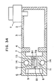
- FIG. 34 and FIG. 35 show a tenth embodiment where generation of uneven plasma can be prevented more effectively.
- FIG. 34 shows the same apparatus as the gas laser apparatus shown in FIG. 7.
- numeral 81 designates an opening edge of a groove 78 to constitute the discharge space 13.
- the opening edge 81 as shown also in FIG. 35 has a smooth arc-shaped surface so that concentration of the electric field to this portion is prevented.
- FIG. 36 and FIG. 37 show an eleventh embodiment as a modification of the tenth embodiment hereinbefore described in FIG. 34 and FIG. 35.
- numeral 91 designates a metallized layer, for example, an aluminium evaporation layer, which is provided integrally with a portion on the dielectrics 12 to cover an opening edge portion 92 of the discharge space as clearly seen in FIG. 37.
- the metallized layer 91 acts to shield the electric field of the microwave so that concentration of the electric field to the opening edge portion 92 is prevented.
- the metallized layer 91 is provided on a portion of the dielectrics 12 to cover the opening edge portion 92 of a groove 93 to form the discharge space 13, the electric field of the microwave can be shielded although it may be concentrated to the opening edge portion 92 without the metallized layer 91. Consequently, the uneven plasma due to the concentration of the electric field can be prevented.
- generation of the uniform microwave discharge plasma 94 in the discharge space 13 is facilitated, the discharge as a whole is made suitable for the laser excitation, the laser resonance mode and the plasma are overlapped well, and the laser output operation with high efficiency and large output becomes possible.
- FIGS. 38 through 41 show still other embodiments.
- numeral 102 designates a laser head section having microwave cavity structure of ridge waveguide type
- numeral 103 designates a magnetron
- numeral 104 designates a waveguide
- numeral 106 designates a microwave coupling window which couples the waveguide 104 to the laser head section 102
- numeral 107 designates a reflection mirror for laser oscillation which is mounted on the laser head section 102.
- numeral 120 designates a cavity wall following the microwave coupling window 106 in the laser head section 102
- numerals 121 and 122 designate ridges provided on center portion of the cavity wall 120 and constituting a part of the microwave circuit
- numeral 123 designates a conductor wall formed on one ridge 121, and in the embodiment a bottom wall surface of a groove 128 provided on an upper surface of the ridge 121 is used as the conductor wall 123.
- Numeral 124 designates dielectrics, for example, by alumina, which is installed opposite to the conductor wall 123 and acts as an incident window of microwave
- numeral 125 designates a discharge space which is formed between the conductor wall 123 and the dielectrics 124 when the dielectrics 124 cover the groove 128 on the upper surface of the ridge 121 and in which the laser gas such as CO2 laser gas is filled.
- the laser head section 102 being the microwave circuit and the waveguide 104 being the microwave transmission path are arranged in parallel in direction along the laser optical axis, and microwave is supplied through the lengthy microwave coupling window 104 provided in the longitudinal direction of the laser head section 102, thereby the strong microwave electromagnetic field can be generated uniformly throughout the whole ridges 121, 122 of the laser head section 102. Consequently, the whole apparatus need not be made large but the long and uniform discharge can be obtained in the laser optical axis and optimum state for the whole discharge and laser excitation is realized.
- FIG. 40 shows a thirteenth embodiment as a modification of the above-mentioned embodiment.
- the waveguide as the microwave transmission path is made a ridge waveguide 104A.
- the microwave transmission path can be miniaturized and the whole configuration of the gas laser apparatus is suppressed to small size and the installation occupied space can be reduced.
- FIG. 41 shows further a fourteenth embodiment of the invention.
- a delay waveguide 104B being a delay transmission path is used as a waveguide, and a dielectric plate 130 as delay medium is internally installed. That is, wavelength of microwave passing through dielectrics in the microwave circuit is shorter than value in the case of passing through the vacuum.
- wavelength of microwave passing through the microwave transmission path such as an ordinary waveguide is longer than value in the case of passing through the vacuum. Consequently, wavelength in each tube of the waveguide as the microwave transmission path and the microwave circuit is not coincident, thereby it is difficult to perform the long and uniform discharge in the laser optical axis direction stably.
- the microwave transmission path is made a delay waveguide 104B having a dielectric plate 130. Thereby two microwave modes are coincident and the stable and uniform discharge and the laser output operation can be realized.
- the microwave coupling window 106 is of lengthy slit form
- plural holes may be arranged in the laser optical axis direction.
- size of holes is gradually decreased in three directions of the magnetron, that is, if the energy density distribution of the microwave is arbitrarily adjusted, the microwave can be uniformly distributed throughout the whole length of the ridges 121, 122, and uniform discharge in the discharge space 125 can be realized stably, and laser output with high efficiency becomes possible.
- the energy density distribution of the microwave and the impedance matching are adjusted simultaneously by the above-mentioned slit or hole
- element for impedance matching may be separately installed and such slit or hole may be installed in other member except for impedance matching.
- laser gas generating plasma by microwave discharge is filled in the discharge space formed between a conductor wall formed in a part of the microwave circuit and dielectrics installed opposite to the conductor wall, and microwave mode having the electric field component orthogonal to the boundary between the dielectrics and the plasma is formed by the microwave circuit, current penetrating between the dielectrics and the conductor wall can flow substantially uniformly within the plasma, thereby the plasma being uniform in space is generated and the laser output can be obtained at high efficiency and large output.
- the microwave circuit and the microwave transmission path are arranged in parallel in the laser optical axis direction, the long and uniform discharge in the laser optical axis direction becomes possible, and the more stable and uniform plasma can be generated in the discharge space, and further the gas laser apparatus can be miniaturized.
Landscapes
- Physics & Mathematics (AREA)
- Electromagnetism (AREA)
- Engineering & Computer Science (AREA)
- Plasma & Fusion (AREA)
- Optics & Photonics (AREA)
- Chemical & Material Sciences (AREA)
- Analytical Chemistry (AREA)
- Lasers (AREA)
- Spectroscopy & Molecular Physics (AREA)
- Health & Medical Sciences (AREA)
- Toxicology (AREA)
- Plasma Technology (AREA)
Priority Applications (1)
| Application Number | Priority Date | Filing Date | Title |
|---|---|---|---|
| EP95108095A EP0674471B1 (fr) | 1987-01-26 | 1988-01-23 | Appareil laser à plasma |
Applications Claiming Priority (32)
| Application Number | Priority Date | Filing Date | Title |
|---|---|---|---|
| JP15690/87 | 1987-01-26 | ||
| JP62015690A JPH0673319B2 (ja) | 1987-01-26 | 1987-01-26 | プラズマ装置 |
| JP18071/87 | 1987-01-28 | ||
| JP1807187A JPH084165B2 (ja) | 1987-01-28 | 1987-01-28 | 気体レ−ザ装置 |
| JP62195185A JP2583518B2 (ja) | 1987-08-06 | 1987-08-06 | 電源装置 |
| JP195185/87 | 1987-08-06 | ||
| JP62225208A JPS6471096A (en) | 1987-09-10 | 1987-09-10 | Plasma device |
| JP62225211A JP2566585B2 (ja) | 1987-09-10 | 1987-09-10 | 光導波路型気体レーザ装置 |
| JP225209/87 | 1987-09-10 | ||
| JP22521587A JPS6469074A (en) | 1987-09-10 | 1987-09-10 | Gas laser equipment |
| JP22521987A JP2566586B2 (ja) | 1987-09-10 | 1987-09-10 | 気体レーザ装置 |
| JP22522487A JPH07105536B2 (ja) | 1987-09-10 | 1987-09-10 | 気体レーザ装置 |
| JP225211/87 | 1987-09-10 | ||
| JP225220/87 | 1987-09-10 | ||
| JP225205/87 | 1987-09-10 | ||
| JP22522287A JPH07105535B2 (ja) | 1987-09-10 | 1987-09-10 | 気体レーザ装置 |
| JP225206/87 | 1987-09-10 | ||
| JP22522087A JPS6469079A (en) | 1987-09-10 | 1987-09-10 | Gas laser equipment |
| JP225214/87 | 1987-09-10 | ||
| JP225221/87 | 1987-09-10 | ||
| JP225219/87 | 1987-09-10 | ||
| JP225224/87 | 1987-09-10 | ||
| JP22520587A JP2566583B2 (ja) | 1987-09-10 | 1987-09-10 | 炭酸ガスレーザ装置 |
| JP22522187A JPS6469080A (en) | 1987-09-10 | 1987-09-10 | Gas laser equipment |
| JP225208/87 | 1987-09-10 | ||
| JP62225206A JPS6469066A (en) | 1987-09-10 | 1987-09-10 | Gas laser equipment |
| JP62225214A JPS6469073A (en) | 1987-09-10 | 1987-09-10 | Gas laser equipment |
| JP62225209A JP2531526B2 (ja) | 1987-09-10 | 1987-09-10 | 気体レ―ザ装置 |
| JP225215/87 | 1987-09-10 | ||
| JP225222/87 | 1987-09-10 | ||
| JP22520287A JPH0682876B2 (ja) | 1987-09-10 | 1987-09-10 | 気体レーザ装置 |
| JP225202/87 | 1987-09-10 |
Related Child Applications (2)
| Application Number | Title | Priority Date | Filing Date |
|---|---|---|---|
| EP95108095A Division EP0674471B1 (fr) | 1987-01-26 | 1988-01-23 | Appareil laser à plasma |
| EP95108095.1 Division-Into | 1988-01-23 |
Publications (3)
| Publication Number | Publication Date |
|---|---|
| EP0280044A2 true EP0280044A2 (fr) | 1988-08-31 |
| EP0280044A3 EP0280044A3 (fr) | 1991-10-23 |
| EP0280044B1 EP0280044B1 (fr) | 1997-05-07 |
Family
ID=27585655
Family Applications (2)
| Application Number | Title | Priority Date | Filing Date |
|---|---|---|---|
| EP95108095A Expired - Lifetime EP0674471B1 (fr) | 1987-01-26 | 1988-01-23 | Appareil laser à plasma |
| EP88101007A Expired - Lifetime EP0280044B1 (fr) | 1987-01-26 | 1988-01-23 | Appareil à plasma |
Family Applications Before (1)
| Application Number | Title | Priority Date | Filing Date |
|---|---|---|---|
| EP95108095A Expired - Lifetime EP0674471B1 (fr) | 1987-01-26 | 1988-01-23 | Appareil laser à plasma |
Country Status (3)
| Country | Link |
|---|---|
| EP (2) | EP0674471B1 (fr) |
| KR (1) | KR910002239B1 (fr) |
| DE (2) | DE3855896T2 (fr) |
Cited By (12)
| Publication number | Priority date | Publication date | Assignee | Title |
|---|---|---|---|---|
| GB2221081A (en) * | 1988-07-20 | 1990-01-24 | British Aerospace | Gas laser |
| DE3912568A1 (de) * | 1989-04-17 | 1990-10-18 | Siemens Ag | Gas-laser, insbesondere co(pfeil abwaerts)2(pfeil abwaerts)-laser |
| GB2234655A (en) * | 1989-07-07 | 1991-02-06 | Charles * Carter Arthur | Heating by gas ionization |
| EP0412555A1 (fr) * | 1989-08-11 | 1991-02-13 | Mitsubishi Denki Kabushiki Kaisha | Dispositif laser à gaz |
| WO1991005450A1 (fr) * | 1989-10-07 | 1991-04-18 | Fraunhofer-Gesellschaft zur Förderung der angewandten Forschung e.V. | Dispositif d'excitation electrique d'un gaz par micro-ondes |
| DE4008195A1 (de) * | 1990-03-15 | 1991-09-26 | Fraunhofer Ges Forschung | Vorrichtung zur anregung des gases einer gasentladungsstrecke mit mikrowellenenergie |
| WO1993002494A1 (fr) * | 1991-07-16 | 1993-02-04 | Suessmuth Norbert | Laser a gaz, notamment laser au co¿2? |
| EP0514585A3 (en) * | 1991-05-21 | 1993-04-28 | Kabushiki Kaisha Kobe Seiko Sho Also Known As Kobe Steel Ltd. | Charged particle accelerator |
| EP0674369A1 (fr) * | 1994-03-23 | 1995-09-27 | Matsushita Electric Industrial Co., Ltd. | Appareil laser à gaz excité par microondes |
| EP1039595A3 (fr) * | 1999-03-26 | 2003-09-10 | Tadahiro Ohmi | Oscillateur laser à gaz |
| CN112996209A (zh) * | 2021-05-07 | 2021-06-18 | 四川大学 | 一种微波激发常压等离子体射流的结构和阵列结构 |
| CN115052407A (zh) * | 2022-07-18 | 2022-09-13 | 浙江大学湖州研究院 | 一种复合场调制微波冷等离子体射流装置 |
Families Citing this family (2)
| Publication number | Priority date | Publication date | Assignee | Title |
|---|---|---|---|---|
| EP1026796B1 (fr) * | 1999-02-01 | 2005-11-16 | Tadahiro Ohmi | Dispositif laser, appareil d'exposition l'utilisant et méthode de fabrication |
| KR20110088658A (ko) * | 2010-01-29 | 2011-08-04 | (주)에스피에스 | 전자파를 이용한 플라즈마 발생장치 및 이를 위한 도파관 |
Family Cites Families (4)
| Publication number | Priority date | Publication date | Assignee | Title |
|---|---|---|---|---|
| US4169251A (en) | 1978-01-16 | 1979-09-25 | Hughes Aircraft Company | Waveguide gas laser with high frequency transverse discharge excitation |
| US4263534A (en) * | 1980-01-08 | 1981-04-21 | International Business Machines Corporation | Single sided sustain voltage generator |
| JPH06105597B2 (ja) * | 1982-08-30 | 1994-12-21 | 株式会社日立製作所 | マイクロ波プラズマ源 |
| ZA841218B (en) * | 1983-03-08 | 1984-09-26 | Allied Corp | Plasma excitation system |
-
1988
- 1988-01-23 EP EP95108095A patent/EP0674471B1/fr not_active Expired - Lifetime
- 1988-01-23 DE DE3855896T patent/DE3855896T2/de not_active Expired - Fee Related
- 1988-01-23 DE DE3856348T patent/DE3856348T2/de not_active Expired - Fee Related
- 1988-01-23 EP EP88101007A patent/EP0280044B1/fr not_active Expired - Lifetime
- 1988-01-25 KR KR1019880000551A patent/KR910002239B1/ko not_active Expired
Cited By (20)
| Publication number | Priority date | Publication date | Assignee | Title |
|---|---|---|---|---|
| US5007064A (en) * | 1988-07-20 | 1991-04-09 | British Aerospace Plc | Gas laser |
| GB2221081B (en) * | 1988-07-20 | 1992-09-16 | British Aerospace | Gas laser |
| GB2221081A (en) * | 1988-07-20 | 1990-01-24 | British Aerospace | Gas laser |
| DE3912568A1 (de) * | 1989-04-17 | 1990-10-18 | Siemens Ag | Gas-laser, insbesondere co(pfeil abwaerts)2(pfeil abwaerts)-laser |
| WO1990013160A1 (fr) * | 1989-04-17 | 1990-11-01 | Siemens Aktiengesellschaft | Laser a gas, notamment laser au co¿2? |
| GB2234655A (en) * | 1989-07-07 | 1991-02-06 | Charles * Carter Arthur | Heating by gas ionization |
| EP0412555A1 (fr) * | 1989-08-11 | 1991-02-13 | Mitsubishi Denki Kabushiki Kaisha | Dispositif laser à gaz |
| WO1991005450A1 (fr) * | 1989-10-07 | 1991-04-18 | Fraunhofer-Gesellschaft zur Förderung der angewandten Forschung e.V. | Dispositif d'excitation electrique d'un gaz par micro-ondes |
| DE3933619A1 (de) * | 1989-10-07 | 1991-04-18 | Fraunhofer Ges Forschung | Vorrichtung zur elektrischen anregung eines gases mit mikrowellen |
| DE4008195A1 (de) * | 1990-03-15 | 1991-09-26 | Fraunhofer Ges Forschung | Vorrichtung zur anregung des gases einer gasentladungsstrecke mit mikrowellenenergie |
| US5280252A (en) * | 1991-05-21 | 1994-01-18 | Kabushiki Kaisha Kobe Seiko Sho | Charged particle accelerator |
| EP0514585A3 (en) * | 1991-05-21 | 1993-04-28 | Kabushiki Kaisha Kobe Seiko Sho Also Known As Kobe Steel Ltd. | Charged particle accelerator |
| WO1993002494A1 (fr) * | 1991-07-16 | 1993-02-04 | Suessmuth Norbert | Laser a gaz, notamment laser au co¿2? |
| US5400357A (en) * | 1991-07-16 | 1995-03-21 | Suessmuth; Norbert | Gas laser in particular CO2 laser |
| EP0674369A1 (fr) * | 1994-03-23 | 1995-09-27 | Matsushita Electric Industrial Co., Ltd. | Appareil laser à gaz excité par microondes |
| US5606571A (en) * | 1994-03-23 | 1997-02-25 | Matsushita Electric Industrial Co., Ltd. | Microwave powered gas laser apparatus |
| EP1039595A3 (fr) * | 1999-03-26 | 2003-09-10 | Tadahiro Ohmi | Oscillateur laser à gaz |
| US6801554B1 (en) | 1999-03-26 | 2004-10-05 | Canon Kabushiki Kaisha | Laser oscillating apparatus, exposure apparatus, and device fabrication method |
| CN112996209A (zh) * | 2021-05-07 | 2021-06-18 | 四川大学 | 一种微波激发常压等离子体射流的结构和阵列结构 |
| CN115052407A (zh) * | 2022-07-18 | 2022-09-13 | 浙江大学湖州研究院 | 一种复合场调制微波冷等离子体射流装置 |
Also Published As
| Publication number | Publication date |
|---|---|
| KR910002239B1 (ko) | 1991-04-08 |
| EP0674471B1 (fr) | 1999-07-07 |
| KR880009461A (ko) | 1988-09-15 |
| EP0280044A3 (fr) | 1991-10-23 |
| EP0674471A1 (fr) | 1995-09-27 |
| EP0280044B1 (fr) | 1997-05-07 |
| DE3855896T2 (de) | 1998-01-02 |
| DE3856348D1 (de) | 1999-08-12 |
| DE3855896D1 (de) | 1997-06-12 |
| DE3856348T2 (de) | 1999-11-25 |
Similar Documents
| Publication | Publication Date | Title |
|---|---|---|
| US4890294A (en) | Plasma apparatus | |
| EP0280044B1 (fr) | Appareil à plasma | |
| US4169251A (en) | Waveguide gas laser with high frequency transverse discharge excitation | |
| US6922021B2 (en) | Microwave energized plasma lamp with solid dielectric waveguide | |
| CA2087562C (fr) | Appareil a laser | |
| US7453918B2 (en) | Pulsed RF high pressure CO2 lasers | |
| KR20010012603A (ko) | 일체식 전치 전리장치를 갖는 소형의 엑시머 레이저 절연체 | |
| US3431511A (en) | Optical maser apparatus with pump trigger | |
| US4247829A (en) | Silent discharge type gas laser device | |
| US6298806B1 (en) | Device for exciting a gas by a surface wave plasma | |
| US5239551A (en) | Microwave-driven UV solid-state laser | |
| US4710941A (en) | Perforated electrodes for efficient gas transfer in CW CO2 waveguide lasers | |
| US6711201B2 (en) | Truncated ridge waveguide for all-metal gas laser excitation | |
| JPH0432281A (ja) | マイクロ波励起気体レーザ装置 | |
| US6442185B1 (en) | All-metal, DC excited laser with RF pre-ionization | |
| Huchital et al. | Pumping of Nd: YAG with electrodeless arc lamps | |
| JP2566583B2 (ja) | 炭酸ガスレーザ装置 | |
| JPH0724315B2 (ja) | 気体レーザ装置 | |
| JPH0673319B2 (ja) | プラズマ装置 | |
| US5400357A (en) | Gas laser in particular CO2 laser | |
| JP2566585B2 (ja) | 光導波路型気体レーザ装置 | |
| RU753325C (ru) | Газовый лазер | |
| JPH07105536B2 (ja) | 気体レーザ装置 | |
| US3970961A (en) | Thermionic cathode transverse-discharge gas laser tube | |
| JPH07105535B2 (ja) | 気体レーザ装置 |
Legal Events
| Date | Code | Title | Description |
|---|---|---|---|
| PUAI | Public reference made under article 153(3) epc to a published international application that has entered the european phase |
Free format text: ORIGINAL CODE: 0009012 |
|
| AK | Designated contracting states |
Kind code of ref document: A2 Designated state(s): DE FR GB |
|
| PUAL | Search report despatched |
Free format text: ORIGINAL CODE: 0009013 |
|
| AK | Designated contracting states |
Kind code of ref document: A3 Designated state(s): DE FR GB |
|
| RHK1 | Main classification (correction) |
Ipc: H05H 1/46 |
|
| 17P | Request for examination filed |
Effective date: 19911205 |
|
| 17Q | First examination report despatched |
Effective date: 19940517 |
|
| GRAG | Despatch of communication of intention to grant |
Free format text: ORIGINAL CODE: EPIDOS AGRA |
|
| GRAH | Despatch of communication of intention to grant a patent |
Free format text: ORIGINAL CODE: EPIDOS IGRA |
|
| GRAH | Despatch of communication of intention to grant a patent |
Free format text: ORIGINAL CODE: EPIDOS IGRA |
|
| GRAA | (expected) grant |
Free format text: ORIGINAL CODE: 0009210 |
|
| AK | Designated contracting states |
Kind code of ref document: B1 Designated state(s): DE FR GB |
|
| XX | Miscellaneous (additional remarks) |
Free format text: TEILANMELDUNG 95108095.1 EINGEREICHT AM 23/01/88. |
|
| REF | Corresponds to: |
Ref document number: 3855896 Country of ref document: DE Date of ref document: 19970612 |
|
| ET | Fr: translation filed | ||
| PLBE | No opposition filed within time limit |
Free format text: ORIGINAL CODE: 0009261 |
|
| STAA | Information on the status of an ep patent application or granted ep patent |
Free format text: STATUS: NO OPPOSITION FILED WITHIN TIME LIMIT |
|
| 26N | No opposition filed | ||
| REG | Reference to a national code |
Ref country code: GB Ref legal event code: 746 Effective date: 20000126 |
|
| REG | Reference to a national code |
Ref country code: GB Ref legal event code: IF02 |
|
| PGFP | Annual fee paid to national office [announced via postgrant information from national office to epo] |
Ref country code: FR Payment date: 20030110 Year of fee payment: 16 |
|
| PGFP | Annual fee paid to national office [announced via postgrant information from national office to epo] |
Ref country code: DE Payment date: 20030130 Year of fee payment: 16 |
|
| PG25 | Lapsed in a contracting state [announced via postgrant information from national office to epo] |
Ref country code: DE Free format text: LAPSE BECAUSE OF NON-PAYMENT OF DUE FEES Effective date: 20040803 |
|
| PG25 | Lapsed in a contracting state [announced via postgrant information from national office to epo] |
Ref country code: FR Free format text: LAPSE BECAUSE OF NON-PAYMENT OF DUE FEES Effective date: 20040930 |
|
| REG | Reference to a national code |
Ref country code: FR Ref legal event code: ST |
|
| PGFP | Annual fee paid to national office [announced via postgrant information from national office to epo] |
Ref country code: GB Payment date: 20070117 Year of fee payment: 20 |
|
| REG | Reference to a national code |
Ref country code: GB Ref legal event code: PE20 |
|
| PG25 | Lapsed in a contracting state [announced via postgrant information from national office to epo] |
Ref country code: GB Free format text: LAPSE BECAUSE OF EXPIRATION OF PROTECTION Effective date: 20080122 |