EP0280073A2 - Support de circuit comprenant des éléments résistifs - Google Patents
Support de circuit comprenant des éléments résistifs Download PDFInfo
- Publication number
- EP0280073A2 EP0280073A2 EP88101464A EP88101464A EP0280073A2 EP 0280073 A2 EP0280073 A2 EP 0280073A2 EP 88101464 A EP88101464 A EP 88101464A EP 88101464 A EP88101464 A EP 88101464A EP 0280073 A2 EP0280073 A2 EP 0280073A2
- Authority
- EP
- European Patent Office
- Prior art keywords
- electrode
- resistance film
- conductor
- resistance
- resistor element
- Prior art date
- Legal status (The legal status is an assumption and is not a legal conclusion. Google has not performed a legal analysis and makes no representation as to the accuracy of the status listed.)
- Withdrawn
Links
Images

Classifications
-
- H—ELECTRICITY
- H01—ELECTRIC ELEMENTS
- H01C—RESISTORS
- H01C1/00—Details
- H01C1/14—Terminals or tapping points specially adapted for resistors; Arrangements of terminals or tapping points on resistors
- H01C1/142—Terminals or tapping points specially adapted for resistors; Arrangements of terminals or tapping points on resistors the terminals or tapping points being coated on the resistive element
-
- H—ELECTRICITY
- H05—ELECTRIC TECHNIQUES NOT OTHERWISE PROVIDED FOR
- H05K—PRINTED CIRCUITS; CASINGS OR CONSTRUCTIONAL DETAILS OF ELECTRIC APPARATUS; MANUFACTURE OF ASSEMBLAGES OF ELECTRICAL COMPONENTS
- H05K1/00—Printed circuits
- H05K1/16—Printed circuits incorporating printed electric components, e.g. printed resistors, capacitors or inductors
- H05K1/167—Printed circuits incorporating printed electric components, e.g. printed resistors, capacitors or inductors incorporating printed resistors
-
- H—ELECTRICITY
- H05—ELECTRIC TECHNIQUES NOT OTHERWISE PROVIDED FOR
- H05K—PRINTED CIRCUITS; CASINGS OR CONSTRUCTIONAL DETAILS OF ELECTRIC APPARATUS; MANUFACTURE OF ASSEMBLAGES OF ELECTRICAL COMPONENTS
- H05K1/00—Printed circuits
- H05K1/02—Details
- H05K1/11—Printed elements for providing electric connections to or between printed circuits
- H05K1/115—Via connections; Lands around holes or via connections
- H05K1/116—Lands, clearance holes or other lay-out details concerning the surrounding of a via
-
- H—ELECTRICITY
- H05—ELECTRIC TECHNIQUES NOT OTHERWISE PROVIDED FOR
- H05K—PRINTED CIRCUITS; CASINGS OR CONSTRUCTIONAL DETAILS OF ELECTRIC APPARATUS; MANUFACTURE OF ASSEMBLAGES OF ELECTRICAL COMPONENTS
- H05K2201/00—Indexing scheme relating to printed circuits covered by H05K1/00
- H05K2201/03—Conductive materials
- H05K2201/0302—Properties and characteristics in general
- H05K2201/0317—Thin film conductor layer; Thin film passive component
-
- H—ELECTRICITY
- H05—ELECTRIC TECHNIQUES NOT OTHERWISE PROVIDED FOR
- H05K—PRINTED CIRCUITS; CASINGS OR CONSTRUCTIONAL DETAILS OF ELECTRIC APPARATUS; MANUFACTURE OF ASSEMBLAGES OF ELECTRICAL COMPONENTS
- H05K2203/00—Indexing scheme relating to apparatus or processes for manufacturing printed circuits covered by H05K3/00
- H05K2203/14—Related to the order of processing steps
- H05K2203/1453—Applying the circuit pattern before another process, e.g. before filling of vias with conductive paste, before making printed resistors
-
- H—ELECTRICITY
- H05—ELECTRIC TECHNIQUES NOT OTHERWISE PROVIDED FOR
- H05K—PRINTED CIRCUITS; CASINGS OR CONSTRUCTIONAL DETAILS OF ELECTRIC APPARATUS; MANUFACTURE OF ASSEMBLAGES OF ELECTRICAL COMPONENTS
- H05K3/00—Apparatus or processes for manufacturing printed circuits
- H05K3/22—Secondary treatment of printed circuits
- H05K3/24—Reinforcing of the conductive pattern
- H05K3/244—Finish plating of conductors, especially of copper conductors, e.g. for pads or lands
Definitions
- the present invention relates to a circuit substrate for packaging electronic components and, more particularly, to a structure of a resistor element to be formed on or in a substrate.
- the electrode is formed by arranging a conductor in contact with at least one of upper and lower sides at each of the two ends of a square resistance film.
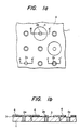
- the electrode structure as disclosed in Japanese Patent Laid-Open No. 136391/1985 will be described in summary with reference to Fig. 1a.
- a substrate 1 is formed in its surface with a electrode conductor (e.g., a circular through-hole conductor extending through the back of the substrate 1) 2b.
- This circular electrode conductor 2b is concentrically surrounded by a film resistor 3 which forms part of a resistance layer on the substrate 1.
- Another electrode conductor 4 is formed on the outer circumference of the film resistor 3.
- the resistor 3 is once formed on the substrate 1 by the sputtering process. Then, the conductor layer is formed on the resistor 3 and partially removed by the etching process or the like to shape the resistor 3 interposed between the two electrode conductors. Specifically, the resistor 3 is interposed between one electrode conductor 2b and the other electrode conductor 4, thus constituting one resistor element.
- this resistor element having the structure of the prior art is still insufficient for the recent requirements such as high integration, size reduction or high precision (or accuracy) of the set values, e.g., the resistance of a circuit element.
- the prior art took no consideration from the point of forming a resistor element of high precision resistance but underwent the trimming process for partially removing the resistance film forming part of the resistor element to control resistance. The trimming process incurs more or less error in the area of the resistance film so that the distribution of the current flowing through the resistance film becomes uneven.
- An object of the present invention is to provide a circuit substrate including a resistor element having a high precision resistance while eliminating the trimming process of the prior art.
- a circuit substrate which comprises: a first electrode conductor made of a relatively thick wiring conductor and overlapping partially the upper or lower side of a resistance film; and a second electrode conductor made of a relatively thin conductor and covering the overlapping portion of said resistance film and said first electrode conductor and at least a portion of the exposed portion (of said first electrode conductor) continuing from said overlapping portion.
- One of the major factors exerting influences upon the precision of the resistance owned by the resistor element is the shape and dimensional precisions of conductors forming the electrodes of the resistor element. If the area to be occupied by the resistor element is especially restricted for high density wiring, the shape and dimensional precisions of the conductors forming the electrodes constitute major factor for the fluctuations of the resistance.
- the circuit substrate of the present invention comprises a first electrode formed out of a thick wiring conductor in advance on upper or lower side of a resistance film.
- a second electrode of a thin conductor is formed to have a larger area overlapping on the resistance film than that of the thick conductor.
- the first electrode of the resistor element is formed out of the relatively thick wiring conductor, and the resistance film is connected directly with the thick electrode and is in sufficient contact with the resistance film through the second electrode conductor.
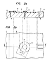
- Fig. 2a is a section showing the circuit substrate which has a resistor element on the surface of a substrate 11.
- Numeral 13 designates a thick conductor which forms a first electrode of the resistor element and is connected with a through hole 15.
- Numeral 14 designates a thin conductor which forms a second electrode on a resistance film 12.
- Fig. 2b is a top plan view showing the construction of the circuit substrate of the present invention and has its section taken along dotted line and presented in Fig. 2a.
- the thick conductor layer 13 is formed all over the surface of the substrate 11 which is made of an inorganic material such as ceramics or an organic material such as resins.
- the conductor layer is etched by the photoetching process or the like except the portion corresponding to the through-hole 15 and another desired electrode portion.
- the wiring electrode 13 connected with the portion of the through hole 15 and the first electrode serving as a connecting conductor of the resistor element are formed.
- the thickness of the first electrode conductor 13 is set at a lower level than the wiring resistance required of the circuit substrate to be fabricated.
- the resistance film 12 is formed all over the surface by the thin-film process such as the sintering, evaporating or sputtering of thick paste.
- the resistance film 12 is photoetched except the region for the arrangement of the resistance element.
- the resistance film 12 is made to overlap the conductor partially.
- the conductor 14 thinner than the conductor 13 is layered all over the surface of the substrate having the first electrode and the resistance film and is as shown by Fig.
- the resistance of the resistor element is determined under the sheet resistance of the film 12 exclusively by the shape and size of the conductor 14, i.e., by the sizes of the internal diameter a and external diameter b of the annulus shown in Fig. 2b in the present embodiment.
- the resistance film is assumed to have a constant thickness.
- the shape and size will fluctuate depending upon the under- or overetching due to the fluctuations of the working conditions.
- the time period required for the etching process in the shorter for the thinner conductors.
- the thin conductors can afford high precision shape and size without being highly influenced by the fluctuations of the etching conditions. This makes it possible to make the conductor 14 thin to such an extent (e.g. , 1 microns) that the resistance of the second electrode itself is not high.
- the resistance is controlled by using a thin conductor so that a resistance film having a high precision resistance can be formed. Since, moreover, a first thick electrode is used as one for wiring the resistance film, the resistor element can be connected with another electric circuit without increasing the wiring resistance.
- circuit substrate having a square resistor element Another embodiment of the circuit substrate having a square resistor element will be described in the following with reference to Figs. 3a and 3b.
- Fig. 3a is a section showing a circuit substrate having a resistor element formed out of a square resistance film.
- the thick conductor 13 is a first electrode formed on the resistance film 12 and provides a wiring for connecting the resistor element with another electric circuit.
- the thin conductor 14 forms a second electrode which is constructed to partially overlap the conductor 13 and the resistance film 12.
- Fig. 3b is a top plan view showing the present circuit substrate, and Fig. 3a is a section taken along line A - A ⁇ of Fig. 3b.
- the present circuit substrate can be fabricated similarly to the embodiment of Figs. 2a and 2b except that the forming order is the resistance film 12, the conductor 13 and the conductor 14.
- the thin conductor 14 forming the second electrode overlaps the resistance film 12 with a wider area than that of the thick conductor forming the first electrode.
- the resistance owned by the resistor element is determined by the size a and the width W of the square resistance film, as shown in Fig. 3b. Because the conductor 14 is thin, moreover, the conductor 14 can be worked in high precision with respect to the size a. Because the thickness of the resistance film is usually as small as about 0.1 microns, still moreover, the resistance film can also be worked in high precision. Thus, it is possible to form a resistor element having a high precision resistance. Because the thick conductor forms both the first electrode and the wiring, furthermore, the resistor element can be connected with another electric circuit without increasing the wiring resistance.
- the resistor element having a high precision resistance can be formed while eliminating the trimming process of the prior art for controlling the resistance.
- the elimination of the trimming process is highly effective in shortening the process for fabricating the substrate having the resistor element.
- the embodiments of the present invention thus far described are exemplified by a single substrate.
- the structure of the present invention can naturally be applied to the internal wiring layer of the structure having a multilayer interconnection circuit.
Landscapes
- Engineering & Computer Science (AREA)
- Microelectronics & Electronic Packaging (AREA)
- Parts Printed On Printed Circuit Boards (AREA)
- Non-Adjustable Resistors (AREA)
- Production Of Multi-Layered Print Wiring Board (AREA)
Applications Claiming Priority (2)
| Application Number | Priority Date | Filing Date | Title |
|---|---|---|---|
| JP37997/87 | 1987-02-23 | ||
| JP3799787A JPS63205991A (ja) | 1987-02-23 | 1987-02-23 | 回路基板 |
Publications (2)
| Publication Number | Publication Date |
|---|---|
| EP0280073A2 true EP0280073A2 (fr) | 1988-08-31 |
| EP0280073A3 EP0280073A3 (fr) | 1990-01-10 |
Family
ID=12513216
Family Applications (1)
| Application Number | Title | Priority Date | Filing Date |
|---|---|---|---|
| EP88101464A Withdrawn EP0280073A3 (fr) | 1987-02-23 | 1988-02-02 | Support de circuit comprenant des éléments résistifs |
Country Status (2)
| Country | Link |
|---|---|
| EP (1) | EP0280073A3 (fr) |
| JP (1) | JPS63205991A (fr) |
Cited By (1)
| Publication number | Priority date | Publication date | Assignee | Title |
|---|---|---|---|---|
| US5557251A (en) * | 1993-03-29 | 1996-09-17 | Murata Manufacturing Co., Ltd. | Thermistor with electrodes for preventing inter-electrode migration |
Family Cites Families (1)
| Publication number | Priority date | Publication date | Assignee | Title |
|---|---|---|---|---|
| JPS5535843B2 (fr) * | 1972-12-28 | 1980-09-17 |
-
1987
- 1987-02-23 JP JP3799787A patent/JPS63205991A/ja active Pending
-
1988
- 1988-02-02 EP EP88101464A patent/EP0280073A3/fr not_active Withdrawn
Cited By (1)
| Publication number | Priority date | Publication date | Assignee | Title |
|---|---|---|---|---|
| US5557251A (en) * | 1993-03-29 | 1996-09-17 | Murata Manufacturing Co., Ltd. | Thermistor with electrodes for preventing inter-electrode migration |
Also Published As
| Publication number | Publication date |
|---|---|
| EP0280073A3 (fr) | 1990-01-10 |
| JPS63205991A (ja) | 1988-08-25 |
Similar Documents
| Publication | Publication Date | Title |
|---|---|---|
| US6943662B2 (en) | Chip resistor | |
| US6005474A (en) | Chip network resistor and method for manufacturing same | |
| US5539227A (en) | Multi-layer wiring | |
| US6194248B1 (en) | Chip electronic part | |
| US4725925A (en) | Circuit board | |
| US5699224A (en) | Thick-film capacitor and chip-type composite electronic component utilizing the same | |
| US5973390A (en) | Chip electronic part | |
| US5790385A (en) | One-chip electronic composite component | |
| KR100206621B1 (ko) | 칩형 후막 콘덴서 및 그의 제조 방법 | |
| EP0441374A1 (fr) | Elément semiconducteur pourvu de condensateurs | |
| JP2739453B2 (ja) | ヒューズ機能付コンデンサ、及びその製造方法 | |
| US7105911B2 (en) | Multilayer electronic substrate, and the method of manufacturing multilayer electronic substrate | |
| JPS63205991A (ja) | 回路基板 | |
| JPS628040B2 (fr) | ||
| JPS61134053A (ja) | 半導体集積回路装置 | |
| JPH0138924Y2 (fr) | ||
| JP2000299342A (ja) | バンプ電極及びその製造方法 | |
| JPS6336641Y2 (fr) | ||
| JPH027482Y2 (fr) | ||
| JPH08255969A (ja) | プリント基板装置 | |
| JPH09246093A (ja) | 厚膜コンデンサ | |
| JPS6041252A (ja) | 混成集積回路の製造方法 | |
| JPS6181680A (ja) | 厚膜パタ−ンの形成方法 | |
| JPH0557740B2 (fr) | ||
| JPH0339260A (ja) | サーマルヘッド及びその製造方法 |
Legal Events
| Date | Code | Title | Description |
|---|---|---|---|
| PUAI | Public reference made under article 153(3) epc to a published international application that has entered the european phase |
Free format text: ORIGINAL CODE: 0009012 |
|
| AK | Designated contracting states |
Kind code of ref document: A2 Designated state(s): DE FR GB |
|
| PUAL | Search report despatched |
Free format text: ORIGINAL CODE: 0009013 |
|
| AK | Designated contracting states |
Kind code of ref document: A3 Designated state(s): DE FR GB |
|
| 17P | Request for examination filed |
Effective date: 19900112 |
|
| 17Q | First examination report despatched |
Effective date: 19910506 |
|
| STAA | Information on the status of an ep patent application or granted ep patent |
Free format text: STATUS: THE APPLICATION HAS BEEN WITHDRAWN |
|
| RAP1 | Party data changed (applicant data changed or rights of an application transferred) |
Owner name: HITACHI, LTD. Owner name: HITACHI MICROCOMPUTER SYSTEM LTD. |
|
| 18W | Application withdrawn |
Withdrawal date: 19910722 |
|
| R18W | Application withdrawn (corrected) |
Effective date: 19910722 |