EP0280531A2 - Optischer Datenaufzeichnungsträger - Google Patents
Optischer Datenaufzeichnungsträger Download PDFInfo
- Publication number
- EP0280531A2 EP0280531A2 EP88301586A EP88301586A EP0280531A2 EP 0280531 A2 EP0280531 A2 EP 0280531A2 EP 88301586 A EP88301586 A EP 88301586A EP 88301586 A EP88301586 A EP 88301586A EP 0280531 A2 EP0280531 A2 EP 0280531A2
- Authority
- EP
- European Patent Office
- Prior art keywords
- layer
- information recording
- optical
- optical information
- recording carrier
- Prior art date
- Legal status (The legal status is an assumption and is not a legal conclusion. Google has not performed a legal analysis and makes no representation as to the accuracy of the status listed.)
- Granted
Links
- 230000003287 optical effect Effects 0.000 title claims abstract description 125
- 239000010410 layer Substances 0.000 claims abstract description 133
- 239000000758 substrate Substances 0.000 claims abstract description 57
- 239000007888 film coating Substances 0.000 claims abstract description 34
- 238000009501 film coating Methods 0.000 claims abstract description 34
- 229920005989 resin Polymers 0.000 claims description 25
- 239000011347 resin Substances 0.000 claims description 25
- 230000008859 change Effects 0.000 claims description 13
- 230000015572 biosynthetic process Effects 0.000 claims description 10
- 229920001169 thermoplastic Polymers 0.000 claims description 8
- 239000004416 thermosoftening plastic Substances 0.000 claims description 8
- 239000012790 adhesive layer Substances 0.000 claims description 7
- 229920000139 polyethylene terephthalate Polymers 0.000 claims description 7
- 239000005020 polyethylene terephthalate Substances 0.000 claims description 7
- 239000011342 resin composition Substances 0.000 claims description 5
- 229920005992 thermoplastic resin Polymers 0.000 claims description 5
- 229920000728 polyester Polymers 0.000 claims description 4
- 239000000853 adhesive Substances 0.000 description 23
- 230000001070 adhesive effect Effects 0.000 description 23
- 239000000975 dye Substances 0.000 description 22
- 239000010408 film Substances 0.000 description 20
- 238000000034 method Methods 0.000 description 17
- 230000035945 sensitivity Effects 0.000 description 17
- 230000001681 protective effect Effects 0.000 description 14
- 239000010409 thin film Substances 0.000 description 14
- 238000005538 encapsulation Methods 0.000 description 13
- 239000000463 material Substances 0.000 description 12
- 229920000515 polycarbonate Polymers 0.000 description 11
- 239000004417 polycarbonate Substances 0.000 description 11
- 238000000576 coating method Methods 0.000 description 9
- -1 polyethylene Polymers 0.000 description 9
- VYPSYNLAJGMNEJ-UHFFFAOYSA-N Silicium dioxide Chemical compound O=[Si]=O VYPSYNLAJGMNEJ-UHFFFAOYSA-N 0.000 description 8
- 239000011248 coating agent Substances 0.000 description 8
- 239000003446 ligand Substances 0.000 description 8
- 239000003795 chemical substances by application Substances 0.000 description 6
- 230000000052 comparative effect Effects 0.000 description 6
- 230000006866 deterioration Effects 0.000 description 6
- 239000005038 ethylene vinyl acetate Substances 0.000 description 6
- 229910052751 metal Inorganic materials 0.000 description 6
- 239000002184 metal Substances 0.000 description 6
- 239000000203 mixture Substances 0.000 description 6
- 229920001200 poly(ethylene-vinyl acetate) Polymers 0.000 description 6
- 238000010791 quenching Methods 0.000 description 6
- 230000000171 quenching effect Effects 0.000 description 6
- 238000002834 transmittance Methods 0.000 description 6
- NIXOWILDQLNWCW-UHFFFAOYSA-N acrylic acid group Chemical group C(C=C)(=O)O NIXOWILDQLNWCW-UHFFFAOYSA-N 0.000 description 5
- 150000001875 compounds Chemical class 0.000 description 5
- 229920001577 copolymer Polymers 0.000 description 5
- 230000000694 effects Effects 0.000 description 5
- 238000002844 melting Methods 0.000 description 5
- 230000008018 melting Effects 0.000 description 5
- 238000004528 spin coating Methods 0.000 description 5
- 229920003048 styrene butadiene rubber Polymers 0.000 description 5
- DQXBYHZEEUGOBF-UHFFFAOYSA-N but-3-enoic acid;ethene Chemical compound C=C.OC(=O)CC=C DQXBYHZEEUGOBF-UHFFFAOYSA-N 0.000 description 4
- 238000006243 chemical reaction Methods 0.000 description 4
- 238000001514 detection method Methods 0.000 description 4
- 239000000123 paper Substances 0.000 description 4
- 229920000573 polyethylene Polymers 0.000 description 4
- 150000003839 salts Chemical class 0.000 description 4
- 239000004065 semiconductor Substances 0.000 description 4
- 239000000377 silicon dioxide Substances 0.000 description 4
- 239000011135 tin Substances 0.000 description 4
- SCYULBFZEHDVBN-UHFFFAOYSA-N 1,1-Dichloroethane Chemical compound CC(Cl)Cl SCYULBFZEHDVBN-UHFFFAOYSA-N 0.000 description 3
- NIXOWILDQLNWCW-UHFFFAOYSA-M Acrylate Chemical compound [O-]C(=O)C=C NIXOWILDQLNWCW-UHFFFAOYSA-M 0.000 description 3
- YMWUJEATGCHHMB-UHFFFAOYSA-N Dichloromethane Chemical compound ClCCl YMWUJEATGCHHMB-UHFFFAOYSA-N 0.000 description 3
- 239000004593 Epoxy Substances 0.000 description 3
- WSFSSNUMVMOOMR-UHFFFAOYSA-N Formaldehyde Chemical compound O=C WSFSSNUMVMOOMR-UHFFFAOYSA-N 0.000 description 3
- 239000004952 Polyamide Substances 0.000 description 3
- 239000004698 Polyethylene Substances 0.000 description 3
- 239000004642 Polyimide Substances 0.000 description 3
- 239000001913 cellulose Substances 0.000 description 3
- 229920002678 cellulose Polymers 0.000 description 3
- 239000010949 copper Substances 0.000 description 3
- 238000000465 moulding Methods 0.000 description 3
- 239000011368 organic material Substances 0.000 description 3
- 229920002647 polyamide Polymers 0.000 description 3
- 229920006267 polyester film Polymers 0.000 description 3
- 229920001721 polyimide Polymers 0.000 description 3
- KCTAWXVAICEBSD-UHFFFAOYSA-N prop-2-enoyloxy prop-2-eneperoxoate Chemical compound C=CC(=O)OOOC(=O)C=C KCTAWXVAICEBSD-UHFFFAOYSA-N 0.000 description 3
- 239000000243 solution Substances 0.000 description 3
- 238000000859 sublimation Methods 0.000 description 3
- 230000008022 sublimation Effects 0.000 description 3
- MSAHTMIQULFMRG-UHFFFAOYSA-N 1,2-diphenyl-2-propan-2-yloxyethanone Chemical compound C=1C=CC=CC=1C(OC(C)C)C(=O)C1=CC=CC=C1 MSAHTMIQULFMRG-UHFFFAOYSA-N 0.000 description 2
- SMZOUWXMTYCWNB-UHFFFAOYSA-N 2-(2-methoxy-5-methylphenyl)ethanamine Chemical compound COC1=CC=C(C)C=C1CCN SMZOUWXMTYCWNB-UHFFFAOYSA-N 0.000 description 2
- 229920000178 Acrylic resin Polymers 0.000 description 2
- 239000004925 Acrylic resin Substances 0.000 description 2
- QGZKDVFQNNGYKY-UHFFFAOYSA-N Ammonia Chemical compound N QGZKDVFQNNGYKY-UHFFFAOYSA-N 0.000 description 2
- 229930185605 Bisphenol Natural products 0.000 description 2
- XEEYBQQBJWHFJM-UHFFFAOYSA-N Iron Chemical compound [Fe] XEEYBQQBJWHFJM-UHFFFAOYSA-N 0.000 description 2
- 239000004419 Panlite Substances 0.000 description 2
- XYFCBTPGUUZFHI-UHFFFAOYSA-N Phosphine Chemical compound P XYFCBTPGUUZFHI-UHFFFAOYSA-N 0.000 description 2
- 229930182556 Polyacetal Natural products 0.000 description 2
- 239000004793 Polystyrene Substances 0.000 description 2
- 239000002174 Styrene-butadiene Substances 0.000 description 2
- XTXRWKRVRITETP-UHFFFAOYSA-N Vinyl acetate Chemical compound CC(=O)OC=C XTXRWKRVRITETP-UHFFFAOYSA-N 0.000 description 2
- 229920002433 Vinyl chloride-vinyl acetate copolymer Polymers 0.000 description 2
- 239000006096 absorbing agent Substances 0.000 description 2
- 230000001133 acceleration Effects 0.000 description 2
- QVGXLLKOCUKJST-UHFFFAOYSA-N atomic oxygen Chemical class [O] QVGXLLKOCUKJST-UHFFFAOYSA-N 0.000 description 2
- 230000001588 bifunctional effect Effects 0.000 description 2
- IISBACLAFKSPIT-UHFFFAOYSA-N bisphenol A Chemical compound C=1C=C(O)C=CC=1C(C)(C)C1=CC=C(O)C=C1 IISBACLAFKSPIT-UHFFFAOYSA-N 0.000 description 2
- 229910052802 copper Inorganic materials 0.000 description 2
- 238000001035 drying Methods 0.000 description 2
- 239000000839 emulsion Substances 0.000 description 2
- 229920006228 ethylene acrylate copolymer Polymers 0.000 description 2
- 239000007789 gas Substances 0.000 description 2
- 230000006872 improvement Effects 0.000 description 2
- 230000005764 inhibitory process Effects 0.000 description 2
- 238000001746 injection moulding Methods 0.000 description 2
- 230000031700 light absorption Effects 0.000 description 2
- 239000002923 metal particle Substances 0.000 description 2
- 150000002739 metals Chemical class 0.000 description 2
- YDKNBNOOCSNPNS-UHFFFAOYSA-N methyl 1,3-benzoxazole-2-carboxylate Chemical compound C1=CC=C2OC(C(=O)OC)=NC2=C1 YDKNBNOOCSNPNS-UHFFFAOYSA-N 0.000 description 2
- 239000000178 monomer Substances 0.000 description 2
- 239000001301 oxygen Substances 0.000 description 2
- 229910052760 oxygen Inorganic materials 0.000 description 2
- 229920002492 poly(sulfone) Polymers 0.000 description 2
- 229920006122 polyamide resin Polymers 0.000 description 2
- 229920005668 polycarbonate resin Polymers 0.000 description 2
- 239000004431 polycarbonate resin Substances 0.000 description 2
- 229920001225 polyester resin Polymers 0.000 description 2
- 239000004645 polyester resin Substances 0.000 description 2
- 238000006116 polymerization reaction Methods 0.000 description 2
- 229920005672 polyolefin resin Polymers 0.000 description 2
- 229920006324 polyoxymethylene Polymers 0.000 description 2
- 229920002223 polystyrene Polymers 0.000 description 2
- 229910052718 tin Inorganic materials 0.000 description 2
- ILJSQTXMGCGYMG-UHFFFAOYSA-N triacetic acid Chemical compound CC(=O)CC(=O)CC(O)=O ILJSQTXMGCGYMG-UHFFFAOYSA-N 0.000 description 2
- 125000000391 vinyl group Chemical group [H]C([*])=C([H])[H] 0.000 description 2
- 229920002554 vinyl polymer Polymers 0.000 description 2
- 229910052725 zinc Inorganic materials 0.000 description 2
- 239000011701 zinc Substances 0.000 description 2
- QGKMIGUHVLGJBR-UHFFFAOYSA-M (4z)-1-(3-methylbutyl)-4-[[1-(3-methylbutyl)quinolin-1-ium-4-yl]methylidene]quinoline;iodide Chemical class [I-].C12=CC=CC=C2N(CCC(C)C)C=CC1=CC1=CC=[N+](CCC(C)C)C2=CC=CC=C12 QGKMIGUHVLGJBR-UHFFFAOYSA-M 0.000 description 1
- CHRJZRDFSQHIFI-UHFFFAOYSA-N 1,2-bis(ethenyl)benzene;styrene Chemical compound C=CC1=CC=CC=C1.C=CC1=CC=CC=C1C=C CHRJZRDFSQHIFI-UHFFFAOYSA-N 0.000 description 1
- RYGMFSIKBFXOCR-UHFFFAOYSA-N Copper Chemical compound [Cu] RYGMFSIKBFXOCR-UHFFFAOYSA-N 0.000 description 1
- 229920001651 Cyanoacrylate Polymers 0.000 description 1
- VGGSQFUCUMXWEO-UHFFFAOYSA-N Ethene Chemical compound C=C VGGSQFUCUMXWEO-UHFFFAOYSA-N 0.000 description 1
- JOYRKODLDBILNP-UHFFFAOYSA-N Ethyl urethane Chemical compound CCOC(N)=O JOYRKODLDBILNP-UHFFFAOYSA-N 0.000 description 1
- 239000005977 Ethylene Substances 0.000 description 1
- 229920002430 Fibre-reinforced plastic Polymers 0.000 description 1
- MWCLLHOVUTZFKS-UHFFFAOYSA-N Methyl cyanoacrylate Chemical compound COC(=O)C(=C)C#N MWCLLHOVUTZFKS-UHFFFAOYSA-N 0.000 description 1
- 229920000459 Nitrile rubber Polymers 0.000 description 1
- 239000000020 Nitrocellulose Substances 0.000 description 1
- 239000004743 Polypropylene Substances 0.000 description 1
- 229920001328 Polyvinylidene chloride Polymers 0.000 description 1
- JUJWROOIHBZHMG-UHFFFAOYSA-N Pyridine Chemical class C1=CC=NC=C1 JUJWROOIHBZHMG-UHFFFAOYSA-N 0.000 description 1
- SMWDFEZZVXVKRB-UHFFFAOYSA-N Quinoline Chemical class N1=CC=CC2=CC=CC=C21 SMWDFEZZVXVKRB-UHFFFAOYSA-N 0.000 description 1
- 229910020888 Sn-Cu Inorganic materials 0.000 description 1
- 229910019204 Sn—Cu Inorganic materials 0.000 description 1
- UCKMPCXJQFINFW-UHFFFAOYSA-N Sulphide Chemical compound [S-2] UCKMPCXJQFINFW-UHFFFAOYSA-N 0.000 description 1
- IDCBOTIENDVCBQ-UHFFFAOYSA-N TEPP Chemical compound CCOP(=O)(OCC)OP(=O)(OCC)OCC IDCBOTIENDVCBQ-UHFFFAOYSA-N 0.000 description 1
- ATJFFYVFTNAWJD-UHFFFAOYSA-N Tin Chemical compound [Sn] ATJFFYVFTNAWJD-UHFFFAOYSA-N 0.000 description 1
- XSQUKJJJFZCRTK-UHFFFAOYSA-N Urea Chemical compound NC(N)=O XSQUKJJJFZCRTK-UHFFFAOYSA-N 0.000 description 1
- BZHJMEDXRYGGRV-UHFFFAOYSA-N Vinyl chloride Chemical compound ClC=C BZHJMEDXRYGGRV-UHFFFAOYSA-N 0.000 description 1
- HCHKCACWOHOZIP-UHFFFAOYSA-N Zinc Chemical compound [Zn] HCHKCACWOHOZIP-UHFFFAOYSA-N 0.000 description 1
- SMEGJBVQLJJKKX-HOTMZDKISA-N [(2R,3S,4S,5R,6R)-5-acetyloxy-3,4,6-trihydroxyoxan-2-yl]methyl acetate Chemical compound CC(=O)OC[C@@H]1[C@H]([C@@H]([C@H]([C@@H](O1)O)OC(=O)C)O)O SMEGJBVQLJJKKX-HOTMZDKISA-N 0.000 description 1
- 229940081735 acetylcellulose Drugs 0.000 description 1
- 229920006243 acrylic copolymer Polymers 0.000 description 1
- 230000009471 action Effects 0.000 description 1
- 150000001336 alkenes Chemical class 0.000 description 1
- 125000005250 alkyl acrylate group Chemical group 0.000 description 1
- 229910052782 aluminium Inorganic materials 0.000 description 1
- XAGFODPZIPBFFR-UHFFFAOYSA-N aluminium Chemical compound [Al] XAGFODPZIPBFFR-UHFFFAOYSA-N 0.000 description 1
- PNEYBMLMFCGWSK-UHFFFAOYSA-N aluminium oxide Inorganic materials [O-2].[O-2].[O-2].[Al+3].[Al+3] PNEYBMLMFCGWSK-UHFFFAOYSA-N 0.000 description 1
- 150000001412 amines Chemical class 0.000 description 1
- 229910021529 ammonia Inorganic materials 0.000 description 1
- PYKYMHQGRFAEBM-UHFFFAOYSA-N anthraquinone Natural products CCC(=O)c1c(O)c2C(=O)C3C(C=CC=C3O)C(=O)c2cc1CC(=O)OC PYKYMHQGRFAEBM-UHFFFAOYSA-N 0.000 description 1
- 150000004056 anthraquinones Chemical class 0.000 description 1
- 150000004982 aromatic amines Chemical class 0.000 description 1
- 150000001491 aromatic compounds Chemical class 0.000 description 1
- RBFQJDQYXXHULB-UHFFFAOYSA-N arsane Chemical compound [AsH3] RBFQJDQYXXHULB-UHFFFAOYSA-N 0.000 description 1
- 239000000987 azo dye Substances 0.000 description 1
- 150000001545 azulenes Chemical class 0.000 description 1
- 230000004888 barrier function Effects 0.000 description 1
- MTAZNLWOLGHBHU-UHFFFAOYSA-N butadiene-styrene rubber Chemical compound C=CC=C.C=CC1=CC=CC=C1 MTAZNLWOLGHBHU-UHFFFAOYSA-N 0.000 description 1
- 239000004202 carbamide Substances 0.000 description 1
- 239000000969 carrier Substances 0.000 description 1
- 229920002301 cellulose acetate Polymers 0.000 description 1
- 239000000919 ceramic Substances 0.000 description 1
- 150000004770 chalcogenides Chemical class 0.000 description 1
- 239000013522 chelant Substances 0.000 description 1
- YACLQRRMGMJLJV-UHFFFAOYSA-N chloroprene Chemical compound ClC(=C)C=C YACLQRRMGMJLJV-UHFFFAOYSA-N 0.000 description 1
- 229910052804 chromium Inorganic materials 0.000 description 1
- 239000011651 chromium Substances 0.000 description 1
- 239000011247 coating layer Substances 0.000 description 1
- 239000002131 composite material Substances 0.000 description 1
- 238000007766 curtain coating Methods 0.000 description 1
- 150000004985 diamines Chemical class 0.000 description 1
- 238000003618 dip coating Methods 0.000 description 1
- 238000002845 discoloration Methods 0.000 description 1
- 238000010894 electron beam technology Methods 0.000 description 1
- 238000005530 etching Methods 0.000 description 1
- 125000002573 ethenylidene group Chemical group [*]=C=C([H])[H] 0.000 description 1
- UHESRSKEBRADOO-UHFFFAOYSA-N ethyl carbamate;prop-2-enoic acid Chemical compound OC(=O)C=C.CCOC(N)=O UHESRSKEBRADOO-UHFFFAOYSA-N 0.000 description 1
- HNPDNOZNULJJDL-UHFFFAOYSA-N ethyl n-ethenylcarbamate Chemical compound CCOC(=O)NC=C HNPDNOZNULJJDL-UHFFFAOYSA-N 0.000 description 1
- 239000011151 fibre-reinforced plastic Substances 0.000 description 1
- 229910052736 halogen Inorganic materials 0.000 description 1
- 150000002367 halogens Chemical class 0.000 description 1
- MTNDZQHUAFNZQY-UHFFFAOYSA-N imidazoline Chemical class C1CN=CN1 MTNDZQHUAFNZQY-UHFFFAOYSA-N 0.000 description 1
- 235000019239 indanthrene blue RS Nutrition 0.000 description 1
- UHOKSCJSTAHBSO-UHFFFAOYSA-N indanthrone blue Chemical compound C1=CC=C2C(=O)C3=CC=C4NC5=C6C(=O)C7=CC=CC=C7C(=O)C6=CC=C5NC4=C3C(=O)C2=C1 UHOKSCJSTAHBSO-UHFFFAOYSA-N 0.000 description 1
- 230000002401 inhibitory effect Effects 0.000 description 1
- 229910052945 inorganic sulfide Inorganic materials 0.000 description 1
- 230000002452 interceptive effect Effects 0.000 description 1
- 229910052742 iron Inorganic materials 0.000 description 1
- 230000001678 irradiating effect Effects 0.000 description 1
- 239000000696 magnetic material Substances 0.000 description 1
- 229910052748 manganese Inorganic materials 0.000 description 1
- 230000007246 mechanism Effects 0.000 description 1
- 229910052759 nickel Inorganic materials 0.000 description 1
- PXHVJJICTQNCMI-UHFFFAOYSA-N nickel Substances [Ni] PXHVJJICTQNCMI-UHFFFAOYSA-N 0.000 description 1
- 150000002825 nitriles Chemical class 0.000 description 1
- 229920001220 nitrocellulos Polymers 0.000 description 1
- 229910052757 nitrogen Inorganic materials 0.000 description 1
- JRZJOMJEPLMPRA-UHFFFAOYSA-N olefin Natural products CCCCCCCC=C JRZJOMJEPLMPRA-UHFFFAOYSA-N 0.000 description 1
- 229920002601 oligoester Polymers 0.000 description 1
- 150000002894 organic compounds Chemical class 0.000 description 1
- 239000003960 organic solvent Substances 0.000 description 1
- 229910052763 palladium Inorganic materials 0.000 description 1
- 239000002245 particle Substances 0.000 description 1
- VLTRZXGMWDSKGL-UHFFFAOYSA-M perchlorate Inorganic materials [O-]Cl(=O)(=O)=O VLTRZXGMWDSKGL-UHFFFAOYSA-M 0.000 description 1
- VLTRZXGMWDSKGL-UHFFFAOYSA-N perchloric acid Chemical compound OCl(=O)(=O)=O VLTRZXGMWDSKGL-UHFFFAOYSA-N 0.000 description 1
- 230000002093 peripheral effect Effects 0.000 description 1
- 150000002987 phenanthrenes Chemical class 0.000 description 1
- ISWSIDIOOBJBQZ-UHFFFAOYSA-N phenol group Chemical group C1(=CC=CC=C1)O ISWSIDIOOBJBQZ-UHFFFAOYSA-N 0.000 description 1
- 229910000073 phosphorus hydride Inorganic materials 0.000 description 1
- 238000009832 plasma treatment Methods 0.000 description 1
- 229920003023 plastic Polymers 0.000 description 1
- 239000004033 plastic Substances 0.000 description 1
- 229920001084 poly(chloroprene) Polymers 0.000 description 1
- 229920003229 poly(methyl methacrylate) Polymers 0.000 description 1
- 229920002037 poly(vinyl butyral) polymer Polymers 0.000 description 1
- 229920000058 polyacrylate Polymers 0.000 description 1
- 239000004926 polymethyl methacrylate Substances 0.000 description 1
- 229920005862 polyol Polymers 0.000 description 1
- 150000003077 polyols Chemical class 0.000 description 1
- 229920001155 polypropylene Polymers 0.000 description 1
- 229920002635 polyurethane Polymers 0.000 description 1
- 239000004814 polyurethane Substances 0.000 description 1
- 239000004800 polyvinyl chloride Substances 0.000 description 1
- 229920000915 polyvinyl chloride Polymers 0.000 description 1
- 239000005033 polyvinylidene chloride Substances 0.000 description 1
- 239000000843 powder Substances 0.000 description 1
- 230000002265 prevention Effects 0.000 description 1
- ZTGSNOLGYUVZDM-UHFFFAOYSA-N propan-2-one;1,1,2-trichloro-1,2,2-trifluoroethane Chemical compound CC(C)=O.FC(F)(Cl)C(F)(Cl)Cl ZTGSNOLGYUVZDM-UHFFFAOYSA-N 0.000 description 1
- 239000011241 protective layer Substances 0.000 description 1
- 238000000197 pyrolysis Methods 0.000 description 1
- WVIICGIFSIBFOG-UHFFFAOYSA-N pyrylium Chemical class C1=CC=[O+]C=C1 WVIICGIFSIBFOG-UHFFFAOYSA-N 0.000 description 1
- 230000009467 reduction Effects 0.000 description 1
- 239000012508 resin bead Substances 0.000 description 1
- 229910052709 silver Inorganic materials 0.000 description 1
- 239000004332 silver Substances 0.000 description 1
- 239000002904 solvent Substances 0.000 description 1
- 241000894007 species Species 0.000 description 1
- 238000005507 spraying Methods 0.000 description 1
- 229910001220 stainless steel Inorganic materials 0.000 description 1
- 239000010935 stainless steel Substances 0.000 description 1
- 239000011115 styrene butadiene Substances 0.000 description 1
- 239000000126 substance Substances 0.000 description 1
- 229920003051 synthetic elastomer Polymers 0.000 description 1
- 239000005061 synthetic rubber Substances 0.000 description 1
- 150000005110 triphenodithiazines Chemical class 0.000 description 1
- 150000004961 triphenylmethanes Chemical class 0.000 description 1
- 229910052720 vanadium Inorganic materials 0.000 description 1
- XLYOFNOQVPJJNP-UHFFFAOYSA-N water Substances O XLYOFNOQVPJJNP-UHFFFAOYSA-N 0.000 description 1
- 229910001868 water Inorganic materials 0.000 description 1
- 125000001834 xanthenyl group Chemical class C1=CC=CC=2OC3=CC=CC=C3C(C12)* 0.000 description 1
- 229910052726 zirconium Inorganic materials 0.000 description 1
Images

Classifications
-
- G—PHYSICS
- G11—INFORMATION STORAGE
- G11B—INFORMATION STORAGE BASED ON RELATIVE MOVEMENT BETWEEN RECORD CARRIER AND TRANSDUCER
- G11B7/00—Recording or reproducing by optical means, e.g. recording using a thermal beam of optical radiation by modifying optical properties or the physical structure, reproducing using an optical beam at lower power by sensing optical properties; Record carriers therefor
- G11B7/24—Record carriers characterised by shape, structure or physical properties, or by the selection of the material
- G11B7/241—Record carriers characterised by shape, structure or physical properties, or by the selection of the material characterised by the selection of the material
- G11B7/252—Record carriers characterised by shape, structure or physical properties, or by the selection of the material characterised by the selection of the material of layers other than recording layers
- G11B7/257—Record carriers characterised by shape, structure or physical properties, or by the selection of the material characterised by the selection of the material of layers other than recording layers of layers having properties involved in recording or reproduction, e.g. optical interference layers or sensitising layers or dielectric layers, which are protecting the recording layers
- G11B7/2572—Record carriers characterised by shape, structure or physical properties, or by the selection of the material characterised by the selection of the material of layers other than recording layers of layers having properties involved in recording or reproduction, e.g. optical interference layers or sensitising layers or dielectric layers, which are protecting the recording layers consisting essentially of organic materials
- G11B7/2575—Record carriers characterised by shape, structure or physical properties, or by the selection of the material characterised by the selection of the material of layers other than recording layers of layers having properties involved in recording or reproduction, e.g. optical interference layers or sensitising layers or dielectric layers, which are protecting the recording layers consisting essentially of organic materials resins
-
- G—PHYSICS
- G11—INFORMATION STORAGE
- G11B—INFORMATION STORAGE BASED ON RELATIVE MOVEMENT BETWEEN RECORD CARRIER AND TRANSDUCER
- G11B7/00—Recording or reproducing by optical means, e.g. recording using a thermal beam of optical radiation by modifying optical properties or the physical structure, reproducing using an optical beam at lower power by sensing optical properties; Record carriers therefor
- G11B7/24—Record carriers characterised by shape, structure or physical properties, or by the selection of the material
-
- G—PHYSICS
- G11—INFORMATION STORAGE
- G11B—INFORMATION STORAGE BASED ON RELATIVE MOVEMENT BETWEEN RECORD CARRIER AND TRANSDUCER
- G11B7/00—Recording or reproducing by optical means, e.g. recording using a thermal beam of optical radiation by modifying optical properties or the physical structure, reproducing using an optical beam at lower power by sensing optical properties; Record carriers therefor
- G11B7/002—Recording, reproducing or erasing systems characterised by the shape or form of the carrier
- G11B7/0033—Recording, reproducing or erasing systems characterised by the shape or form of the carrier with cards or other card-like flat carriers, e.g. flat sheets of optical film
-
- G—PHYSICS
- G11—INFORMATION STORAGE
- G11B—INFORMATION STORAGE BASED ON RELATIVE MOVEMENT BETWEEN RECORD CARRIER AND TRANSDUCER
- G11B7/00—Recording or reproducing by optical means, e.g. recording using a thermal beam of optical radiation by modifying optical properties or the physical structure, reproducing using an optical beam at lower power by sensing optical properties; Record carriers therefor
- G11B7/24—Record carriers characterised by shape, structure or physical properties, or by the selection of the material
- G11B7/241—Record carriers characterised by shape, structure or physical properties, or by the selection of the material characterised by the selection of the material
- G11B7/242—Record carriers characterised by shape, structure or physical properties, or by the selection of the material characterised by the selection of the material of recording layers
- G11B7/244—Record carriers characterised by shape, structure or physical properties, or by the selection of the material characterised by the selection of the material of recording layers comprising organic materials only
- G11B7/246—Record carriers characterised by shape, structure or physical properties, or by the selection of the material characterised by the selection of the material of recording layers comprising organic materials only containing dyes
- G11B7/2463—Record carriers characterised by shape, structure or physical properties, or by the selection of the material characterised by the selection of the material of recording layers comprising organic materials only containing dyes azulene
-
- G—PHYSICS
- G11—INFORMATION STORAGE
- G11B—INFORMATION STORAGE BASED ON RELATIVE MOVEMENT BETWEEN RECORD CARRIER AND TRANSDUCER
- G11B7/00—Recording or reproducing by optical means, e.g. recording using a thermal beam of optical radiation by modifying optical properties or the physical structure, reproducing using an optical beam at lower power by sensing optical properties; Record carriers therefor
- G11B7/24—Record carriers characterised by shape, structure or physical properties, or by the selection of the material
- G11B7/241—Record carriers characterised by shape, structure or physical properties, or by the selection of the material characterised by the selection of the material
- G11B7/242—Record carriers characterised by shape, structure or physical properties, or by the selection of the material characterised by the selection of the material of recording layers
- G11B7/244—Record carriers characterised by shape, structure or physical properties, or by the selection of the material characterised by the selection of the material of recording layers comprising organic materials only
- G11B7/246—Record carriers characterised by shape, structure or physical properties, or by the selection of the material characterised by the selection of the material of recording layers comprising organic materials only containing dyes
- G11B7/247—Record carriers characterised by shape, structure or physical properties, or by the selection of the material characterised by the selection of the material of recording layers comprising organic materials only containing dyes methine or polymethine dyes
-
- G—PHYSICS
- G11—INFORMATION STORAGE
- G11B—INFORMATION STORAGE BASED ON RELATIVE MOVEMENT BETWEEN RECORD CARRIER AND TRANSDUCER
- G11B7/00—Recording or reproducing by optical means, e.g. recording using a thermal beam of optical radiation by modifying optical properties or the physical structure, reproducing using an optical beam at lower power by sensing optical properties; Record carriers therefor
- G11B7/24—Record carriers characterised by shape, structure or physical properties, or by the selection of the material
- G11B7/241—Record carriers characterised by shape, structure or physical properties, or by the selection of the material characterised by the selection of the material
- G11B7/252—Record carriers characterised by shape, structure or physical properties, or by the selection of the material characterised by the selection of the material of layers other than recording layers
-
- G—PHYSICS
- G11—INFORMATION STORAGE
- G11B—INFORMATION STORAGE BASED ON RELATIVE MOVEMENT BETWEEN RECORD CARRIER AND TRANSDUCER
- G11B7/00—Recording or reproducing by optical means, e.g. recording using a thermal beam of optical radiation by modifying optical properties or the physical structure, reproducing using an optical beam at lower power by sensing optical properties; Record carriers therefor
- G11B7/24—Record carriers characterised by shape, structure or physical properties, or by the selection of the material
- G11B7/241—Record carriers characterised by shape, structure or physical properties, or by the selection of the material characterised by the selection of the material
- G11B7/252—Record carriers characterised by shape, structure or physical properties, or by the selection of the material characterised by the selection of the material of layers other than recording layers
- G11B7/253—Record carriers characterised by shape, structure or physical properties, or by the selection of the material characterised by the selection of the material of layers other than recording layers of substrates
- G11B7/2533—Record carriers characterised by shape, structure or physical properties, or by the selection of the material characterised by the selection of the material of layers other than recording layers of substrates comprising resins
- G11B7/2534—Record carriers characterised by shape, structure or physical properties, or by the selection of the material characterised by the selection of the material of layers other than recording layers of substrates comprising resins polycarbonates [PC]
-
- G—PHYSICS
- G11—INFORMATION STORAGE
- G11B—INFORMATION STORAGE BASED ON RELATIVE MOVEMENT BETWEEN RECORD CARRIER AND TRANSDUCER
- G11B7/00—Recording or reproducing by optical means, e.g. recording using a thermal beam of optical radiation by modifying optical properties or the physical structure, reproducing using an optical beam at lower power by sensing optical properties; Record carriers therefor
- G11B7/24—Record carriers characterised by shape, structure or physical properties, or by the selection of the material
- G11B7/241—Record carriers characterised by shape, structure or physical properties, or by the selection of the material characterised by the selection of the material
- G11B7/252—Record carriers characterised by shape, structure or physical properties, or by the selection of the material characterised by the selection of the material of layers other than recording layers
- G11B7/254—Record carriers characterised by shape, structure or physical properties, or by the selection of the material characterised by the selection of the material of layers other than recording layers of protective topcoat layers
- G11B7/2542—Record carriers characterised by shape, structure or physical properties, or by the selection of the material characterised by the selection of the material of layers other than recording layers of protective topcoat layers consisting essentially of organic resins
-
- G—PHYSICS
- G11—INFORMATION STORAGE
- G11B—INFORMATION STORAGE BASED ON RELATIVE MOVEMENT BETWEEN RECORD CARRIER AND TRANSDUCER
- G11B7/00—Recording or reproducing by optical means, e.g. recording using a thermal beam of optical radiation by modifying optical properties or the physical structure, reproducing using an optical beam at lower power by sensing optical properties; Record carriers therefor
- G11B7/24—Record carriers characterised by shape, structure or physical properties, or by the selection of the material
- G11B7/241—Record carriers characterised by shape, structure or physical properties, or by the selection of the material characterised by the selection of the material
- G11B7/252—Record carriers characterised by shape, structure or physical properties, or by the selection of the material characterised by the selection of the material of layers other than recording layers
- G11B7/256—Record carriers characterised by shape, structure or physical properties, or by the selection of the material characterised by the selection of the material of layers other than recording layers of layers improving adhesion between layers
-
- Y—GENERAL TAGGING OF NEW TECHNOLOGICAL DEVELOPMENTS; GENERAL TAGGING OF CROSS-SECTIONAL TECHNOLOGIES SPANNING OVER SEVERAL SECTIONS OF THE IPC; TECHNICAL SUBJECTS COVERED BY FORMER USPC CROSS-REFERENCE ART COLLECTIONS [XRACs] AND DIGESTS
- Y10—TECHNICAL SUBJECTS COVERED BY FORMER USPC
- Y10S—TECHNICAL SUBJECTS COVERED BY FORMER USPC CROSS-REFERENCE ART COLLECTIONS [XRACs] AND DIGESTS
- Y10S428/00—Stock material or miscellaneous articles
- Y10S428/913—Material designed to be responsive to temperature, light, moisture
-
- Y—GENERAL TAGGING OF NEW TECHNOLOGICAL DEVELOPMENTS; GENERAL TAGGING OF CROSS-SECTIONAL TECHNOLOGIES SPANNING OVER SEVERAL SECTIONS OF THE IPC; TECHNICAL SUBJECTS COVERED BY FORMER USPC CROSS-REFERENCE ART COLLECTIONS [XRACs] AND DIGESTS
- Y10—TECHNICAL SUBJECTS COVERED BY FORMER USPC
- Y10S—TECHNICAL SUBJECTS COVERED BY FORMER USPC CROSS-REFERENCE ART COLLECTIONS [XRACs] AND DIGESTS
- Y10S430/00—Radiation imagery chemistry: process, composition, or product thereof
- Y10S430/146—Laser beam
-
- Y—GENERAL TAGGING OF NEW TECHNOLOGICAL DEVELOPMENTS; GENERAL TAGGING OF CROSS-SECTIONAL TECHNOLOGIES SPANNING OVER SEVERAL SECTIONS OF THE IPC; TECHNICAL SUBJECTS COVERED BY FORMER USPC CROSS-REFERENCE ART COLLECTIONS [XRACs] AND DIGESTS
- Y10—TECHNICAL SUBJECTS COVERED BY FORMER USPC
- Y10T—TECHNICAL SUBJECTS COVERED BY FORMER US CLASSIFICATION
- Y10T428/00—Stock material or miscellaneous articles
- Y10T428/23—Sheet including cover or casing
-
- Y—GENERAL TAGGING OF NEW TECHNOLOGICAL DEVELOPMENTS; GENERAL TAGGING OF CROSS-SECTIONAL TECHNOLOGIES SPANNING OVER SEVERAL SECTIONS OF THE IPC; TECHNICAL SUBJECTS COVERED BY FORMER USPC CROSS-REFERENCE ART COLLECTIONS [XRACs] AND DIGESTS
- Y10—TECHNICAL SUBJECTS COVERED BY FORMER USPC
- Y10T—TECHNICAL SUBJECTS COVERED BY FORMER US CLASSIFICATION
- Y10T428/00—Stock material or miscellaneous articles
- Y10T428/24—Structurally defined web or sheet [e.g., overall dimension, etc.]
- Y10T428/24479—Structurally defined web or sheet [e.g., overall dimension, etc.] including variation in thickness
- Y10T428/24521—Structurally defined web or sheet [e.g., overall dimension, etc.] including variation in thickness with component conforming to contour of nonplanar surface
-
- Y—GENERAL TAGGING OF NEW TECHNOLOGICAL DEVELOPMENTS; GENERAL TAGGING OF CROSS-SECTIONAL TECHNOLOGIES SPANNING OVER SEVERAL SECTIONS OF THE IPC; TECHNICAL SUBJECTS COVERED BY FORMER USPC CROSS-REFERENCE ART COLLECTIONS [XRACs] AND DIGESTS
- Y10—TECHNICAL SUBJECTS COVERED BY FORMER USPC
- Y10T—TECHNICAL SUBJECTS COVERED BY FORMER US CLASSIFICATION
- Y10T428/00—Stock material or miscellaneous articles
- Y10T428/24—Structurally defined web or sheet [e.g., overall dimension, etc.]
- Y10T428/24479—Structurally defined web or sheet [e.g., overall dimension, etc.] including variation in thickness
- Y10T428/24612—Composite web or sheet
-
- Y—GENERAL TAGGING OF NEW TECHNOLOGICAL DEVELOPMENTS; GENERAL TAGGING OF CROSS-SECTIONAL TECHNOLOGIES SPANNING OVER SEVERAL SECTIONS OF THE IPC; TECHNICAL SUBJECTS COVERED BY FORMER USPC CROSS-REFERENCE ART COLLECTIONS [XRACs] AND DIGESTS
- Y10—TECHNICAL SUBJECTS COVERED BY FORMER USPC
- Y10T—TECHNICAL SUBJECTS COVERED BY FORMER US CLASSIFICATION
- Y10T428/00—Stock material or miscellaneous articles
- Y10T428/26—Web or sheet containing structurally defined element or component, the element or component having a specified physical dimension
- Y10T428/261—In terms of molecular thickness or light wave length
-
- Y—GENERAL TAGGING OF NEW TECHNOLOGICAL DEVELOPMENTS; GENERAL TAGGING OF CROSS-SECTIONAL TECHNOLOGIES SPANNING OVER SEVERAL SECTIONS OF THE IPC; TECHNICAL SUBJECTS COVERED BY FORMER USPC CROSS-REFERENCE ART COLLECTIONS [XRACs] AND DIGESTS
- Y10—TECHNICAL SUBJECTS COVERED BY FORMER USPC
- Y10T—TECHNICAL SUBJECTS COVERED BY FORMER US CLASSIFICATION
- Y10T428/00—Stock material or miscellaneous articles
- Y10T428/26—Web or sheet containing structurally defined element or component, the element or component having a specified physical dimension
- Y10T428/263—Coating layer not in excess of 5 mils thick or equivalent
-
- Y—GENERAL TAGGING OF NEW TECHNOLOGICAL DEVELOPMENTS; GENERAL TAGGING OF CROSS-SECTIONAL TECHNOLOGIES SPANNING OVER SEVERAL SECTIONS OF THE IPC; TECHNICAL SUBJECTS COVERED BY FORMER USPC CROSS-REFERENCE ART COLLECTIONS [XRACs] AND DIGESTS
- Y10—TECHNICAL SUBJECTS COVERED BY FORMER USPC
- Y10T—TECHNICAL SUBJECTS COVERED BY FORMER US CLASSIFICATION
- Y10T428/00—Stock material or miscellaneous articles
- Y10T428/26—Web or sheet containing structurally defined element or component, the element or component having a specified physical dimension
- Y10T428/263—Coating layer not in excess of 5 mils thick or equivalent
- Y10T428/264—Up to 3 mils
-
- Y—GENERAL TAGGING OF NEW TECHNOLOGICAL DEVELOPMENTS; GENERAL TAGGING OF CROSS-SECTIONAL TECHNOLOGIES SPANNING OVER SEVERAL SECTIONS OF THE IPC; TECHNICAL SUBJECTS COVERED BY FORMER USPC CROSS-REFERENCE ART COLLECTIONS [XRACs] AND DIGESTS
- Y10—TECHNICAL SUBJECTS COVERED BY FORMER USPC
- Y10T—TECHNICAL SUBJECTS COVERED BY FORMER US CLASSIFICATION
- Y10T428/00—Stock material or miscellaneous articles
- Y10T428/28—Web or sheet containing structurally defined element or component and having an adhesive outermost layer
-
- Y—GENERAL TAGGING OF NEW TECHNOLOGICAL DEVELOPMENTS; GENERAL TAGGING OF CROSS-SECTIONAL TECHNOLOGIES SPANNING OVER SEVERAL SECTIONS OF THE IPC; TECHNICAL SUBJECTS COVERED BY FORMER USPC CROSS-REFERENCE ART COLLECTIONS [XRACs] AND DIGESTS
- Y10—TECHNICAL SUBJECTS COVERED BY FORMER USPC
- Y10T—TECHNICAL SUBJECTS COVERED BY FORMER US CLASSIFICATION
- Y10T428/00—Stock material or miscellaneous articles
- Y10T428/31504—Composite [nonstructural laminate]
-
- Y—GENERAL TAGGING OF NEW TECHNOLOGICAL DEVELOPMENTS; GENERAL TAGGING OF CROSS-SECTIONAL TECHNOLOGIES SPANNING OVER SEVERAL SECTIONS OF THE IPC; TECHNICAL SUBJECTS COVERED BY FORMER USPC CROSS-REFERENCE ART COLLECTIONS [XRACs] AND DIGESTS
- Y10—TECHNICAL SUBJECTS COVERED BY FORMER USPC
- Y10T—TECHNICAL SUBJECTS COVERED BY FORMER US CLASSIFICATION
- Y10T428/00—Stock material or miscellaneous articles
- Y10T428/31504—Composite [nonstructural laminate]
- Y10T428/31507—Of polycarbonate
-
- Y—GENERAL TAGGING OF NEW TECHNOLOGICAL DEVELOPMENTS; GENERAL TAGGING OF CROSS-SECTIONAL TECHNOLOGIES SPANNING OVER SEVERAL SECTIONS OF THE IPC; TECHNICAL SUBJECTS COVERED BY FORMER USPC CROSS-REFERENCE ART COLLECTIONS [XRACs] AND DIGESTS
- Y10—TECHNICAL SUBJECTS COVERED BY FORMER USPC
- Y10T—TECHNICAL SUBJECTS COVERED BY FORMER US CLASSIFICATION
- Y10T428/00—Stock material or miscellaneous articles
- Y10T428/31504—Composite [nonstructural laminate]
- Y10T428/31511—Of epoxy ether
- Y10T428/31515—As intermediate layer
-
- Y—GENERAL TAGGING OF NEW TECHNOLOGICAL DEVELOPMENTS; GENERAL TAGGING OF CROSS-SECTIONAL TECHNOLOGIES SPANNING OVER SEVERAL SECTIONS OF THE IPC; TECHNICAL SUBJECTS COVERED BY FORMER USPC CROSS-REFERENCE ART COLLECTIONS [XRACs] AND DIGESTS
- Y10—TECHNICAL SUBJECTS COVERED BY FORMER USPC
- Y10T—TECHNICAL SUBJECTS COVERED BY FORMER US CLASSIFICATION
- Y10T428/00—Stock material or miscellaneous articles
- Y10T428/31504—Composite [nonstructural laminate]
- Y10T428/31786—Of polyester [e.g., alkyd, etc.]
Definitions
- This invention relates to an optical information recording carrier for performing optically recording and/or reproduction of informations.
- the above information recording carrier may include those, in which the informations converted to binary values can be detected by conversion to the changes in reflectance, changes in intensity of the reflected light accompanied with the changes in the surface shape such as presence or absence of pit.
- the so called heat mode recording materials in which recording is effected by irradiating an energy beam such as laser beam in spots onto the recording layer to have a part of the recording layer changed in state.
- DRAW direct read after write
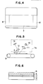
- Fig. 6 is a schematic sectional view of an optical information recording carrier of the closely contacted encapsulation type of the prior art.
- 1 is a transparent substrate made of a resin, 2 a track groove portion, 3 an optical recording layer, 4 an adhesive layer and 5 a protective substrate.
- optical writing and reading are performed for recording and reproduction of informations through the transparent substrate 1 and the track groove portion 2.
- tracking can be performed through the phase difference in the reflected light of the laser beam.
- the optical information recording carrier of the closely contacted encapsulation type obtained by forming an optical recording layer 3 on the track groove portion 2 of the transparent substrate 1 and plastering the protective substrate 5 through the adhesive layer thereon can be easily prepared.
- an optical information recording carrier of the hollow structure type having, for example, an air layer (or space layer) provided therein.
- the recording material constituting the optical recording layer is melted or sublimated by the light ⁇ heat conversion by light absorption to form recording pits, resulting in remarkable change in optical characteristics such as transmittance, reflectance, etc. at the recorded portion.
- the physical changes as mentioned above, namely the changes in shape such as pit formation, etc.
- An object of the present invention is to provide an optical information recording carrier of the closely contacted encapsulation type having cancelled the problems possessed by the optical information recording carrier of the prior art, namely improved in recording contrast and recording sensitivity.
- the optical information recording carrier according to the present invention comprises an optical recording layer provided on a transparent substrate, a film coating layer laminated with out adhesion on said optical recording layer, and further a fixing layer laminated thereon to fix said film coating layer.
- microscopic space layer may be considered to be formed, and due to the presence of such microscopic space layer, pit formation by change in shape through melting or sublimation of the optical recording layer will not be obstructed.
- a high sensitivity optical information recording carrier of the closely contacted encapsulation type improved in recording contrast can be obtained.
- Japanese Laid-open Patent Application No. 197956/1985 discloses an invention in which an organic material layer having high heat resistance and capable of absorbing surface deformation of the recording layer is formed by coating on the recording layer for the purpose of preventing deterioration of the recording layer by the adhesive layer for adhering a protective substrate or preventing inhibition of formation of pit by change in shape of the recording head by close contact with the protective substrate in an optical information recording medium of the closely contacted encapsulation type.
- This invention has no space layer existing between the recording layer and the organic material layer, because an organic material layer is formed by coating.
- the present invention has microscopic space layer existing between the recording layer and the film, because the layer provided on the recording layer is a film not adhered to the recording layer as described above, and therefore it is essentially different from the invention as described above in the point that inhibition of pit formation due to change in shape of the recording layer is prevented by the space layer.
- Fig. 1 is a schematic view of an optical information recording carrier (hereinafter written as optical recording carrier) of the close contact encapsulation type of the present invention
- Fig. 2 a sectional view showing an example of the whole constitution.
- 1 is a transparent substrate, 2 a track groove portion, 3 an optical recording layer, 6 a film coating layer, 4a a fixing layer and 5 a protective substrate.
- the optical recording carrier of the present invention comprises an optical recording layer consisting of, for example, an organic dye thin film provided on the track groove portion 2 on the transparent substrate 1 having a track groove, said optical recording layer 3 being coated on the effective recording portion 8 with a film coating layer such as a resin thin film, etc. being further laminated thereon with the fixing layer 4a comprising an adhesive, etc. to be adhered with the protective substrate 5, thereby fixing the film coating layer 6 onto the optical recording layer 3.
- the optical recording carrier of the present invention may have the optical recording layer 3 coated and fixed with the coating layer 6, and the protective substrate 5 may be either present or not.
- the film coating layer 6 in the present invention is a resin thin film, and is required to be made of a material which is not substantially changed under at least the unrecorded state of the optical recording layer at the contacted interface with the above recording layer, and should desirably prevent influence of the adhesive used in the fixing layer on the optical recording layer. Also, it should desirably be readily deformed by the heat energy which is considered to be generated by light ⁇ heat conversion in the optical recording layer of the irradiated energy.
- recording contrast and recording sensitivity can be improved without interfering with pit formation by physical deformation of the optical recording layer at all.
- thermoplastic resin thin film is preferred as the film coating layer.
- acrylic resins for example, there may be included acrylic resins, polyester type resins, polycarbonate resins, vinyl type resins, polysulfone resins, polyimide type resins, polyacetal resins, polyolefin resins, polyamide resins, vinylidene resins, cellulose derivatives or copolymers of these such as vinyl chloride-vinyl acetate copolymer, ethylene-vinyl acetate copolymer, ethylene-acrylate copolymer, vinyl acetate-acrylate copolymer, styrene-butadiene copolymer, etc.
- polyester resins particularly polyethyleneterephthalate, are preferred.
- the materials available for the protective material 5 such as sheet-shaped resins, metal thin films, etc., those which satisfy the above conditions can be all utilized.
- adhesives which satisfy the above conditions may be used. This means double use of the adhesive to be used in the fixing layer and, for example, a sheet-shaped thermoplastic adhesive can be used for the film coating layer 6.
- the above resin thin films are readily available in shape of film, with a variety of thicknesses from several ⁇ m, and its shape should be preferably smooth.
- the film should be desirably transparent to the reproducing light. In the case of detecting signals by reflectance change, there is no limitation with respect to the reproducing light employed.
- the film thickness of the film coating layer may differ depending on the material employed, but it is desired to be generally 0.05 to 100 ⁇ m, preferably 0.1 to 50 ⁇ m.
- the surface of the resin thin film constituting the film coating layer 6 may be modified only on one surface. Also, a resin thin film attached with a tacky layer functioning also as the adhesive layer may be used.
- the fixing layer 4a of the present invention is used for the purpose of fixing the above film coating layer 6 or as the adhesive layer for fixing the film coating layer 6 and plastering with the protective substrate 5.
- a thermoplastic film with lower softening temperature or melting point than the film coating layer 6 or a thermoplastic adhesive of the dry film type can be used.
- the adhesive layer in addition to those mentioned above, thermoplastic adhesives, photocurable adhesives, curable adhesives with light and heat in combination, tacky adhesives, etc, can be used without limitation, and also a protective substrate 5 with these adhesives applied on one surface may be used and plastered.
- the film coating layer 6 can be used as such for functioning also as the fixing layer 4a.
- vinyl acetate type vinyl acetate acrylic type, vinyl acetate copolymer type, vinyl acetate emulsion type, acrylic type, acrylate type, acrylic copolymer type, ethylene type, ethylene vinyl acetate type, ethylene-vinyl acetate copolymer type, polyethylene type, methylene chloride type, polyamide type, polyamide-amine type, polyimide type, urea type, epoxy type, epoxyurethane type, epoxyacrylate type, urethaneacrylate type, polyester type, chloroprene type, chloroprene rubber type, nitrile type, nitrile rubber type, urethane type, vinyl urethane type, polyurethane type, olefinic type, cyanoacrylate type, alkylacrylate type, vinyl chloride type, phenolic type, SBR type (styrene-butadiene rubber), polyol
- the transparent substrate 1 those with little inconvenience in optical recording and reproduction, and any one with high transmittance to the light used may be useful, including acrylic resins, polyester resins, polycarbonate resins, vinyl type resins, polysulfone resins, polyimide type resin, polyacetal resins, polyolefin resins, polyamide resins, cellulose derivatives, etc.
- the substrate is a thermoplastic resin
- a stamper mold is thermally transferred by such method as injection molding or hot press molding at a temperature of the melting point or higher, or the method in which a photocurable resin composition is applied on the substrate, a stamper mold is closely contacted thereon and said photocurable resin composition is cured by irradiation of UV-ray, etc., thereby phototransferring the stamper mold, etc.
- the track portion and the transparent substrate are integrally made, while in the case of the phototransfer method, the track portion and the transparent substrate are not integral but adhered together.
- a resist film may be formed on a transparent substrate having a light-transmissitve thin film with an etchable desired thickness, and exposure is effected through a photomask having a pattern of the track groove and developed to form a resist pattern, followed by etching of said thin film with the resist pattern as the mask, whereby the track portion can be also formed on the substrate.
- the width of the track groove portion may be generally 2 to 4 ⁇ m in the case of optical card, generally around 0.8 ⁇ m in the case of optical disc, with the track pitch being 8 ⁇ m to 15 ⁇ m in the former, and around 1.6 ⁇ m in the latter.
- the depth of the groove may be preferably ⁇ /4n (or ⁇ /8n) multiplied by an odd number wherein ⁇ is the wavelength of the light source employed and n is the refractive index of the transparent substrate 1, for detection of tracking signals.
- ⁇ is the wavelength of the light source employed
- n is the refractive index of the transparent substrate 1, for detection of tracking signals.
- the optical recording layer 3 is formed on the track groove portion 2, for the purpose of improving adhesiveness, improving optical characteristics (e.g. transmittance or reflectance), improving gas barrier property to gas release from the substrate, improving thermal conductivity for storage stability of the optical recording layer or prevention of deterioration by the reproducing light, etc., UV-ozone treatment, plasma treatment, etc. may be applied.
- the recording layer 3 should be preferably greater in difference between the reflectance at the pit, etc. which is the recorded portion and the reflectance at the unrecorded portion at around the wavelength of the reproducing light employed, for example, the semiconductor laser wavelength region, and also preferably one which is not changed in reflectances at the recorded portion and the unrecorded portion by the reproducing light. Further, it should preferably be one with smaller energy required for pit formation during recording.
- oxides such as of Te, Sb, Mo, Ge, V, Sn, etc.
- compounds such as Te-Sn, TeOx-Ge, etc.
- complex compounds of metals with organic compounds or inorganic sulfides such as Te-CH4, Te-CS2, Te-styrene, Sn-SO2, GeS-Sn, SnS-S, etc.
- thermoplastic resins such as nitrocellulose, polystyrene, polyethylene, etc. containing metal particles such as silver, etc. dispersed therein, such thermoplastic resins having metal particles agglomerated on the surface thereof, chalcogenides or chromogenic type MoO3-Cu, MoO3-Sn-Cu, etc.
- improvement in effect of the recording contrast is marked when an organic dye capable of undergoing optical physical change is used.
- the recording layer in the optical information recording carrier of the close contact encapsulation type of the prior art comprises an organic dye film capable of undergoing physical change, it is susceptible to the action of inhibiting pit formation by the upper layer of the recording layer, for example, a protective substrate.
- organic dye to be used in the organic thin film there may included, for example, anthraquinone derivatives (particularly those having indanthrene skelton), dioxazine compound and derivatives thereof, triphenodithiazine compounds, phenanthrene derivatives, cyanine compounds, melocyanine compounds, pyrilium type compounds, xanthene type compounds, triphenylmethane type compounds, croconium type dyes, azo dyes, crocones, azines, indigoids, polymethine type dyes, azulenes, squarilium derivatives, sulfide dyes and dithiolate complexes of metals, etc.
- anthraquinone derivatives particularly those having indanthrene skelton
- dioxazine compound and derivatives thereof triphenodithiazine compounds
- phenanthrene derivatives cyanine compounds
- melocyanine compounds pyrilium type compounds
- the quenching agent may be selected from those as mentioned below in view of compatibility with the dye and the solvent.
- the amount added can vary from several % by weight to 50% by weight. If it is too small, no considerable effect as the quenching agent can be seen, while if added in an amount over 50% by weight, reduction in sensitivity is observed due to lowering in the absolute amount of the heat mode recording material. Accordingly, an amount of 10% by weight to 30% by weight based on the dye is preferred. Particularly, high effect without accompaniment of deterioration in sensitivity can be obtained from around 20% by weight.
- various metal chelate compounds particularly comprising multi-dentate ligands with Zn, Cu, Ni, Cr, Co, Mn, Pd, Zr as the center atom, for example, tetradentate ligands such as N4, N2O2, N2S2, S4, O2S2, O4, etc., or tridentate ligands such as N2O, NO2, NS2, O3, NOS, etc.
- ligand such as water, ammonia, halogen, phosphine, amine, arsine, olefin, etc., or the tetradentate type with two bidentate ligands N2, NO, O2, S2, otherwise biscyclopentadienyl ligand, cyclopentadienyl-tropyrinium ligand system, or those comprising combinations of the above ligands, and otherwise various aromatic amines or diamines, nitrogen-containing aromatic compounds and onium salts thereof, such as aminium salts, diimonium salts, pyridinium salts, imidazolinium salts, quinolinium salts, etc.
- pyrylium salts which are salts of oxygen-containing aromatic compounds, etc. may be also used. Also, it is possible to use a plural number of these quenching agents in combination, and the composition ratios can be suitably varied in view of coatability of the dye composition, stability of the coated film, optical characteristics (reflectance and transmittance), recording sensitivity, etc.
- the optical recording layer 3 comprising the above organic dye or dye composition may be formed according to the known coating method. For example, there may be employed such method as dip coating, spray coating, spinner coating, bar coating, blade coating, roll coating, curtain coating, etc.
- the thickness of the optical recording layer 3 may be generally about 500 to 2000 ⁇ , preferably around 1000 ⁇ . Particularly, with respect to recording sensitivity, the thickness should be preferably thinner, while it is peferably thicker with respect to the S/N ratio during reproduction, and its optimum film thickness may differ depending on the kind of the dye.
- the protective substrate 5 all materials available as conventional protective substrate can be used, including specifically polyvinyl chloride, fluorine-substituted ethylene polymer, vinyl chloride-vinyl acetate copolymer, polyvinylidene chloride, acrylic polymers such as polymethyl methacrylate, polystyrene, polyvinyl butyral, acetyl cellulose, styrene-butadiene copolymer, polyethylene, polypropylene, polycarbonate, epoxyacrylonitrile-butadiene-styrene copolymer, etc.
- polyvinyl chloride fluorine-substituted ethylene polymer
- vinyl chloride-vinyl acetate copolymer polyvinylidene chloride
- acrylic polymers such as polymethyl methacrylate, polystyrene, polyvinyl butyral, acetyl cellulose, styrene-butadiene copolymer
- polyethylene polyprop
- a diversity of materials can be used depending on the uses, including metal sheets of iron, stainless steel, aluminum, tin, copper, zinc, etc., synthetic paper, paper, fiber-reinforced plastic, composite materials of metal powder such as magnetic material with plastic, ceramics, etc.
- metal sheets of iron, stainless steel, aluminum, tin, copper, zinc, etc. synthetic paper, paper, fiber-reinforced plastic, composite materials of metal powder such as magnetic material with plastic, ceramics, etc.
- those used for the transparent substrate 1 may be used.
- the film coating layer covers the optical recording layer effective portion 7 of the optical recording layer 3, namely the recording region.
- the portion of the recording layer other than the recording region is penetrated with the adhesive used for the fixing layer, and further formed into a completely adhered structure, whereby the recording sensitivity is lowered but the recording region portion has ordinary recording density, as optimum for the constitution of an optical recording carrier shaped in a card (hereinafter called optical card). More specifically, as shown in Fig.
- the optical card moves toward arrowhead A by the rotating mechanism 9 when tracking is performed during reproduction to read the information, but the optical card will stop temporarily after completion toward the A direction before movement toward the opposite direction, whereby writing proceeds with the energy of the reproducing light at that portion, namely the marginal portion, although extremely gradually, until reaching the state where the tracking signal can be detected with difficulty, as is well known in the art. Accordingly, it is desirable that the marginal portion 8 should be lower in recording sensitivity and the tracking signal can be read.
- the track groove portion is not integrated with the substrate, but it is a laminated structure.
- the track portion comprises a photocured resin, even with an extremely thin layer of several ⁇ m to some 100 ⁇ m, it has been observed that the characteristics of a cured resin tend to be exhibited strongly. For this reason, in the case of an optical information recording carier, pit formation due to physical change such as melting, sublimation, etc.
- the recording sensitivity of the optical recording layer can be inhibited greatly, whereby the recording sensitivity becomes very low.
- the recording sensitivity can be restored at the recording region portion 7, whereby recording can be effected with good sensitivity in the recording region, while recording sensitivity is very low at the marginal portion to give rise to substantially no deterioration with the reproducing light.
- the film coating layer 6 has been found to be good in thermostat humidistat durability as compared with the optical recording carrier of a hollow structure. This may be considered to be due to the fact that the film coating layer 6 also functions as the protective layer for the optical recording layer, whereby no deterioration of the recording layer occurs due to oxygen, moisture, etc. remaining at the hollow portion of the optical recording carrier of a hollow structure.
- an optical information recording medium of the closely contacted encapsulation type with a simple constitution improved in recording sensitivity and recording contrast can be obtained.
- a track groove was formed according to the 2P molding method by use of a photocurable resin mixture comprising neopentyl glycol diacrylate (70 parts by weiht), a bisphenol type epoxy acrylate (30 parts by weight) (bifunctional acrylate having acrylic acid added on Epikote (trade name) produced by Yuka Shell Epoxy) and benzoin isopropyl ether (1 part by weight).
- a photocurable resin mixture comprising neopentyl glycol diacrylate (70 parts by weiht), a bisphenol type epoxy acrylate (30 parts by weight) (bifunctional acrylate having acrylic acid added on Epikote (trade name) produced by Yuka Shell Epoxy) and benzoin isopropyl ether (1 part by weight).
- a substrate for optical card comprising a stripe-shaped track groove with a track groove of 3 ⁇ m, a track groove pitch of 13 ⁇ m and a track depth of 1300 ⁇ .
- Said substrate for optical card was dried at 120 °C for 3 hours to remove residual monomers and complete the polymerization, and Colcoat 103X (produced by Colcoat) was applied as the subbing layer by the spin coating method, followed by drying at 50°C for 3 hours to form a silica thin film of 500 ⁇ .
- a solution of a dye of the formula (I) shown below dissolved to 6% by weight in dichloroethane was applied by the spin coating method to form an optical recording layer with a thickness of 1000 ⁇ .
- a polyethylene-terephthalate shaped in a strip with a thickness of 5 ⁇ m Lumirror, produced by Toray K.K. was superposed and further a thermoplastic adhesive (ethylene-vinyl acetate type dry film) with a thickness of 50 ⁇ m superposed thereon, and a white polycarbonate of 0.3 mm (Toughlon, produced by Idemitsu Sekiyu Kagaku K.K.) was superposed as the opaque card substrate, followed by hot pressurization with hot rolls with a surface tempeerature of 110 °C to prepare an optical card.
- the contrast ratio represents a ratio of the reflectance at the non-recorded portion relative to the value of the reflectance at the non-recorded portion from which the reflectance at the recorded portion is detracted.
- a subbing layer comprising a silica thin film with a thickness of 200 ⁇ was formed by spin coating of Colcoat 103X (produced by Colcoat) on an acrylic disc substrate (diameter 130 mm, inner diameter 15 mm) grooved with a track groove of 0.8 ⁇ m, a track pitch of 1.6 ⁇ m and a track groove depth of 600 ⁇ .
- an optical recording layer with a thickness of 900 ⁇ by coating of a 2% by weight of a dichloroethane solution of a dye of the formula (II) shown below added with 20% by weight based on the dye of N,N,N ⁇ ,N ⁇ -tetrakis(p-di-n-butylaminophenyl)-p-phenylenediimmonium perchlorate (the formula (III)) as the quenching agent.
- a polyester film shaped in a ring band with a diameter of 125 mm, an inner diameter of 30 mm and a thickness of 5 ⁇ m (trade name: Tetron F, produced by Teijin Kasei), and further a tackifier-attached triacetate film (70 ⁇ m thickness) with a diameter of 130 mm and an inner diameter of 15 mm was pressure adhered and laminated at normal temperature to obtain an optical disc of the close contact encapsulation type.
- An optical disc was prepared in entirely the same manner as in Example 2 except for omitting the 5 ⁇ m polyester film which was the film coating layer. As the result, the tackifier appeared to have reacted with the optical recording layer, whereby reflectance was lowered to make recording impossible.
- a disc substrate was prepared in entirely the same manner as in Example 2 to the step of forming the optical recording layer.
- a UV-curable adhesive having styrene-divinylbenzene resin beads with particle size of 300 ⁇ m dispersed therein in ring bands of 2 mm in width and, with the disc substrate attached with the optical recording layer superposed thereon, UV-ray was irradiated with the portion corresponding to the optical recording layer intercepted from light to cure the ring bands, to prepare an optical disc having a space layer.
- An optical disk was manufactured by the same manner as in Example 2 except that a thermoplastic dry film (ethylene-vinyl acetate type, thickness of 50 ⁇ m) with a release paper used in place of a triacetate film (thickness of 70 ⁇ m) on which an adhesive is coated was laminated by a thermocompression bonding at 110 °C, and the release paper was peeled.
- a contrast ratio was 0.72.
- the track groove portion was coated by bar coating with a dye having the structure of the following formula (IV) to form an optical recording layer with a film thickness of 0.1 ⁇ m.
- the effective portion of the optical layer formed on the track groove portion, namely the recording region was covered with a 5 ⁇ m polyethyleneterephthalate film, and a polycarbonate with a thickness of 300 ⁇ m was adhered onto the protective substrate by use a polyamide type adhesive to prepare a card, whereby reflectance of light of 15% and sufficient adhesion strength could be obtained.
- the contrast was found to be 0.78 .
- a card-shaped optical recording medium was prepared in entirely the same manner as in Example 4 except for omitting the 5 ⁇ m polyethyleneterephthalate film which was the film coating layer and using a ethylene-vinyl acetate adhesive.
- the reflectance of the light at 830 nm was 15%, but the adhesive strength between the grooved polycarbonate and the polycarbonate as the card substrate was low.
- the contrast ratio was found to be 0.61.
- An optical card was prepared in entirely the same manner as in Example 4 except for omitting the 5 ⁇ m polyethyleneterephthalate film which was the film coating layer and using a polyamide type adhesive.
- the adhesive strength was high.
- the reflectance of the light at 830 nm was lowered to make recording impossible.
- a track groove was formed according to the 2P molding method by use of a photocurable resin mixture comprising neopentyl glycol diacrylate (70 parts by weiht), a bisphenol type epoxy acrylate (30 parts by weight) (bifunctional acrylate having acrylic acid added on Epikote (trade name) produced by Yuka Shell Epoxy) and benzoin isopropyl ether (1 part by weight).
- a substrate for optical card comprising a stripe-shaped track groove with a track groove of 3 ⁇ m, a track groove pitch of 13 ⁇ m and a track depth of 1300 ⁇ .
- Said substrate for optical card was dried at 120 °C for 3 hours to remove residual monomers and complete the polymerization, and Colcoat 103X (produced by Colcoat) was applied as the subbing layer by the spin coating method, followed by drying at 50 °C for 3 hours to form a silica thin film of 500 ⁇ .
- a solution of a dye of the formula (V) shown below dissolved to 1.6% by weight in dichloroethane was applied by the spin coating method to form an optical recording layer with a thickness of 1000 ⁇ .
- the contrast ratio at the marginal portion was found to be 0.2 or less, thus giving substantially low value as the recording contrast ratio.
- the contrast ratio represents a ratio of the reflectance at the non-recorded portion relative to the value of the reflectance at the non-recorded portion from which the reflectance at the recorded portion is detracted.
Landscapes
- Thermal Transfer Or Thermal Recording In General (AREA)
Applications Claiming Priority (4)
| Application Number | Priority Date | Filing Date | Title |
|---|---|---|---|
| JP40419/87 | 1987-02-25 | ||
| JP40415/87 | 1987-02-25 | ||
| JP62040419A JPH0827995B2 (ja) | 1987-02-25 | 1987-02-25 | 光学的情報記録担体 |
| JP62040415A JPH0827994B2 (ja) | 1987-02-25 | 1987-02-25 | 光カ−ド |
Publications (3)
| Publication Number | Publication Date |
|---|---|
| EP0280531A2 true EP0280531A2 (de) | 1988-08-31 |
| EP0280531A3 EP0280531A3 (en) | 1989-05-17 |
| EP0280531B1 EP0280531B1 (de) | 1993-09-15 |
Family
ID=26379884
Family Applications (1)
| Application Number | Title | Priority Date | Filing Date |
|---|---|---|---|
| EP19880301586 Expired - Lifetime EP0280531B1 (de) | 1987-02-25 | 1988-02-24 | Optischer Datenaufzeichnungsträger |
Country Status (3)
| Country | Link |
|---|---|
| US (1) | US4871601A (de) |
| EP (1) | EP0280531B1 (de) |
| DE (1) | DE3884013T2 (de) |
Cited By (3)
| Publication number | Priority date | Publication date | Assignee | Title |
|---|---|---|---|---|
| EP0407931A3 (en) * | 1989-07-12 | 1992-07-29 | Laser Technology Sdn. Bhd. | Laser recording medium |
| US5432770A (en) * | 1991-02-08 | 1995-07-11 | Canon Kabushiki Kaisha | Optical recording medium, method of reproducing recorded data of optical recording medium, and system for reproducing recorded data of optical recording medium |
| EP0896328A1 (de) * | 1997-07-29 | 1999-02-10 | Victor Company Of Japan, Ltd. | Informationsaufzeichnungsträger und Verfahren zu dessen Herstellung |
Families Citing this family (23)
| Publication number | Priority date | Publication date | Assignee | Title |
|---|---|---|---|---|
| JPS6412224U (de) * | 1987-07-08 | 1989-01-23 | ||
| US5249176A (en) * | 1987-07-20 | 1993-09-28 | Canon Kabushiki Kaisha | Optical recording medium, process for preparing the same and its optical recording and reproducing system |
| US5328816A (en) * | 1988-09-13 | 1994-07-12 | Canon Kabushiki Kaisha | Process for producing optical recording medium |
| DE68925517T2 (de) * | 1988-11-16 | 1996-06-05 | Canon Kk | Verfahren zur Herstellung von Bildplatten |
| JP2551474B2 (ja) * | 1988-11-28 | 1996-11-06 | キヤノン株式会社 | 光記録媒体およびその製造方法 |
| US5002622A (en) * | 1989-02-27 | 1991-03-26 | Del Mar Avionics | Glass based optical disc manufacturing process |
| JPH02226533A (ja) * | 1989-02-27 | 1990-09-10 | Mitsubishi Electric Corp | 情報記録媒体 |
| JP2880180B2 (ja) * | 1989-03-28 | 1999-04-05 | キヤノン株式会社 | 記憶媒体 |
| EP0404521A3 (de) * | 1989-06-21 | 1991-05-02 | Hitachi Maxell Ltd. | Optischer Aufzeichnungsträger und dessen Herstellungsverfahren |
| JP3015053B2 (ja) * | 1989-10-12 | 2000-02-28 | キヤノン株式会社 | 光学記録媒体 |
| US5270150A (en) * | 1990-04-25 | 1993-12-14 | Victor Company Of Japan, Ltd. | Optical recording medium and process for producing it |
| DE69127398T2 (de) * | 1990-05-22 | 1998-01-02 | Canon Kk | Verfahren und Gerät zur Aufzeichnung und Wiedergabe von Informationen in Zellen, die eine vielfache Interferenz gebrauchen |
| DE69231842T2 (de) * | 1991-08-02 | 2001-10-31 | Canon K.K., Tokio/Tokyo | Optisches Aufzeichnungsmedium, Verfahren zu dessen Herstellung, und Datenaufzeichnungsverfahren |
| US5482822A (en) * | 1992-05-12 | 1996-01-09 | Canon Kabushiki Kaisha | Infrared-absorptive compound and optical recording medium making use of the same |
| US5428599A (en) * | 1992-06-18 | 1995-06-27 | Canon Kabushiki Kaisha | Optical recording medium, information recording method and information reproducing method |
| US5503888A (en) * | 1992-06-19 | 1996-04-02 | Canon Kabushiki Kaisha | Optical recording medium, substrate for optical recording medium, and method for preparing substrate for optical recording medium |
| US5368988A (en) * | 1992-09-11 | 1994-11-29 | Tdk Corporation | Optical recording medium |
| US5527497A (en) * | 1992-11-26 | 1996-06-18 | Canon Kabushiki Kaisha | Process and apparatus for manufacturing substrate sheet for optical recording mediums, and process for preparing stamper |
| CA2110233C (en) | 1992-12-02 | 1999-01-12 | Mitsui Toatsu Chemicals, Incorporated | Optical information recording medium and composition for optical information recording film |
| US5505769A (en) * | 1993-08-02 | 1996-04-09 | Munters Corporation | Titanium silicate aerogel element and humidity exchanger using matrix of aerogel element |
| US6527904B1 (en) * | 1996-11-14 | 2003-03-04 | Pioneer Electronic Corporation | Method of producing an optical video disc |
| TW564408B (en) * | 2001-11-09 | 2003-12-01 | Ritek Corp | Method and structure to increase the track-following signal of optical disk |
| WO2006035496A1 (ja) * | 2004-09-28 | 2006-04-06 | Fujitsu Limited | α線量率測定方法 |
Family Cites Families (7)
| Publication number | Priority date | Publication date | Assignee | Title |
|---|---|---|---|---|
| US4435801A (en) * | 1979-12-28 | 1984-03-06 | Rca Corporation | Information record with a thick overcoat |
| US4340655A (en) * | 1980-06-18 | 1982-07-20 | Eastman Kodak Company | Thermal and mechanical barrier layers for optical recording elements |
| JPS57130243A (en) * | 1981-02-05 | 1982-08-12 | Toshiba Corp | Information storage medium |
| JPS5845635A (ja) * | 1981-09-08 | 1983-03-16 | Fujitsu Ltd | 記録媒体 |
| JPS5977647A (ja) * | 1982-10-26 | 1984-05-04 | Matsushita Electric Ind Co Ltd | 光学式円盤 |
| JPS5990248A (ja) * | 1982-11-15 | 1984-05-24 | Sony Corp | 情報記録媒体 |
| JPS60197956A (ja) * | 1984-03-21 | 1985-10-07 | Nec Home Electronics Ltd | 光デイスク |
-
1988
- 1988-02-22 US US07/159,310 patent/US4871601A/en not_active Expired - Lifetime
- 1988-02-24 DE DE88301586T patent/DE3884013T2/de not_active Expired - Fee Related
- 1988-02-24 EP EP19880301586 patent/EP0280531B1/de not_active Expired - Lifetime
Cited By (4)
| Publication number | Priority date | Publication date | Assignee | Title |
|---|---|---|---|---|
| EP0407931A3 (en) * | 1989-07-12 | 1992-07-29 | Laser Technology Sdn. Bhd. | Laser recording medium |
| US5432770A (en) * | 1991-02-08 | 1995-07-11 | Canon Kabushiki Kaisha | Optical recording medium, method of reproducing recorded data of optical recording medium, and system for reproducing recorded data of optical recording medium |
| EP0896328A1 (de) * | 1997-07-29 | 1999-02-10 | Victor Company Of Japan, Ltd. | Informationsaufzeichnungsträger und Verfahren zu dessen Herstellung |
| US6083597A (en) * | 1997-07-29 | 2000-07-04 | Victor Company Of Japan, Ltd. | Information recording carrier and manufacturing method thereof |
Also Published As
| Publication number | Publication date |
|---|---|
| DE3884013D1 (de) | 1993-10-21 |
| EP0280531A3 (en) | 1989-05-17 |
| EP0280531B1 (de) | 1993-09-15 |
| DE3884013T2 (de) | 1994-03-03 |
| US4871601A (en) | 1989-10-03 |
Similar Documents
| Publication | Publication Date | Title |
|---|---|---|
| US4871601A (en) | Optical information recording carrier | |
| US5415914A (en) | Optical recording disk | |
| US4954380A (en) | Optical recording medium and process for production thereof | |
| US5248584A (en) | Optical card and method for reading information recorded in it | |
| US5248990A (en) | Process for producing optical recording medium for optical data recording and reproduction | |
| US5328816A (en) | Process for producing optical recording medium | |
| EP0566233B1 (de) | Optisches Speichermedium und Informationsaufzeichnungsverfahren mit diesem | |
| EP0259151B1 (de) | Optische Karte und Verfahren zu ihrer Herstellung | |
| US5432770A (en) | Optical recording medium, method of reproducing recorded data of optical recording medium, and system for reproducing recorded data of optical recording medium | |
| US5264327A (en) | Method for preparing information recording medium | |
| JPH0827995B2 (ja) | 光学的情報記録担体 | |
| US5645907A (en) | Organic optical recording medium and method for the prevention of rewrite therein | |
| JPH04307444A (ja) | 光記録担体及びその製造方法 | |
| JPH0827994B2 (ja) | 光カ−ド | |
| JP2517645B2 (ja) | 光記録媒体 | |
| JP2763395B2 (ja) | 光記録媒体 | |
| JPH01287842A (ja) | 光記録媒体 | |
| JP2515553B2 (ja) | 光カ―ド | |
| JP2515554B2 (ja) | 光カ―ド | |
| JP2510803B2 (ja) | 光記録媒体 | |
| JP3092846B2 (ja) | 光カード | |
| JPH0814898B2 (ja) | 光カード | |
| JPH031339A (ja) | 光カード | |
| EP0287394A2 (de) | Verfahren zur Herstellung von einem optischen Datenträger | |
| JP2793516B2 (ja) | 光情報記録媒体とその再生方法 |
Legal Events
| Date | Code | Title | Description |
|---|---|---|---|
| PUAI | Public reference made under article 153(3) epc to a published international application that has entered the european phase |
Free format text: ORIGINAL CODE: 0009012 |
|
| AK | Designated contracting states |
Kind code of ref document: A2 Designated state(s): DE FR GB |
|
| PUAL | Search report despatched |
Free format text: ORIGINAL CODE: 0009013 |
|
| AK | Designated contracting states |
Kind code of ref document: A3 Designated state(s): DE FR GB |
|
| 17P | Request for examination filed |
Effective date: 19891014 |
|
| 17Q | First examination report despatched |
Effective date: 19910412 |
|
| GRAA | (expected) grant |
Free format text: ORIGINAL CODE: 0009210 |
|
| AK | Designated contracting states |
Kind code of ref document: B1 Designated state(s): DE FR GB |
|
| REF | Corresponds to: |
Ref document number: 3884013 Country of ref document: DE Date of ref document: 19931021 |
|
| ET | Fr: translation filed | ||
| PLBE | No opposition filed within time limit |
Free format text: ORIGINAL CODE: 0009261 |
|
| STAA | Information on the status of an ep patent application or granted ep patent |
Free format text: STATUS: NO OPPOSITION FILED WITHIN TIME LIMIT |
|
| 26N | No opposition filed | ||
| REG | Reference to a national code |
Ref country code: GB Ref legal event code: IF02 |
|
| PGFP | Annual fee paid to national office [announced via postgrant information from national office to epo] |
Ref country code: GB Payment date: 20030210 Year of fee payment: 16 |
|
| PGFP | Annual fee paid to national office [announced via postgrant information from national office to epo] |
Ref country code: FR Payment date: 20030220 Year of fee payment: 16 |
|
| PGFP | Annual fee paid to national office [announced via postgrant information from national office to epo] |
Ref country code: DE Payment date: 20030221 Year of fee payment: 16 |
|
| PG25 | Lapsed in a contracting state [announced via postgrant information from national office to epo] |
Ref country code: GB Free format text: LAPSE BECAUSE OF NON-PAYMENT OF DUE FEES Effective date: 20040224 |
|
| PG25 | Lapsed in a contracting state [announced via postgrant information from national office to epo] |
Ref country code: DE Free format text: LAPSE BECAUSE OF NON-PAYMENT OF DUE FEES Effective date: 20040901 |
|
| GBPC | Gb: european patent ceased through non-payment of renewal fee |
Effective date: 20040224 |
|
| PG25 | Lapsed in a contracting state [announced via postgrant information from national office to epo] |
Ref country code: FR Free format text: LAPSE BECAUSE OF NON-PAYMENT OF DUE FEES Effective date: 20041029 |
|
| REG | Reference to a national code |
Ref country code: FR Ref legal event code: ST |