EP0287394A2 - Verfahren zur Herstellung von einem optischen Datenträger - Google Patents
Verfahren zur Herstellung von einem optischen Datenträger Download PDFInfo
- Publication number
- EP0287394A2 EP0287394A2 EP88303428A EP88303428A EP0287394A2 EP 0287394 A2 EP0287394 A2 EP 0287394A2 EP 88303428 A EP88303428 A EP 88303428A EP 88303428 A EP88303428 A EP 88303428A EP 0287394 A2 EP0287394 A2 EP 0287394A2
- Authority
- EP
- European Patent Office
- Prior art keywords
- optical recording
- organic film
- process according
- recording layer
- laser light
- Prior art date
- Legal status (The legal status is an assumption and is not a legal conclusion. Google has not performed a legal analysis and makes no representation as to the accuracy of the status listed.)
- Granted
Links
Images



Classifications
-
- G—PHYSICS
- G11—INFORMATION STORAGE
- G11B—INFORMATION STORAGE BASED ON RELATIVE MOVEMENT BETWEEN RECORD CARRIER AND TRANSDUCER
- G11B7/00—Recording or reproducing by optical means, e.g. recording using a thermal beam of optical radiation by modifying optical properties or the physical structure, reproducing using an optical beam at lower power by sensing optical properties; Record carriers therefor
- G11B7/24—Record carriers characterised by shape, structure or physical properties, or by the selection of the material
- G11B7/241—Record carriers characterised by shape, structure or physical properties, or by the selection of the material characterised by the selection of the material
- G11B7/242—Record carriers characterised by shape, structure or physical properties, or by the selection of the material characterised by the selection of the material of recording layers
- G11B7/244—Record carriers characterised by shape, structure or physical properties, or by the selection of the material characterised by the selection of the material of recording layers comprising organic materials only
-
- G—PHYSICS
- G11—INFORMATION STORAGE
- G11B—INFORMATION STORAGE BASED ON RELATIVE MOVEMENT BETWEEN RECORD CARRIER AND TRANSDUCER
- G11B7/00—Recording or reproducing by optical means, e.g. recording using a thermal beam of optical radiation by modifying optical properties or the physical structure, reproducing using an optical beam at lower power by sensing optical properties; Record carriers therefor
- G11B7/002—Recording, reproducing or erasing systems characterised by the shape or form of the carrier
- G11B7/0033—Recording, reproducing or erasing systems characterised by the shape or form of the carrier with cards or other card-like flat carriers, e.g. flat sheets of optical film
-
- G—PHYSICS
- G11—INFORMATION STORAGE
- G11B—INFORMATION STORAGE BASED ON RELATIVE MOVEMENT BETWEEN RECORD CARRIER AND TRANSDUCER
- G11B7/00—Recording or reproducing by optical means, e.g. recording using a thermal beam of optical radiation by modifying optical properties or the physical structure, reproducing using an optical beam at lower power by sensing optical properties; Record carriers therefor
- G11B7/08—Disposition or mounting of heads or light sources relatively to record carriers
- G11B7/09—Disposition or mounting of heads or light sources relatively to record carriers with provision for moving the light beam or focus plane for the purpose of maintaining alignment of the light beam relative to the record carrier during transducing operation, e.g. to compensate for surface irregularities of the latter or for track following
- G11B7/0938—Disposition or mounting of heads or light sources relatively to record carriers with provision for moving the light beam or focus plane for the purpose of maintaining alignment of the light beam relative to the record carrier during transducing operation, e.g. to compensate for surface irregularities of the latter or for track following servo format, e.g. guide tracks, pilot signals
-
- G—PHYSICS
- G11—INFORMATION STORAGE
- G11B—INFORMATION STORAGE BASED ON RELATIVE MOVEMENT BETWEEN RECORD CARRIER AND TRANSDUCER
- G11B7/00—Recording or reproducing by optical means, e.g. recording using a thermal beam of optical radiation by modifying optical properties or the physical structure, reproducing using an optical beam at lower power by sensing optical properties; Record carriers therefor
- G11B7/24—Record carriers characterised by shape, structure or physical properties, or by the selection of the material
- G11B7/26—Apparatus or processes specially adapted for the manufacture of record carriers
-
- G—PHYSICS
- G11—INFORMATION STORAGE
- G11B—INFORMATION STORAGE BASED ON RELATIVE MOVEMENT BETWEEN RECORD CARRIER AND TRANSDUCER
- G11B21/00—Head arrangements not specific to the method of recording or reproducing
- G11B21/02—Driving or moving of heads
- G11B21/08—Track changing or selecting during transducing operation
- G11B21/081—Access to indexed tracks or parts of continuous track
- G11B21/083—Access to indexed tracks or parts of continuous track on discs
-
- G—PHYSICS
- G11—INFORMATION STORAGE
- G11B—INFORMATION STORAGE BASED ON RELATIVE MOVEMENT BETWEEN RECORD CARRIER AND TRANSDUCER
- G11B23/00—Record carriers not specific to the method of recording or reproducing; Accessories, e.g. containers, specially adapted for co-operation with the recording or reproducing apparatus ; Intermediate mediums; Apparatus or processes specially adapted for their manufacture
- G11B23/0014—Record carriers not specific to the method of recording or reproducing; Accessories, e.g. containers, specially adapted for co-operation with the recording or reproducing apparatus ; Intermediate mediums; Apparatus or processes specially adapted for their manufacture record carriers not specifically of filamentary or web form
- G11B23/0021—Record carriers not specific to the method of recording or reproducing; Accessories, e.g. containers, specially adapted for co-operation with the recording or reproducing apparatus ; Intermediate mediums; Apparatus or processes specially adapted for their manufacture record carriers not specifically of filamentary or web form discs
- G11B23/0028—Details
- G11B23/0035—Details means incorporated in the disc, e.g. hub, to enable its guiding, loading or driving
- G11B23/0042—Details means incorporated in the disc, e.g. hub, to enable its guiding, loading or driving with provision for auxiliary features
Definitions
- the present invention relates to a process for producing an optical recording medium for optical data recording and reproduction.
- optical recording media for recording and reproduction of optical data, such as optical disks, optical cards and optical tapes as effective means for processing a wide variety of data.
- optical recording media there is known a type wherein binary-coded data are recorded and detected as a change in reflectivity or change in surface shape, such as presence or absence of pits, yielding a change in reflected light intensity.
- DRAW direct read after write
- a system of forming grooves at a certain interval on the surface of a substrate as tracking servo guides for writing and reading is known.
- the grooves function as guides for writing and reading, the tracking control accuracy of a laser beam is improved and a higher access speed can be accomplished than the conventional system using a substrate with no such guide grooves.
- a method of thermally transferring a stamper pattern by injection molding or hot pressing at a temperature above the melting point of a thermoplastic resin is known in case where the substrate is composed of such a thermoplastic resin, and also known is a method wherein a photosetting resin composition is applied onto a substrate and is cured under irradiation with ultraviolet rays, etc. and in contact with a stamper to photo-transfer the stamper pattern.
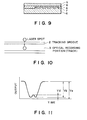
- Figure 9 is a schematic sectional view of a conventional optical recording medium in the form of a card, which comprises a substrate 6 having tracking patterns 6, an adhesive layer 4, and a base 5.
- the optical recording medium is used for recording and reproduction of data by writing and readout by means of the substrate 6 and the track 7.
- the track 7 is integral with and made of the same material as the substrate 6.
- the track 7 is not made of the same material as but is bonded to the substrate 6.
- the substrate 6 is preliminarily provided with tracking grooves so as to allow tracking by phase lag of a laser beam through utilization of the fine unevenness pattern.
- Such an optical recording medium has a structure comprising an optical recording layer formed on an uneven surface, so that the production thereof requires formation of an unevenness pattern on the substrate first of all.
- the conventional transfer process using a stamper involves several problems with respect to the yield of transfer of a stamper pattern, transfer time, and the durability and cost of the stamper affecting the productivity and production cost of the optical recording medium.
- the recording sensitivity of the optical recording layer depends on the thickness of the layer, it is necessary to form the optical recording layer in a uniform thickness.
- the optical recording layer was conventionally formed on an uneven substrate surface, it was difficult to form the layer in a uniform thickness. Further, the groove pattern was not well reproduced on the optical recording layer, so that a good tracking signal could not be obtained.
- An object of the present invention is to provide a process for producing an optical recording medium having an optical recording layer of an organic film which is capable of forming a tracking groove without using a stamper.
- Another object of the present invention is to provide a process for producing an optical recording medium capable of producing a high-quality tracking signal.
- a further object of the present invention is to provide a process for producing an optical recording medium, which comprises considerably higher steps than the conventional processes.
- a process for producing an optical recording medium which comprises forming an optical recording layer comprising an organic film on a substrate, and irradiating the organic film with laser light to scatter the irradiated portion of the organic film, thus forming a tracking groove thereat and leaving an optical recording part along the tracking groove.
- a tracking groove may be formed without a developing treatment after the irradiation with the laser beam, so that an optical recording medium of an organic film may be provided with a tracking groove without using a stamper and a good tracking signal may be obtained.
- a good tracking signal may be obtained presumably because of a large difference in reflectivity between the optical recording part (track) and tracking groove, a phase difference in reflected light, and a combined effect of these.
- each optical recording medium comprises a substrate 1, tracking grooves 2, optical recording parts (tracks) 3, an adhesive layer 4, and a base 5.
- a tracking groove 2 may preferably have a width of 2 - 4 ⁇ m, and an optical recording part 3 may preferably have a width of 3 - 10 ⁇ . It is preferred that the tracking groove 2 is substantially face of the organic film constituting the optical recording part (as shown in Figure 1) or only with a slightly remaining film after scattering (as shown in Figure 2) such that it provides a difference in reflectivity satisfying the relationship of 0.3 ⁇ (R(d1)--R(d2))/R(d1) ⁇ 0.7, wherein R(d1) denotes the reflectivity at the optical recording part and R(d2) denotes the reflectivity at the tracking groove, in order to obtain a good tracking signal.
- the tracking groove 2 and the optical recording part 3 provide a reflective contrast of 0.45 or above.
- the reflective contrast is measured by using an ordinary optical readout system (e.g., one including a semiconductor laser of 830 nm at a power of 0.27 mW) and scanning an optical recording medium across a tracking groove with a laser beam spot (of, e.g., 3 ⁇ m diameter) as shown in Figure 10A and calculating the contrast according to the following definition based on a reflected light quantity curve as shown in Figure 10 detected by an oscilloscope connected to the readout system:
- an ordinary optical readout system e.g., one including a semiconductor laser of 830 nm at a power of 0.27 mW
- a laser beam spot of, e.g., 3 ⁇ m diameter
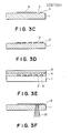
- FIGS 3A - 3E illustrate an embodiment of the invention wherein an optical recording layer 9 formed on a substrate 1 is irradiated with a scanning laser beam 10 condensed or focused to a tracking groove width. More specifically, an organic film 9 constituting an optical recording layer is formed on a substrate 1 ( Figure 3A). Then, the organic film 9 is irradiated with scanning laser light 10 having a wavelength absorbable by the organic film and condensed to a desired tracking groove width ( Figure 3B), thereby to form a tracking groove 2 ( Figure 3C) by scattering of the irradiated portion of the organic film.
- a base member 5 for reinforcement and easiness of handling is applied by the medium of an adhesive layer 4 to form an optical recording medium as shown in Figure 3E, which is substantially the same as the one shown in Figure 1.
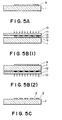
- Figures 4A - 4C illustrate another embodiment of forming a patterned optical recording layer, wherein an optical recording layer formed on a substrate is irradiated with laser light through a mask disposed in contact with the optical recording layer. More specifically, an organic film 9 formed as an optical recording layer on a substrate 1 ( Figure 4A) is irradiated with laser light 10 having a wavelength absorbable by the organic film 9 through a mask comprising a mask substrate 11 and a mask pattern 12 simultaneously over a desired area ( Figure 4B), thereby to scatter the irradiated portion to leave the masked portion as the optical recording part 3 ( Figure 4C).
- the optical recording layer can be patterned at a high resolution.
- an optical recording layer 9 on a substrate 1 can be irradiated with laser light 10 through a mask disposed with a certain spacing 17 from the optical recording layer 9 ( Figure 5B(1)) or through a mask disposed in contact with a side of the substrate 1 opposite to the side on which the optical recording layer 9 is formed.
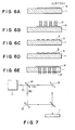
- Figures 6A - 6E show another embodiment of the process for producing an optical recording medium having a patterned optical recording layer on a substrate.
- an organic film 9 formed on a substrate 1 is irradiated with laser light 10 having a wavelength absorbable by the organic film and patterned in stripes according to an optical interference method (Figure 6B), thereby to scatter the irradiated portion to form tracking grooves 2 and leave the masked portion as an optical recording part 3 ( Figure 6C).
- the width of scattering of the irradiated portion of the organic film is determined depending on the intensity of the laser light and the sensitivity of the organic film.
- the pattern formation according to the optical interference method in the present invention may be effected by means of various optical systems.
- Figure 7 illustrates an example of such a system for interference of laser light.
- laser light 10 emitted from a laser source 11 is split by means of a half mirror (beam splitter) 12 into two fluxes along optical paths A and B.
- the fluxes A and B are then respectively reflected by mirrors 13 and then incident on a recording layer (not shown) on a substrate 1, where interference fringes are formed due to interference between the two fluxes.
- the angle of intersection of the fluxes A and B can be varied by changing the angles of the mirrors 13, so that the pitch of the interference fringes formed on the recording layer is changed. More specifically, the pitch of the interference fringes is determined by the angles of incidence of the fluxes A and B on the substrate 1 and can be controlled as desired.
- the light intensity distribution of the interference fringes forms a sine curve.
- the portions of the optical recording layer receiving a photo-energy exceeding a certain level required for scattering are determined by intersections of the sine curve and the energy level.
- the line width i.e., the width of the tracking groove, is governed by the intensity distribution of the interference fringes given by the laser energy.
- the groove in the case of the groove (concavity) retaining an organic film, the groove itself can be used as an optical recording part and the convex portion of the optical recording layer can be used as a tracking guide by utilizing a phase difference.
- a base member 5 is applied on the optical recording layer 3 by the medium of an adhesive layer 4 to form an optical recording medium as shown in Figure 1 or Figure 2 according to the present invention.
- an organic film 9 on a substrate 1 ( Figure 8A), bond it to a base 5 by the medium of an adhesive layer 4 ( Figure 8B) and then apply the above-mentioned various methods of irradiation of the organic film 9 with laser light 10 for providing a patterned optical recording layer on the substrate 1 as shown in Figures 8C(1) - 8C(3).
- the organic film 9 may preferably comprise a material compatible with light for use optical recording and reproduction.
- the organic film 9 should preferably form pits as parts for recording data bits providing a large difference in reflectivity from that of un-recorded parts.
- the organic film 9 is required to show absorption in the above-mentioned range.
- the organic film 9 causes a change in reflectivity at a low energy irradiation for recording. It is further preferred that the organic film 9 does not readily cause a change in reflectivity at recording parts (pits, etc.) or unrecorded parts.
- the material constituting the organic film 9 may preferably form a solution or a dispersion adapted for continuous application in view of the productivity of the recording medium.
- Examples of such a material for organic film 9 may include: anthraquinone derivatives (particularly those having an indanthrene skeleton), dioxadine and its derivatives, triphenodithiazine compounds, phenanthrene derivatives, cyanine compounds, merocyanine compounds, pyrylium compounds, xanthine compounds, triphenylmethane compounds, croconium dyes, azo dyes, crocones, azines, indigoids, methine dyes, azulenes, squarium derivatives, sulfide dyes, and metal dithiolate complexes.
- anthraquinone derivatives particularly those having an indanthrene skeleton
- dioxadine and its derivatives triphenodithiazine compounds
- phenanthrene derivatives cyanine compounds
- merocyanine compounds pyrylium compounds
- xanthine compounds triphenylmethane compounds
- Such a dye or colorant as described above can be used alone or mixed with an agent for quenching the dye in the excited state to form a dye composition.
- the quenching agent may be selected from the examples thereof described hereinbelow in consideration of the compatibility or solubility with the dye and the solvent.
- the quencher may be added in several wt. % to 50 wt. % of the dye. Too little quencher fails to show its effect sufficiently, and the addition in excess of 50 wt. % can lead to a decrease in sensitivity. For these reasons, it is preferred to use the quencher in a proportion of 10 wt. % to 30 wt. %, particularly around 20 wt. %, of the dye.
- the quencher may include various metal chelate compounds, such as four coordination-type compounds having central atoms such as Zn, Cu, Ni, Cr, Co, Mn, Pd and Zr with polydentate ligands inclusive of tetra-dentate ligands such as N4, N2O2, N2S2, S4, O2S2 and O4; a combination of tri-dentate ligands such as NS2, O3 and NOS with another ligand such as water, ammonia, halogen, phosphine, amine, arsine and olefin; or combination of bidentate ligands such as N2, NO, O2 and S2; biscyclopentadienyl ligand, cyclopentadienyl-tropylinium ligand; or combination of the above.
- metal chelate compounds such as four coordination-type compounds having central atoms such as Zn, Cu, Ni, Cr, Co, Mn, Pd and Zr with polyden
- quencher may further include various aromatic amines or diamines, nitrogen-containing aromatic compounds and their onium salts, such as aminium salt; diimmonium salt, pyridinium salt and quinolynium salt.
- the quencher may further be a pyrylium salt which is a salt of an oxygen-containing aromatic compound.
- the dye or its composition can be used in combination with a binder wherein the dye is contained in a dispersion or an amorphous state (solid solution).
- the binder may be selected from a wide variety of resins.
- binder may include cellulose esters such as nitrocellulose, cellulose phosphate, cellulose sulfate, cellulose acetate, cellulose propionate, cellulose butyrate, cellulose myristate, cellulose palmitate, cellulose acetate propionate, and cellulose acetate butyrate; cellulose ethers, such as methyl cellulose, ethyl cellulose, propyl cellulose, and butyl cellulose; vinyl resins, such as polystyrene, polyvinyl chloride, polyvinyl acetate, polyvinyl butyral, polyvinyl acetal, polyvinyl alcohol, and polyvinylpyrrolidone; copolymer resins, such as styrene-butadiene copolymer, styrene-acrylonitrile copolymer, styrene-butadiene-acrylonitrile copolymer, and vinyl chloride-vinyl acetate copolymer, and
- Such a binder resin may preferably be used in a proportion of 10 - 90 wt. %, particularly 30 - 80 wt. %, of the dye or its composition.
- the dye or its composition may be dissolved in an organic solvent to form a coating composition.
- organic solvent to be used can be different depending on the dye used, the kind of the binder when used, or whether the dye is contained in the binder in the form of a dispersion or amorphous state.
- examples of the organic solvent generally used for this purpose may include: alcohols, such as methanol, ethanol and isopropanols; ketones, such as acetone, methyl ethyl ketone and cyclohexanone; amides, such as N,N-dimethylformamide, and N,N-dimethylacetoamide; sulfoxides, such as dimethyl sulfoxide; ethers, such as tetrahydrofuran, dioxane, ethylene glycol monomethyl ether; esters, such as methyl acetate, ethyl acetate, and butyl acetate; aliphatic halogenated hydrocarbons, such as chloroform, methylene chloride, dichloroethylene, carbon tetrachloride, and trichloroethylene; and aromatic compounds, such as benzene, toluene, xylene, ligroin, monochlorobenzene, and dichlorobenzen
- the organic film 9 of such a dye or its composition may be formed by a known coating method, such as dip coating, spray coating, spinner coating, bar coating, roller coating, blade coating and curtain-flow coating from a coating composition as described above.
- the thickness of the organic film may generally be 500 - 2000 ⁇ , preferably around 1000 ⁇ . More specifically, a rather thin film is preferred in respect of the recording sensitivity and a rather thick film is preferred in respect of the reproduction S/N ratio. The optimum thickness can vary to some extent depending on the material for the organic film used.
- the base member 5 for protection and easiness of handling may be composed of any material which has been used for such purpose, particularly for constituting a card base.
- a material may include: polyvinyl chloride, vinyl chloride-vinyl acetate copolymer, polyvinylidene chloride, acrylic polymers such as polymethyl methacrylate, polystyrene, polypropylene, polycarbonate, epoxy resin, and acrylonitrilebutadiene-styrene copolymer.
- a sheet of metal such as iron, stainless steel, aluminum, tin, copper or zinc, synthetic or natural paper, etc. can be used for the base member 5. It is further possible to use a laminate of the above materials.
- the base member 5 may be subjected to a pretreatment for improvement of adhesiveness, such as corona discharge treatment, plasma treatment, and primer coating.
- the adhesive layer 4 may for example be composed of a hot melt-type resin, such as ethylene-vinyl acetate copolymer, ethylene-ethyl acrylate copolymer, vinyl acetate-acrylate copolymer, and polyimide resin.
- Thermocuring type, photocuring type or photo-thermal-curing type adhesive can deteriorate the optical recording layer 4 and is not suitably be applied entirely over the optical recording layer 4 for entire surface bonding but can be used for local bonding or for entire surface bonding after the optical recording layer has been coated with a protective film.
- the adhesive can be a known one and need not be particularly limited.
- the laser light 10 may have different wavelengths depending on the source but the wavelength is required to be absorbable by the optical recording layer 4. Further, the laser light 10 should preferably have a short wavelength, be capable of irradiating a large area and have a uniform energy.
- Preferred examples of the laser light source include excimer lasers containing XeF (351 nm), N2 (337 nm), XeCl (308 nm), KrF (248 nm), KrCl (222 nm), ArF (193 nm), etc.
- tracking groove width it is also possible to use a semiconductor laser, a CO2 laser, a YAG laser, etc., after condensing the beam spot to a desired diameter (tracking groove width).
- the mask substrate 11 constituting a mask as shown in Figures 4B, 5B and 8C(2) may comprise a material having a high transmittance with respect to the laser light used, thus not absorbing the laser light.
- the substrate 11 can comprise either an organic or inorganic material.
- the organic material may for example be acrylic resin, polyester, imide resin and polycarbonate.
- the inorganic material may for example be quartz glass, blue plate glass or silicon substrate.
- the masking member or film 12 may preferably comprise a material absorbing the laser light used, thus showing little transmittance to the laser light.
- a material may include Cr, Ni, Al, TiN and NiCr. It is possible to increase the resolving power by forming a reflection preventing layer on the masking film.
- the optical recording layer comprising an organic film is provided with a tracking groove without using a stamper.
- the optical recording layer is formed on a flat substrate, so that it is formed in a uniform thickness, thus providing a stable recording sensitivity.
- the tracking groove thus obtained provides a high reflective contrast (as defined hereinbefore) relative to the optical recording part, thus allowing stable tracking.
- a 0.4 mm-thick substrate of polymethyl methacrylate (hereinafter abbreviated as "PMMA") was coated with a coating solution of 2.7 wt. parts of a polymethine compound, 1,1,5,5-tetrakis(p-diethylaminophenyl)-2,4-pentadienium perchlorate, in 97.3 wt. parts of diacetone alcohol by the direct gravure process, followed by drying to form an about 900 ⁇ -thick organic film as an optical recording layer.
- PMMA polymethyl methacrylate
- the optical recording layer was irradiated with KrF laser light through a mask disposed in contact with the optical recording layer as shown in Figure 4B.
- the mask used at this time was one comprising a Cr masking film on a quartz substrate.
- the laser power was about 170 mJ for an area of 5 mm ⁇ 30 mm and a distance of 300 mm.
- the portion of the optical recording layer irradiated with the laser light was scattered to form a pattern including a 2.5 ⁇ m-wide tracking groove and a 9.5 ⁇ m-wide optical recording part.
- a 0.3 mm-thick PMMA base sheet or film was applied by the medium of a 0.05 mm-thick thermoplastic adhesive layer of ethylene-vinyl acetate copolymer on the optical recording layer provided with the tracking groove to obtain an optical recording medium.
- the optical recording medium was subjected to data writing by using a semiconductor laser with an oscillation frequency of 830 nm to illuminate the optical recording part with spot of 1.5 ⁇ m diameter through the substrate at a recording power of 6 mW and a recording frequency of 2 MHz. Then, the recorded data were reproduced at a reading power of 0.8 mW and the reproduction waveform was subjected to spectrum analysis (scanning filter band width 30 KHz), whereby the C/N ratio was measured to be 0.54.
- the tracking groove and the optical recording part showed reflectivities of about 5 % and 15 %, respectively, with respect to the reproduction laser light. Further, the tracking groove and the optical recording part gave a reflective contrast of 0.65, thus providing a sufficiently accurate tracking signal.
- a 0.4 mm-thick PMMA substrate was coated with a coating solution of 2.7 wt. parts of the same polymethine compound as used in Example 1 in 97.3 wt. parts of diacetone alcohol by the direct gravure process, followed by drying to form an about 900 ⁇ -thick organic film as an optical recording layer.
- the optical recording layer was irradiated with KrF laser light through a mask disposed with a spacing of 10 ⁇ m from the optical recording layer as shown in Figure 5B(1).
- the mask used at this time was one comprising a Cr masking film on a quartz substrate and disposed so that the Cr film faced the optical recording layer.
- the laser power was about 170 mJ for an area of 5 mm ⁇ 30 mm and a distance of 300 mm.
- the portion of the optical recording layer irradiated with the laser light was scattered to form a pattern including a 2.5 ⁇ m-wide tracking groove and a 9.5 ⁇ m-wide optical recording part.
- a 0.3 mm-thick PMMA base sheet was applied by the medium of a 0.05 mm-thick thermoplastic adhesive layer of ethylene-vinyl acetate on the optical recording layer provided with the tracking groove to obtain an optical recording medium.
- the optical recording medium was subjected to data writing by using a semiconductor laser with an oscillation frequency of 830 nm to illuminate the optical recording part with a spot of 1.5 ⁇ m diameter through the substrate at a recording power of 6 mW and a recording frequency of 2 MHZ. Then, the recorded data were reproduced at a reading power of 0.8 mW and the reproduction waveform was subjected to spectrum analysis (scanning filter band width 30 KHz), whereby the C/N ratio was measured to be 0.52.
- the tracking groove and the optical recording part gave a reflective contrast of 0.64, thus providing a sufficiently accurate tracking signal.
- a 0.4 mm-thick PMMA substrate was coated with a coating solution of 3 wt. parts of the same polymethine compound as used in Example 1 in 97 wt. parts of dichloroethane by spinner coating, followed by drying to form an about 1000 ⁇ -thick organic film as an optical recording layer.
- the optical recording layer was irradiated with interference fringes of ArF laser light having a wavelength of 193 nm and having passed through an interference system as shown in Figure 7.
- the laser power at this time was about 170 mJ/30 cm for an area of 5 mm ⁇ 30 mm.
- a pattern with grooves of 2.5 ⁇ m in width and 12 ⁇ m in spacing between adjacent grooves was formed on the substrate.
- a 0.3 mm-thick PMMA base sheet was applied by the medium of a 0.05 mm-thick thermoplastic adhesive layer of ethylene-vinyl acetate copolymer on the optical recording layer provided with the tracking groove to obtain an optical recording medium.
- the optical recording medium was subjected to data writing by using a semiconductor laser with an oscillation frequency of 830 nm to illuminate the optical recording part with a spot of 1.5 ⁇ m diameter through the substrate at a recording power of 6 mW and a recording frequency of 2 MHz. Then, the recorded data were reproduced at a reading power of 0.8 mW and the reproduction waveform was subjected to spectrum analysis (scanning filter band width 30 KHz), whereby the C/N ratio was measured to be 0.5. Further, the tracking groove and the optical recording part gave a reflective contrast of 0.69, thus providing a sufficiently accurate tracking signal.
- a 0.4 mm-thick PMMA substrate was coated with a coating solution of 6 wt. parts of the same polymethine compound as used in Example 1 in 94 wt. parts of diacetone alcohol by roller coating, followed by drying to form an about 2000 ⁇ -thick organic film as an optical recording layer.
- the optical recording layer was irradiated with one shot of interference fringes of KrF laser light having a wavelength of 248 nm and having passed through an interference system as shown in Figure 7.
- the laser power was about 120 mJ/30 cm for an area of 5 mm ⁇ 30 mm.
- a optical recording layer pattern with grooves of 2.5 ⁇ m in width, 12 ⁇ m in spacing and 1000 ⁇ in depth was formed on the substrate.
- the substrate with the optical recording layer pattern was formed into an optical recording medium, and subjected to recording and reproduction tests in the same manner as in Example 1, whereby a C/N ratio of 0.55 was obtained.
- the optical recording part and the tracking groove gave a difference in height of about 1000 ⁇ , and the ratio R(d2)/R(d1) was 0.5. Further, the optical recording part and the tracking groove showed a reflective contrast of 0.51.
Landscapes
- Engineering & Computer Science (AREA)
- Manufacturing & Machinery (AREA)
- Optical Record Carriers And Manufacture Thereof (AREA)
- Thermal Transfer Or Thermal Recording In General (AREA)
Applications Claiming Priority (8)
| Application Number | Priority Date | Filing Date | Title |
|---|---|---|---|
| JP92087/87 | 1987-04-16 | ||
| JP9208787 | 1987-04-16 | ||
| JP101814/87 | 1987-04-27 | ||
| JP10181487 | 1987-04-27 | ||
| JP104676/87 | 1987-04-30 | ||
| JP62104676A JP2754204B2 (ja) | 1987-04-30 | 1987-04-30 | 光記録媒体の製造方法 |
| JP140083/87 | 1987-06-05 | ||
| JP14008387 | 1987-06-05 |
Publications (3)
| Publication Number | Publication Date |
|---|---|
| EP0287394A2 true EP0287394A2 (de) | 1988-10-19 |
| EP0287394A3 EP0287394A3 (en) | 1989-02-22 |
| EP0287394B1 EP0287394B1 (de) | 1994-03-02 |
Family
ID=27467996
Family Applications (1)
| Application Number | Title | Priority Date | Filing Date |
|---|---|---|---|
| EP88303428A Expired - Lifetime EP0287394B1 (de) | 1987-04-16 | 1988-04-15 | Verfahren zur Herstellung von einem optischen Datenträger |
Country Status (2)
| Country | Link |
|---|---|
| EP (1) | EP0287394B1 (de) |
| DE (1) | DE3888006T2 (de) |
Cited By (1)
| Publication number | Priority date | Publication date | Assignee | Title |
|---|---|---|---|---|
| EP1047055A1 (de) * | 1999-04-22 | 2000-10-25 | 3M Innovative Properties Company | Optisches Speichermedium |
Family Cites Families (4)
| Publication number | Priority date | Publication date | Assignee | Title |
|---|---|---|---|---|
| FR2214934B1 (de) * | 1973-01-18 | 1978-03-24 | Thomson Csf | |
| FR2368779A1 (fr) * | 1976-10-22 | 1978-05-19 | Thomson Brandt | Support thermosensible destine a l'enregistrement d'information et procede d'enregistrement d'information sur un tel support |
| EP0072854A4 (de) * | 1981-02-27 | 1986-01-14 | Drexler Tech | Bankkarte für automatische schaltermaschinen und dergleichen. |
| JPS5965951A (ja) * | 1982-10-08 | 1984-04-14 | Toshiba Corp | 情報記憶媒体用原盤 |
-
1988
- 1988-04-15 EP EP88303428A patent/EP0287394B1/de not_active Expired - Lifetime
- 1988-04-15 DE DE19883888006 patent/DE3888006T2/de not_active Expired - Fee Related
Cited By (3)
| Publication number | Priority date | Publication date | Assignee | Title |
|---|---|---|---|---|
| EP1047055A1 (de) * | 1999-04-22 | 2000-10-25 | 3M Innovative Properties Company | Optisches Speichermedium |
| WO2000065586A1 (en) * | 1999-04-22 | 2000-11-02 | 3M Innovative Properties Company | Optical storage medium |
| WO2000065409A3 (en) * | 1999-04-22 | 2001-04-05 | 3M Innovative Properties Co | Optical storage medium |
Also Published As
| Publication number | Publication date |
|---|---|
| DE3888006D1 (de) | 1994-04-07 |
| EP0287394B1 (de) | 1994-03-02 |
| DE3888006T2 (de) | 1994-07-21 |
| EP0287394A3 (en) | 1989-02-22 |
Similar Documents
| Publication | Publication Date | Title |
|---|---|---|
| US4954380A (en) | Optical recording medium and process for production thereof | |
| US4965153A (en) | Optical recording medium | |
| JP2553860B2 (ja) | 光記録部材及びその製造方法並びに光記録カ−ドの製造方法 | |
| US5009818A (en) | Method of manufacturing an optical information recorded disc | |
| US5738973A (en) | Optical information recording medium | |
| EP0280531A2 (de) | Optischer Datenaufzeichnungsträger | |
| US5904969A (en) | Optical data recording medium and manufacturing method thereof | |
| US5248990A (en) | Process for producing optical recording medium for optical data recording and reproduction | |
| US5246758A (en) | Optical recording medium | |
| US5370970A (en) | Write-once-read-many optical disk | |
| EP0287394B1 (de) | Verfahren zur Herstellung von einem optischen Datenträger | |
| US5264327A (en) | Method for preparing information recording medium | |
| EP0475529A1 (de) | Optisches Aufzeichnungselement | |
| EP0259151B1 (de) | Optische Karte und Verfahren zu ihrer Herstellung | |
| JP2531738B2 (ja) | 光記録媒体の製造方法及び情報記録方法 | |
| JP2754204B2 (ja) | 光記録媒体の製造方法 | |
| US5413893A (en) | Optical information recording medium | |
| JP2512042B2 (ja) | 光記録媒体および光記録方法 | |
| JP2556351B2 (ja) | 光記録媒体およびその製造方法 | |
| JPH01158640A (ja) | 光ディスクの製造方法 | |
| JPS63121143A (ja) | 光カ−ドおよびその製造方法 | |
| JP2512043B2 (ja) | 光記録媒体及び光記録方法 | |
| JPH01287843A (ja) | 光記録媒体及びその製造方法 | |
| JPH06333267A (ja) | 光記録媒体およびその製造方法 | |
| JP2517645B2 (ja) | 光記録媒体 |
Legal Events
| Date | Code | Title | Description |
|---|---|---|---|
| PUAI | Public reference made under article 153(3) epc to a published international application that has entered the european phase |
Free format text: ORIGINAL CODE: 0009012 |
|
| AK | Designated contracting states |
Kind code of ref document: A2 Designated state(s): DE FR GB IT |
|
| PUAL | Search report despatched |
Free format text: ORIGINAL CODE: 0009013 |
|
| AK | Designated contracting states |
Kind code of ref document: A3 Designated state(s): DE FR GB IT |
|
| 17P | Request for examination filed |
Effective date: 19890726 |
|
| 17Q | First examination report despatched |
Effective date: 19901206 |
|
| ITTA | It: last paid annual fee | ||
| GRAA | (expected) grant |
Free format text: ORIGINAL CODE: 0009210 |
|
| AK | Designated contracting states |
Kind code of ref document: B1 Designated state(s): DE FR GB IT |
|
| PG25 | Lapsed in a contracting state [announced via postgrant information from national office to epo] |
Ref country code: FR Free format text: THE PATENT HAS BEEN ANNULLED BY A DECISION OF A NATIONAL AUTHORITY Effective date: 19940302 |
|
| REF | Corresponds to: |
Ref document number: 3888006 Country of ref document: DE Date of ref document: 19940407 |
|
| ITF | It: translation for a ep patent filed | ||
| EN | Fr: translation not filed | ||
| PLBE | No opposition filed within time limit |
Free format text: ORIGINAL CODE: 0009261 |
|
| STAA | Information on the status of an ep patent application or granted ep patent |
Free format text: STATUS: NO OPPOSITION FILED WITHIN TIME LIMIT |
|
| 26N | No opposition filed | ||
| REG | Reference to a national code |
Ref country code: GB Ref legal event code: IF02 |
|
| PGFP | Annual fee paid to national office [announced via postgrant information from national office to epo] |
Ref country code: GB Payment date: 20030401 Year of fee payment: 16 |
|
| PGFP | Annual fee paid to national office [announced via postgrant information from national office to epo] |
Ref country code: DE Payment date: 20030424 Year of fee payment: 16 |
|
| PG25 | Lapsed in a contracting state [announced via postgrant information from national office to epo] |
Ref country code: GB Free format text: LAPSE BECAUSE OF NON-PAYMENT OF DUE FEES Effective date: 20040415 |
|
| PG25 | Lapsed in a contracting state [announced via postgrant information from national office to epo] |
Ref country code: DE Free format text: LAPSE BECAUSE OF NON-PAYMENT OF DUE FEES Effective date: 20041103 |
|
| GBPC | Gb: european patent ceased through non-payment of renewal fee |
Effective date: 20040415 |
|
| PG25 | Lapsed in a contracting state [announced via postgrant information from national office to epo] |
Ref country code: IT Free format text: LAPSE BECAUSE OF NON-PAYMENT OF DUE FEES;WARNING: LAPSES OF ITALIAN PATENTS WITH EFFECTIVE DATE BEFORE 2007 MAY HAVE OCCURRED AT ANY TIME BEFORE 2007. THE CORRECT EFFECTIVE DATE MAY BE DIFFERENT FROM THE ONE RECORDED. Effective date: 20050415 |