EP0280802A1 - Génération des signaux de déclechement - Google Patents
Génération des signaux de déclechement Download PDFInfo
- Publication number
- EP0280802A1 EP0280802A1 EP87301917A EP87301917A EP0280802A1 EP 0280802 A1 EP0280802 A1 EP 0280802A1 EP 87301917 A EP87301917 A EP 87301917A EP 87301917 A EP87301917 A EP 87301917A EP 0280802 A1 EP0280802 A1 EP 0280802A1
- Authority
- EP
- European Patent Office
- Prior art keywords
- stream
- cycle
- parallel
- signal
- bits
- Prior art date
- Legal status (The legal status is an assumption and is not a legal conclusion. Google has not performed a legal analysis and makes no representation as to the accuracy of the status listed.)
- Granted
Links
- 101150071746 Pbsn gene Proteins 0.000 claims abstract description 24
- 238000000034 method Methods 0.000 claims description 9
- 230000003111 delayed effect Effects 0.000 description 4
- 238000010586 diagram Methods 0.000 description 4
- 230000003247 decreasing effect Effects 0.000 description 1
- 238000001514 detection method Methods 0.000 description 1
- 230000007274 generation of a signal involved in cell-cell signaling Effects 0.000 description 1
- 230000001360 synchronised effect Effects 0.000 description 1
Images
Classifications
-
- H—ELECTRICITY
- H03—ELECTRONIC CIRCUITRY
- H03K—PULSE TECHNIQUE
- H03K3/00—Circuits for generating electric pulses; Monostable, bistable or multistable circuits
- H03K3/84—Generating pulses having a predetermined statistical distribution of a parameter, e.g. random pulse generators
Definitions
- This invention relates to the generation of trigger signals for a serial stream of bits which has a continuously repeating pattern and which has been formed by serialising a plurality of parallel streams.
- the invention has particular, but not exclusive, application to the generation of trigger signals for a class of serial streams known as 'maximal length Pseudo Random Binary Sequences' (hereinafter referred to as PRBS), which may be formed by serialising a plurality of parallel streams.
- PRBS 'maximal length Pseudo Random Binary Sequences'
- bit rate of a serial stream formed as above is typically an order of magnitude higher than that of the parallel streams from which it is formed.
- Such serial streams are used, for example, in the testing of high speed digital signal links.
- One way of producing such a trigger signal would be to sense a particular sequence of bits in the serial stream. This would require logic circuitry operating at the high (serial) rate, and would be complex.
- the present invention is concerned with a technique which will produce a trigger signal on every pattern cycle and which can be implemented with circuitry operating mainly at the lower (parrallel clock rate.
- apparatus for generating trigger signals for a serial stream of bits which has a continuously repeating pattern and which has been formed by serialising a plurality of parallel streams said apparatus being chracterised by comprising means for sensing within which parallel stream cycle a trigger signal should occur and means for sensing with which bit of the parallel stream in that cycle that trigger signal should be associated.
- a method for generating trigger signals for a serial stream of bits which has a continuously repeating pattern and which has been formed by serialising a plurality of parallel streams the method being characterised by the steps of sensing within which parallel stream cycle a trigger signal should occur and sensing with which bit of the parallel stream in that cycle the trigger signal should be associated.
- the method has application generally to the generation of trigger signals for use with parallel word generators whose outputs are serialised to form a bit stream at a higher rate.
- the invention will be described in two stages. Firstly the generation of trigger signals for the general case of a pattern of length P formed by serialising W parallel streams is briefly considered. Secondly the more particular case of trigger signal generation for high rate PRBS sequences formed by serialising a plurality of parallel streams will be considered in detail.
- PRBS signals are commonly used for testing digital signal links.
- a PRBS is generated using a multi-stage shift register by combining selected outputs of the shift register by modulo 2 addition and feeding back the resulting signal as input to the first stage.
- the output of any stage of the shift register provides a maximal length PRBS provided the feedback connections are appropriately made (maximum length is 2 n - 1 for an N stage register).
- maximum length is 2 n - 1 for an N stage register.
- PRBS's may be generated using the series-parallel technique which can be found in the literature (eg) 'Series-parallel generation of m-sequences' by J. J. O'Reilly, The Radio and Electronic Engineer, vol 45, no. 4, pp171-176, April 1975). This document describes how to generate parallel streams which when serialised will form a PRBS.
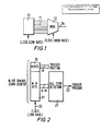
- FIG. 1 there is shown in block diagram form an arrangement for producing a higher rate PRBS.
- the block 10 contains means for producing a plurality of streams on lines 11, such means being drived from the series-parallel technique described in the abovementioned document and operating at the lower rate.
- the streams on lines 11 are serialised by a multiplexer 12 to produce a higher rate PRBS on line 14.
- the number of parallel lines 11 is usually chosen to be a power of 2 to simplify implementation of the serialiser 12 in binary logic circuits.
- the trigger signal must be related to one particular bit in the serial output stream and must repeat its self at that bit for each successive repetition of the output PRBS :- ie at a spacing of 2 N - 1 bits.
- One property of a 2 N - 1 PRBS is that any sequence of N bits occurs only once during each pattern repetition. Therefore one way of producing a trigger signal would be to provide some means for detecting a sequence of N bits in the serial stream, and to generate the trigger signal on recognition of such sequence. Such means would have to operate at the high rate and would be complicated to construct. It is clearly preferable if the trigger signal can be generated with equipment operating mostly at the lower rate, and this is achived with embodiments according to the present invention.
- the first embodiment is shown in Fig. 2 of the drawings. It comprises an N stage binary counter, where 2 N - 1 is the PRBS to be generated. If 2 m parallel streams are used to generate this PRBS, then the counter can be considered to consist of two sections. A first section 17 contains the N-m least significant bits, and a second section 18 consists of the m most significant bits.
- the counter is clocked by a clock signal on line 20 at the low (parallel) rate, and is arranged to count downwards with a cycle length of 2 N - 1 - ie one count state (say the all 1's state) is skipped.
- Block 21 detects an all 0's condition in the lower N-m counter bits, and gives an output on line 22. These conditions occur every 2 (N-m) clock cycles, except where the all 1's state is skipped when the spacing is 2 (N-m) - 1 clock cycles.
- the upper m bits, section 18, considered alone will cycle through a count of 2 m - 1 down to 0, with the change from 0 back to 2 m - 1 occuring where the spacing between successive signals on line 22 is 2 (N-m) -1.
- Signals on line 22 may be used to indicate the clock cycles during which trigger signals should ocur and the upper m bits used to determine thei high rate bit with which that trigger signal shoud be associted.
- the spacing between trigger signals in the serial output is either:- (i) 2 (N-m) x 2 m - 1 cycles x bits/cycle -1 (due to decreasing m bit count) or (ii) [2 (N-m) - 1] x 2 m + 2 m - 1 cycles x bits/cycle + (due to increase in m bit count).
- the spacing is 2 N - 1 serial bits as required. It should be noted for this embodiment that the point in the output stream at which the trigger signal occurs can be defined by controlling the relationship between the starting point of the counter and the output stream.
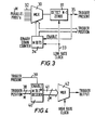
- a second embodiment for producing trigger signals is based on the proper decimation property of PRBS's, which is well known. This property dictates that if a maximal length PRBS is formed by serialising 2 m parallel streams, then each of the parallel streams must be a phase shifted version of the same PRBS.
- Each parallel PRBS is delayed by 2 (N-m) bits from it's predecessor except for one which must be 2 (N-m) - 1 delayed.
- Block 30 is a 2 m -to-1 multiplexer for selecting one of the parallel streams 32.
- the output of this multiplexer is sent to circuit 31 which detects a particular sequence of N bits (or N-1 zeros), and which operates at the low clock rate.
- An m-bit down counter 34 is used to control parallel stream selection in the multiplexer. This counter is enabled for one count when the output of the detection circuit on line 35 is active, thus selecting the next stream.
- output pulses are generally obtained from circuit 31 at intervals of 2 (N-m) low rate clock cycles, but one pulse in every 2 m is spaced by 2 (N-m) -1 low rate cycles from it's predecessor. Each such pulse identifies a low rate cycle in which a trigger signal should occur.
- the high rate bit within these cycles with which the trigger signal should be associated is defined by the m bits from counter 34.
- the information generated by this embodiment is equivalent to that generated by the first embodiment shown in Fig. 2, and so trigger signals are produced every 2 N -1 high rate bits.
- the information produced by the circuits of Figs. 2 and 3, (viz. the identifying of cycles, and positions within those cycles, when trigger signals should occur), can be ued to generate a high rate trigger signal output using one of several posible schemes.
- Block 40 is an m-to-2 m decoder which is enabled by the 'trigger present' signal on line 39, and whose selection inputs are fed from the m 'trigger position' outputs from the previous embodiments.
- This decoder operates at the low rate. When not enabled all decoder outputs 41 are say at logic 0.
- the outputs 41 are serialised by multiplexer 42 to form the high rate trigger signal.
- This multiplexer is identical to the multiplexer used to form the high rate data stream (Fig. 1) thus minimising the circuit types required to operate at the high rate.
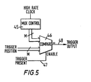
- FIG. 5 An alternative shceme for generating the trigger signal is shown in fig. 5 of the drawings.
- This scheme requires extra circuitry in the high speed data mux.
- circuitry shown at 45 which cycles through 2 m states in order to control gating of 2 m inputs to a single output. It is possible to arrange for comparison of these states with the trigger position signals to generate the correct high rate trigger output.
- This comparison can be carried by the block shown schematically at 46 which is enabled only during those cycles when a trigger signal should occur, by the 'trigger present' signal on line 47.
- the required trigger signal appears on line 48.
Landscapes
- Synchronisation In Digital Transmission Systems (AREA)
- Compression, Expansion, Code Conversion, And Decoders (AREA)
- Selective Calling Equipment (AREA)
Priority Applications (4)
| Application Number | Priority Date | Filing Date | Title |
|---|---|---|---|
| EP87301917A EP0280802B1 (fr) | 1987-03-05 | 1987-03-05 | Génération des signaux de déclechement |
| DE8787301917T DE3773369D1 (de) | 1987-03-05 | 1987-03-05 | Erzeugung von triggersignalen. |
| US07/164,045 US4998263A (en) | 1987-03-05 | 1988-03-04 | Generation of trigger signals |
| JP63052026A JPS63253714A (ja) | 1987-03-05 | 1988-03-04 | トリガ信号発生器 |
Applications Claiming Priority (1)
| Application Number | Priority Date | Filing Date | Title |
|---|---|---|---|
| EP87301917A EP0280802B1 (fr) | 1987-03-05 | 1987-03-05 | Génération des signaux de déclechement |
Publications (2)
| Publication Number | Publication Date |
|---|---|
| EP0280802A1 true EP0280802A1 (fr) | 1988-09-07 |
| EP0280802B1 EP0280802B1 (fr) | 1991-09-25 |
Family
ID=8197807
Family Applications (1)
| Application Number | Title | Priority Date | Filing Date |
|---|---|---|---|
| EP87301917A Expired EP0280802B1 (fr) | 1987-03-05 | 1987-03-05 | Génération des signaux de déclechement |
Country Status (4)
| Country | Link |
|---|---|
| US (1) | US4998263A (fr) |
| EP (1) | EP0280802B1 (fr) |
| JP (1) | JPS63253714A (fr) |
| DE (1) | DE3773369D1 (fr) |
Families Citing this family (6)
| Publication number | Priority date | Publication date | Assignee | Title |
|---|---|---|---|---|
| US5187676A (en) * | 1991-06-28 | 1993-02-16 | Digital Equipment Corporation | High-speed pseudo-random number generator and method for generating same |
| US5639451A (en) * | 1995-06-07 | 1997-06-17 | Roy M. Evans, Jr. | Hair treatment compositions |
| JP3501731B2 (ja) * | 2000-06-19 | 2004-03-02 | 日本電気株式会社 | 光デジタル伝送装置の固定パタン送信防止回路 |
| JP2003249923A (ja) * | 2002-02-25 | 2003-09-05 | Ando Electric Co Ltd | ビットエラー測定装置及びそのトリガー信号発生回路 |
| US7219113B2 (en) * | 2003-09-26 | 2007-05-15 | International Business Machines Corporation | Pseudo-random binary sequence checker with automatic synchronization |
| JP3803664B2 (ja) * | 2003-09-30 | 2006-08-02 | 株式会社東芝 | 乱数生成回路、半導体集積回路、icカード及び情報端末機器 |
Citations (2)
| Publication number | Priority date | Publication date | Assignee | Title |
|---|---|---|---|---|
| US3881099A (en) * | 1972-12-15 | 1975-04-29 | Lannionnais Electronique | Pseudo-random binary sequence generator |
| DE2435057B2 (de) * | 1973-10-18 | 1975-09-11 | Hewlett-Packard Ltd., South Queensferry, West Lothian (Grossbritannien) | Schaltungsanordnung zum Synchronisieren und/oder erneuten Auslösen eines Generators zum Erzeugen einer Folge von pseudozufälligen Binärsignalen |
Family Cites Families (10)
| Publication number | Priority date | Publication date | Assignee | Title |
|---|---|---|---|---|
| US3648237A (en) * | 1969-02-28 | 1972-03-07 | Ibm | Apparatus and method for obtaining synchronization of a maximum length pseudorandom sequence |
| US3740478A (en) * | 1971-10-19 | 1973-06-19 | Philips Corp | Pseudo-random multiplex synchronizer |
| US3854011A (en) * | 1973-09-24 | 1974-12-10 | Gen Dynamics Corp | Frame synchronization system for digital multiplexing systems |
| FR2377729A1 (fr) * | 1977-01-14 | 1978-08-11 | Thomson Csf | Dispositif de decodage de signaux numeriques, et systeme comportant un tel dispositif |
| US4161041A (en) * | 1978-10-06 | 1979-07-10 | The United States Of America As Represented By The Secretary Of The Air Force | Pseudo random number generator apparatus |
| US4361891A (en) * | 1980-12-22 | 1982-11-30 | General Electric Company | Spread spectrum signal estimator |
| JPS60210044A (ja) * | 1984-04-03 | 1985-10-22 | Nec Corp | 誤り訂正符号送受信装置 |
| US4754465A (en) * | 1984-05-07 | 1988-06-28 | Trimble Navigation, Inc. | Global positioning system course acquisition code receiver |
| US4590601A (en) * | 1984-12-24 | 1986-05-20 | Gte Communication Systems Corporation | Pseudo random framing detector circuit |
| US4768192A (en) * | 1987-04-01 | 1988-08-30 | General Signal Corp. | Frame synchronization detection system for time division multiplexed (TDM) digital signals |
-
1987
- 1987-03-05 EP EP87301917A patent/EP0280802B1/fr not_active Expired
- 1987-03-05 DE DE8787301917T patent/DE3773369D1/de not_active Expired - Fee Related
-
1988
- 1988-03-04 US US07/164,045 patent/US4998263A/en not_active Expired - Fee Related
- 1988-03-04 JP JP63052026A patent/JPS63253714A/ja active Pending
Patent Citations (2)
| Publication number | Priority date | Publication date | Assignee | Title |
|---|---|---|---|---|
| US3881099A (en) * | 1972-12-15 | 1975-04-29 | Lannionnais Electronique | Pseudo-random binary sequence generator |
| DE2435057B2 (de) * | 1973-10-18 | 1975-09-11 | Hewlett-Packard Ltd., South Queensferry, West Lothian (Grossbritannien) | Schaltungsanordnung zum Synchronisieren und/oder erneuten Auslösen eines Generators zum Erzeugen einer Folge von pseudozufälligen Binärsignalen |
Non-Patent Citations (1)
| Title |
|---|
| THE RADIO AND ELECTRONIC ENGINEER, vol. 45, no. 4, April 1975, pages 171-176; J.J. O'REILLY "Series-parallel generation of m-sequences" * |
Also Published As
| Publication number | Publication date |
|---|---|
| EP0280802B1 (fr) | 1991-09-25 |
| JPS63253714A (ja) | 1988-10-20 |
| US4998263A (en) | 1991-03-05 |
| DE3773369D1 (de) | 1991-10-31 |
Similar Documents
| Publication | Publication Date | Title |
|---|---|---|
| US4920546A (en) | Frame synchronizing apparatus | |
| JPH04213212A (ja) | 高速パターン発生器 | |
| JPH11122117A (ja) | シリアル・パラレル変換装置 | |
| US6751639B2 (en) | Method and apparatus for generating numbers | |
| US6472913B2 (en) | Method and apparatus for data sampling | |
| JPH0146919B2 (fr) | ||
| EP0280802B1 (fr) | Génération des signaux de déclechement | |
| US20140237013A1 (en) | Pseudo-random bit sequence generator | |
| JP5171420B2 (ja) | 擬似乱数生成装置 | |
| EP1518164A1 (fr) | Procede et appareil destines a generer un nombre aleatoire au moyen de bascules metastables | |
| KR100337687B1 (ko) | 직병렬컨버터 | |
| JP4951378B2 (ja) | 波形発生器および試験装置 | |
| JP5119417B2 (ja) | 擬似乱数生成装置 | |
| US9116764B2 (en) | Balanced pseudo-random binary sequence generator | |
| JPS63245032A (ja) | 高速フレ−ム同期方式 | |
| JP2620089B2 (ja) | パターン発生装置 | |
| US5767706A (en) | Rate generator | |
| JPH09181577A (ja) | パターン発生回路 | |
| CN119210403A (zh) | 信号传送系统以及信号传送方法 | |
| JPH1185475A (ja) | 乱数発生装置 | |
| JP2003330704A (ja) | 擬似乱数パターン発生回路 | |
| JP3125651B2 (ja) | レート発生器 | |
| JPH01206718A (ja) | 乱数発生器 | |
| JPH08181577A (ja) | デジタル信号発生器 | |
| JPH0568025A (ja) | クロツク乗換回路 |
Legal Events
| Date | Code | Title | Description |
|---|---|---|---|
| PUAI | Public reference made under article 153(3) epc to a published international application that has entered the european phase |
Free format text: ORIGINAL CODE: 0009012 |
|
| AK | Designated contracting states |
Kind code of ref document: A1 Designated state(s): AT BE CH DE ES FR GB GR IT LI LU NL SE |
|
| RBV | Designated contracting states (corrected) |
Designated state(s): DE FR GB IT |
|
| 17P | Request for examination filed |
Effective date: 19890216 |
|
| 17Q | First examination report despatched |
Effective date: 19900525 |
|
| GRAA | (expected) grant |
Free format text: ORIGINAL CODE: 0009210 |
|
| AK | Designated contracting states |
Kind code of ref document: B1 Designated state(s): DE FR GB IT |
|
| REF | Corresponds to: |
Ref document number: 3773369 Country of ref document: DE Date of ref document: 19911031 |
|
| ET | Fr: translation filed | ||
| ITF | It: translation for a ep patent filed | ||
| PGFP | Annual fee paid to national office [announced via postgrant information from national office to epo] |
Ref country code: GB Payment date: 19920110 Year of fee payment: 6 |
|
| PGFP | Annual fee paid to national office [announced via postgrant information from national office to epo] |
Ref country code: FR Payment date: 19920130 Year of fee payment: 6 Ref country code: DE Payment date: 19920130 Year of fee payment: 6 |
|
| RAP2 | Party data changed (patent owner data changed or rights of a patent transferred) |
Owner name: HEWLETT PACKARD LIMITED |
|
| PLBE | No opposition filed within time limit |
Free format text: ORIGINAL CODE: 0009261 |
|
| STAA | Information on the status of an ep patent application or granted ep patent |
Free format text: STATUS: NO OPPOSITION FILED WITHIN TIME LIMIT |
|
| 26N | No opposition filed | ||
| REG | Reference to a national code |
Ref country code: FR Ref legal event code: CA |
|
| PG25 | Lapsed in a contracting state [announced via postgrant information from national office to epo] |
Ref country code: GB Effective date: 19930305 |
|
| ITPR | It: changes in ownership of a european patent |
Owner name: CAMBIO SEDE;HEWLETT - PACKARD LIMITED |
|
| GBPC | Gb: european patent ceased through non-payment of renewal fee |
Effective date: 19930305 |
|
| PG25 | Lapsed in a contracting state [announced via postgrant information from national office to epo] |
Ref country code: FR Effective date: 19931130 |
|
| PG25 | Lapsed in a contracting state [announced via postgrant information from national office to epo] |
Ref country code: DE Effective date: 19931201 |
|
| REG | Reference to a national code |
Ref country code: FR Ref legal event code: ST |
|
| PG25 | Lapsed in a contracting state [announced via postgrant information from national office to epo] |
Ref country code: IT Free format text: LAPSE BECAUSE OF NON-PAYMENT OF DUE FEES;WARNING: LAPSES OF ITALIAN PATENTS WITH EFFECTIVE DATE BEFORE 2007 MAY HAVE OCCURRED AT ANY TIME BEFORE 2007. THE CORRECT EFFECTIVE DATE MAY BE DIFFERENT FROM THE ONE RECORDED. Effective date: 20050305 |