EP0281215A2 - Programmierbare integrierte Logik-Array-Einrichtung mit verbesserter Verbindbarkeit zu Mikroprozessoren - Google Patents
Programmierbare integrierte Logik-Array-Einrichtung mit verbesserter Verbindbarkeit zu Mikroprozessoren Download PDFInfo
- Publication number
- EP0281215A2 EP0281215A2 EP88300065A EP88300065A EP0281215A2 EP 0281215 A2 EP0281215 A2 EP 0281215A2 EP 88300065 A EP88300065 A EP 88300065A EP 88300065 A EP88300065 A EP 88300065A EP 0281215 A2 EP0281215 A2 EP 0281215A2
- Authority
- EP
- European Patent Office
- Prior art keywords
- output
- signal
- bus
- input
- mode
- Prior art date
- Legal status (The legal status is an assumption and is not a legal conclusion. Google has not performed a legal analysis and makes no representation as to the accuracy of the status listed.)
- Granted
Links
Images




Classifications
-
- H—ELECTRICITY
- H03—ELECTRONIC CIRCUITRY
- H03K—PULSE TECHNIQUE
- H03K19/00—Logic circuits, i.e. having at least two inputs acting on one output; Inverting circuits
- H03K19/02—Logic circuits, i.e. having at least two inputs acting on one output; Inverting circuits using specified components
- H03K19/173—Logic circuits, i.e. having at least two inputs acting on one output; Inverting circuits using specified components using elementary logic circuits as components
- H03K19/177—Logic circuits, i.e. having at least two inputs acting on one output; Inverting circuits using specified components using elementary logic circuits as components arranged in matrix form
- H03K19/17704—Logic circuits, i.e. having at least two inputs acting on one output; Inverting circuits using specified components using elementary logic circuits as components arranged in matrix form the logic functions being realised by the interconnection of rows and columns
- H03K19/17708—Logic circuits, i.e. having at least two inputs acting on one output; Inverting circuits using specified components using elementary logic circuits as components arranged in matrix form the logic functions being realised by the interconnection of rows and columns using an AND matrix followed by an OR matrix, i.e. programmable logic arrays
- H03K19/17712—Logic circuits, i.e. having at least two inputs acting on one output; Inverting circuits using specified components using elementary logic circuits as components arranged in matrix form the logic functions being realised by the interconnection of rows and columns using an AND matrix followed by an OR matrix, i.e. programmable logic arrays one of the matrices at least being reprogrammable
Definitions
- This invention relates to programmable integrated circuit logic array devices of the type shown in Birkner et al. U.S. patent 4,124,899, issued November 7, 1978, Hartmann et al. U.S. patent 4,609,986, issued September 2, 1986, Hartmann et al. U.S. patent 4,617,479, issued October 14, 1986, Hartmann et al. U.S. patent application Serial No. 742,089, filed June 6, 1985, and Veenstra U.S. patent application Serial No. 722,684, filed April 12, 1985, all of which are hereby incorporated by reference herein, and all of which are hereinafter collectively referred to as "the patent references”.
- Prior programmable integrated circuit logic array devices have not been readily connectable to microprocessors, especially higher speed microprocessors, for certain functions.
- Various interface devices have been required in many instances between the microprocessor and the programmable logic array device.
- Prior programmable logic array devices have also not been able to completely process certain information at the basic microprocessor clock rate. This is especially of concern in relation to applications requiring faster and faster microprocessors.
- programmable integrated circuit logic array devices having one or more of the following features: (1) a bus port for receiving data directly from or making data available directly to an external microprocessor or other similar external device (hereinafter simply "microprocessor"), (2) an internal bus (preferably with internal bus arbitration logic for resolving competing demands for utilization of the bus) for conveying data between the bus port and the logic arrays and/or between the logic arrays themselves, (3) the ability to operate either in an edge-trigger mode (in which controlled functions such as input registers are triggered by the transitional edges of control signals) or in a flow-through mode (in which controlled functions such as input registers are triggered by the logical states rather than the transitional edges of the control signals), and (4) the ability to operate either in a fast mode (in which timing control signals are applied substantially directly to the elements to be controlled) or in a slow mode (in which timing signals propagate through the logic arrays rather than being
- FIG. 1 An illustrative programmable integrated circuit logic array device 10 constructed in accordance with the principles of this invention is shown in FIG. 1.
- device 10 is a device cf the general type shown in the patent references mentioned above.
- Device 10 is typically fabricated as described in the patent references, and it is ultimately made up of various elements, all of which are individually shown in the patent references and/or are individually well-known to those skilled in the art.
- device 10 is substantially symmetrical about a central vertical axis A-A as viewed in FIG. 1.
- the letter L is used in some component or signal names associated with the left side of the device, and the letter R is used in a similar way in connection with the right side of the device.
- the letters L and R are either omitted or replaced by the letter X when a name generic to the left and right sides is needed.
- the letter N is sometimes added to a signal name to indicate the logical inverse ("bar") of the signal without the N. Because of the substantially symmetrical nature of device 10, it will generally only be necessary to describe one side in detail, it being understood that the same description applies to the other side as well.
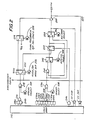
- the central elements of device 10 are the elements labelled Macrocell A and Macrocell B. Typical Macrocells A and B are shown in more detail in FIGS. 2 and 3, respectively.
- Each Macrocell A 210 or B 310 includes an erasable, electronically-programmable Logic Array 212 or 312 (labelled EPROM Array in FIG. 1) which can be programmed to perform various logic functions as shown and described, for example, in the patent references.
- Device 10 includes four A Macrocells 210 and 16 B Macrocells 310.
- the A Macrocells are somewhat simpler than the B Macrocells, and unlike the B Macrocells, are not directly connected to internal bus 20.
- VCC represents a power supply terminal or pin (typically +5 volts; logic 1).
- the next two pins are input pins, each of which is connected to a respective pair of word line drivers in each of word line driver arrays 22L and 22R.
- Each word line driver array 22 includes 40 devices, each of which drives one word line and its complementary word line in the assocaited EPROM Array as represented, for example, by the horizontal lines 40, 41, 42, etc., in FIG. 5 of U.S. patent 4,617,479).
- the signals applied to the I/P pins are general-purpose input signals which would typically come from the external microprocessor (not shown but entirely conventional) associated with device 10, or from other devices in the electronic system.
- the next pin is the inverse Write Strobe (WS bar) pin.
- the signal applied to this pin is applied (like an I/P signal) to arrays 22, and is also usable as a write strobe input signal for indicating that the microprocessor associated with device 10 is ready to write data to device 10.
- the next pin is the Clock Left (CLKL) pin.
- the signal applied to this pin is (1) applied to arrays 22 like an I/P signal, (2) optionally usable as a synchronous clock signal for the register flip-flops 230 (FIG. 2) and 330 (FIG. 3) of left side Macrocells 210 and 310, and (3) optionally usable in the Fast Output Latch Enable (Fast OLE) mode (described in detail later) to assist in timing the operation of the left side Macrocell B output latches 384.
- Fast OLE Fast Output Latch Enable
- I/O Input/Output
- I/O pins which can be used either for data input to or data output from the associated A Macrocells. In a typical application, these pins might be connected to the address or control bus of the associated microprocessor-driven system, or to other devices in the electronic system.
- the next eight pins are B Macrocell Input/Output Left and (BI/OL) pins. These are similar to the above-mentioned I/O pins, but for the associated B Macrocells. (In FIG. 3 the corresponding pin is merely labelled I/O Pin.)
- Bus Port (0-7) pins are eight Bus Port (0-7) pins. In a typical application, these pins might be connected to the data bus of the associated microprocessor-driven system for allowing byte-wide exchange of data between that external data bus and eight-conductor internal bus 20.
- VSS represents ground (0 volts; logic 0).
- BI/OR B Macrocell Input/Output Right
- I/O A Macrocell Input/Output
- the final signals to be discussed are (1) the Clock Right (CLKR) signal which is similar to the CLKL signal but for the right-hand Macrocells, (2) the inverse Read Strobe (RS bar) signal which is similar to the WS bar signal but indicates that the associated microprocessor is ready to read data from device 10, and (3) two more I/P pins similar to the previously described I/P pins.
- CLKR Clock Right
- RS bar inverse Read Strobe
- each half of device 10 includes three smaller Macrocell-type elements (collectively 24L or 24R) for respectively generating Output Latch Enable (OLE), Transfer Output to Bus (TOB), and Input Latch Enable (ILE) signals.
- OLE Output Latch Enable
- TOB Transfer Output to Bus
- ILE Input Latch Enable
- the right-hand side of device 10 also includes one more small Macrocell-type device 26 for generating a Bus Port Output Enable (BPOE) signal.
- BPOE Bus Port Output Enable
- each Bus Port pin 0-7 has a pair of tri-state driver elements 28a and 28b.
- each element 28a When enabled by the BPOE signal, each element 28a allows data to flow from an associated lead of internal bus 20 to the associated Bus Port pin.
- each element 28b When enabled by the Bus Port Input Enable (BPIE) signal, each element 28b allows data to flow from the associated Bus Port pin to an associated lead of eight-conductor internal bus 20.
- BPIE Bus Port Input Enable
- each element 28a or 28b blocks the flow of data through that element.
- FIG. 1 The other elements shown in FIG. 1 (e.g., the 16 Output Latches (O/P Latch) 384, the 16 Input ET/FT Flip-Flops 392, and the 16 multiplexers (MUX) 390) are shown again elsewhere (e.g., FIG. 3) and are more readily discussed in connection with those other drawings.
- O/P Latch 16 Output Latches
- MUX 16 multiplexers
- Macrocell 210 makes use of 11 product terms in Logic Array 212.
- Each product or P term corresponds, for example, to one vertical column 32, 34, 36, etc., in FIG. 5 of U.S. patent 4,617,479.
- the top two P terms are logically combined by AND gates 214a and 214b and OR gate 216 and (optionally) inverted by EXCLUSIVE OR gate 218 to produce an output signal which can be used either as an asynchronous clock signal for controlling regiser flip-flop 230 or for enabling tri-state driver element 260.
- Element 220 is an erasable, electronically-programmable read-only memory (EPROM) element used for controlling the "architecture" of Macrocell 210 (and therefore the architecture of device 10). Accordingly, it may be similar to the EPROM architecture control elements shown and described, for example, in U.S. patent 4,617,479 and in U.S. patent application Serial No. 742,089. (Similar EPROM architecture control elements are represented by the same schematic symbol throughout the drawings of this application.)
- EPROM electronically-programmable read-only memory
- the destination of the output signal of EXCLUSIVE OR gate 218 is controlled by multiplexer elements 222 and 224 (each of which may be similar to multiplexer elements shown and described, for example, in U.S. patent 4,617,479).
- Multiplexer 222 is controlled by ASYNC/OE Mode Bit element 226 (an EPROM element similar to element 220) and has the characteristics of a double-pole double-throw switch.
- ASYNC/OE Mode Bit element 226 an EPROM element similar to element 220
- element 226 causes multiplexer 222 to apply the output signal of gate 218 to the clock input of regiser 230 and VCC (logic 1) to multiplexer 224.
- element 226 causes multiplexer 222 to apply the Synchronous Clock signal (CLKL or CLKR in FIG.
- Multiplexer 224 is controlled by Dual Feedback O/P Tri-State element 228 (an EPROM element similar to element 220) and is like a single-pole double-throw switch. In one state (Output or O/P), element 228 causes multiplexer 224 to apply the output signal of multiplexer 222 to tri-state driver element 260 (to selectively connect the output of multiplexer 254 to the associate I/O Pin in synchronization with a logic 1 state in the output of gate 218).
- Dual Feedback O/P Tri-State element 228 an EPROM element similar to element 220
- O/P In one state (Output or O/P), element 228 causes multiplexer 224 to apply the output signal of multiplexer 222 to tri-state driver element 260 (to selectively connect the output of multiplexer 254 to the associate I/O Pin in synchronization with a logic 1 state in the output of gate 218).
- element 228 causes multiplexer 224 to apply VSS (logic 0) to driver element 260 (to interrupt the signal path between multiplexer 254 and the associateed I/O pin).
- VSS logic 0
- driver element 260 to interrupt the signal path between multiplexer 254 and the associateed I/O pin.
- the I/O pin can be used as an input through word line driver 22-262 (one portion of array 22L or 22R in FIG. 1) independent of internal feedback from multiplexer 254 through word line driver 22-258 (another portion of array 22L or 22R in FIG. 1).
- Eight other P terms in Logic Array 212 are logically combined by AND gates 232a-h and OR gate 234 and (optionally) inverted by EXCLUSIVE OR gate 236, the inversion function of which is controlled by Invert Select EPROM element 238 (similar to 220).
- the output signal of gate 236 is applied directly to the Data (D) input terminal of multiplexer 242 (similar to 224) and the Combinatorial (C) input terminal of multiplexer 254 (also similar to 224). It is also applied to EXCLUSIVE OR gate 240, together with the Q output of register 230, and the resulting signal is applied to Toggle (T) input terminal of multiplexer 242.
- Multiplexer 242 is controlled by DFF/TFF Select EPROM element 244 (similar to 220) and is like a single-pole double-throw switch. Accordingly, in one state, element 244 causes multiplexer 242 to apply the output of gate 240 to the Data (D) input terminal of register 230. (This is the Toggle, J-K or R-S flip-flop operation described in more detail in U.S. patent application Serial No. 722,684.) In the other state, element 244 causes multiplexer 242 to apply the output of gate 236 to the D input terminal of register 230. In addition to being fed back to gate 240, the Q output signal of register 230 is applied to the Register (R) input terminal of multiplexer 254.
- multiplexer 254 which is controlled by R/C Mode Select EPROM element 256 (similar to 220), can apply to its output terminal either the output signal of register 230 (i.e., a Register (R) output) or the unregisterd Combinatorial (C) output signal of gate 236.
- the resulting multiplexer 254 output signal is fed back to Logic Array 212 via word line driver array element 22-258, and it may also be applied to the associated I/O Bin via driver element 260 if that driver element is enabled as discussed above.
- the signal applied to the I/O Pin shown in FIG. 2 is applied to Logic Array 212 via word line driver array element 22-262. This signal may be either the output of driver element 260 as described immediately above, or it may be an external input signal as described in connection with FIG. 1.
- the final P term in the portion of Logic Array 212 associated with Macrocell 210 is applied to the reset (C) input terminal of register 230 via AND gate 246.
- Macrocell 210 can be programmed (element 226) to be clocked either synchronously (Synchronous Clock) or asynchronously (from the output of gate 218). It can be programmed (element 256) to produce either register (R) or combinatorial (C) output signals at the output of multiplexer 254. It can be programmed (element 228) to feed back the output of multiplexer 254 to Logic Array 212 either with or without also applying that multiplexer output to the associoated I/O Pin.
- the output of multiplexer 254 is fed back to Logic Array 212 without being applied to the associated I/O Pin, the I/O Pin remains free for use as an external input. Because the output signal of gate 218 is the logical combination of two P terms and a selective inversion (rather than being just a single P term output with no selective inversion as in prior art devices), that output signal can be a much more logically complex signal than in the past, thereby greatly enhancing the flexibility and utility of the device in relation to the generation of either an asynchronous clock signal (applied via element 222 to register 230) or an output enable signal (applied via elements 222 and 224 to element 260).
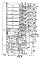
- FIG. 3 A typical B Macrocell 310 is shown in FIG. 3.
- Components of Macrocell 310 that are similar to components of Macrocell 210 have reference numbers with the same last two digits as the corresponding component of Macrocell 210.
- element 320 in FIG. 3 is similar to element 220 in FIG. 2.
- Macrocell 310 has the following components and features:
- the output signal of ASYNC/OE Mode Bit EPROM element 326 is applied to NAND gate 372.
- the other input to gate 372 is the Select Bus (SBUS) signal inverted by inverter 370.
- the SBUS signal is produced by one or two Bus I/O EPROM elements 30L or 30R (FIG. 1) for controlling, inter alia, whether the associated B Macrocell input latches are to accept data from internal bus 20 or from the associated I/O Pin.
- the output signal or NAND gate 372 is applied to AND gate 374 along with one output of multiplexer 322.
- the output signal of multiplexer 354 is not necessarily fed back vie element 22-358. Instead, the multiplexer 354 output signal is applied to one input terminal of multiplexer 380, the other input of which is connected to the associated I/O Pin.
- Multiplexer 380 is similar to multiplexer 354 and is controlled by MAC-I/O Feedback EPROM element 382 (similar to 220) to connect either of its inputs to its output depending on the state of element 382.
- the signal applied to element 22-358 can be either the fed back output signal of multiplexer 354 or the signal (usually an external input signal) applied to the associated I/O Pin.
- the output signal of multiplexer 380 is also applied to the Data (D) input terminal of Output Latch 384 (labelled O/P Latch in Fig. 1).
- Output Latch 384 accepts the applied signal when and if enabled by the Output Latch Enable (OLE) signal applied to its G input terminal.
- OLE Output Latch Enable
- OOD Output Disable
- the Q output of Output Latch 384 is applied to one associated lead of eight-conductor internal bus 20. Accordingly, the output signal of multiplexer 380 can be applied to internal bus 20 if desired.
- the I/O Pin signal is applied to one input of multiplexer 390 (one of the multiplexers labelled 8 MUX in FIG. 1).
- the other input of multiplexer 390 is the associated lead of internal bus 20.
- Multiplexer 390 (similar to 380) is controlled by the SBUS signal.
- SBUS 0, multiplexer 390 applies the I/O Pin signal to the Data (D) input of Input Flip-Flop 392 (one of the flip-flops labelled 8 Input ET/FT FF in FIG. 1).
- SBUS 1
- multiplexer 390 applies the associated internal bus signal to Input Flip-Flop 392.
- the Q output signal of Input Flip-Flop 392 is applied to Logic Array 312 via driver element 22-362. Accordingly, either the I/O Bin signal or the internal bus signal can be applied to Logic Array 312 via elements 390, 392, and 22-362. (The Edge-Trigger (ET) and Flow-Through (FT) modes of Input Flip-Flop 392 are discussed below.)
- E Edge-Trigger
- FT Flow-Through
- FIG. 4 shows portions of the right half of device 10 in more detail than is shown in FIG. 1.
- the lower portion of FIG. 4 shows the smaller Macrocells 24R and 26 in more detail.
- These Macrocells generate the Input Latch Enable (ILE), Output Latch Enable (OLE), Output Latch Output Disable Left and Right (OLODL and OLODR), and Bus Port Output Enable (BPOE) signals.
- ILE Input Latch Enable
- OOE Output Latch Enable
- OLODR Output Latch Output Disable Left and Right
- BPOE Bus Port Output Enable
- the corresponding left-hand portions of device 10 (especialy smaller Macrocells 24L) are similar and therefore need not be shown or described in detail. Because there is only one BPOE signal for the entire chip, Macrocell 26 is not duplicated on the lefthand side of device 10.
- Logic Array 412 (labelled EPROM Array in FIG. 1 and identified by reference numbers 212 and 312 in FIGS. 2 and 3) has already been described.
- Two product or P terms of Logic Array 412 are logically combined by AND gates 414a and 414b and OR gate 416 and (optionally) inverted by EXCLUSIVE OR gate 418 to produce the Enable Input Latch Enable (EILE) signal.
- the inversion function of gate 418 is controlled by invert select element 420, which is another EPROM element like element 220 in FIG. 2.
- the further processing of the EILE signal to produce the ILE signal is based on (1) whether or not the Slow Write mode is selected, and (2) whether the Edge-Trigger (ET) mode or the Flow-Through (FT) mode is selected.
- the Fast Write mode or the Fast Read mode
- the timing of input/output functions is controlled by the WS bar and RS bar signals, with the product or P term signals from Logic Array 412 being the enabling signals.
- the WS bar and/or RS bar signals are not delayed by having to propagate through Logic Array 412.
- the P terms are both the timing and enabling signals for the input/output functions.
- the Slow modes therefore free up the WS bar and RS bar pins for use as ordinary input pins if desired.
- Either ET or FT can be used in either Fast or Slow mode, and determine whether the input register will be edge-triggered or flow-through.
- ET mode certain transitions (edges) in control signals trigger certain functions of device 10, especialy the input/output functions of the device.
- FT mode certain logical levels (i.e., logic 1 or logic 0) of the control signals effect control of device 10, especially its input/output functions. Accordingly, ET can be used to provide more precisely timed control than is possible with FT.
- the combination of Fast mode and ET makes possible very rapid and precisely timed communication (especially Bus Port communication) with an associated microprocessor. This is especially advantageous with higher-speed microprocessors.
- the ET/FT mode selection is controlled by ET/FT Flip-Flop Select EPROM elements 32L and 32R. Thus a separate ER/FT mode selection can be made for each half of the chip.
- the Slow Write and Slow Read mode selections (each of which applies to the entire chip) are respectively controled by Slow Write and Slow Read select EPROM elements 34 and 36.
- the output of gate 418 is applied to one input of multiplexer 422 and also to element 424 (labelled Sample EILE Product Term at Falling Edge of WS bar).
- the other input to element 424 is the WS bar signal.
- element 424 latches in the logical state of the output of gate 418 concurrent with the falling edge of the WS bar signal.
- the output signal of element 424 is this latched signal, and it is applied to the other input of multiplexer 422.
- the state of multiplexer 422 is controlled by the output of OR gate 426, the inputs of which are the FT and Slow Write mode selection signals.
- multiplexer 422 applies the EILE signal to AND gate 428. On the other hand, if both ET and Fast Write are selected, then multiplexer 422 applies the output of element 424 to AND gate 428. The other input to AND gate 428 is derived from multiplexer 430 (controlled by the Slow Write selection signal). If Slow Write is selected, then multiplexer 430 applies VCC (logic 1) to AND gate 428. Otherwise, multiplexer 430 applies the output of element 432 to AND gate 428.
- Element 432 is a multiplexer including an inverter 434 in one of its input paths.
- the WS bar signal is applied to both input paths of element 432, and the state of the multiplexer in that element is controlled by the FT signal. Accordingly, when FT is selected, element 432 applies an inverted WS bar signal (WS or WSFT) to multiplexer 430, and when ET is selected, element 432 applies WS bar (WSET) to multiplexer 430.
- the output signal of AND gate 428 is the ILE signal used to enable Input Flip-Flop latches 392 in B Macrocells 310. As shown in Fig. 4, each of latches 392 effectively has an ET mode and an FT mode selected by the associated ET/FT Flip-Flop Select element 32.
- each latch 392 responds to certain transitions in the ILE signal (in particular, to the ILE signal transition concurrent with the rising edge of the WS bar signal).
- each latch 392 accepts data when the WS bar signal goes to logic 0.
- An illustrative implementation of a typical latch 392 is shown in FIG. 7 and described below.
- typical Input Flip-Flop latch 392 includes an upper "master " stage including cross-coupled inverters 790a and 790b, and a lower “slave” stage including cross-coupled inverters 790c and 790d.
- the FTILEN signal couples the signals DATAN and DATA to the master stage via N-channel transmission gates 792a and 792b.
- the Data signal to be selectively latched into latch 392 is applied directly to one side of the master stage and is inverted by inverter 794 for application to the other side of the master stage.
- the two sides of the master stage are respectively coupled to the two sides of the slave stage via N-channel transmission gates 792c and 792d.
- the ILE signal is used to transfer data from the master stage to the slave stage via N-channel transmission gates 792c and 792d and N-channel transistor 796.
- the selection of Fast Write causes the WS bar signal to be logically combined with the ILE P term signal without the WS bar signal being subject to the propagation delays associated with Logic Array 412.
- the additional selection of ET causes input latches 392 to accept data from internal bus 20 concurrent with particular transitions in the ILE signal, which transitions are in turn concurrent with certain transitions in the WS bar signal (in particular, the rising edge of the WS bar signal).
- the timing of data input to latches 392 can be controlled very precisely in relation to the WS bar signal, thereby facilitating rapid data communication via internal bus 20.
- internal bus 20 is connected to the Bus Port, this in turn makes possible the precisely timed Bus Port data communication required for direct connection of device 10 to highspeed microprocessors.
- the output signals of two P terms in Logic Array 412 are logically combined by the collection of elements 440 (similar to elements 414, 416, 418, and 420) to produce the Enable Output Latch Enable Right (EOLER) signal applied to one input of AND gate 442.
- the other input to AND gate 442 comes from multiplexer 444 and is either VCC (logic 1), if the Slow OLE mode is selected by EPROM element 446 (similar to 220), or the CLKR signal if the Fast OLE mode (complement of the Slow OLE mode) is selected.
- the OLER output signal of AND gate 442 is applied to the G or enable input terminal of the Output Latch 384 in each B Macrocell 310 on the right-hand side of device 10. (The corresponding OLEL signal is used similarly on the left-hand side of device 10.) Accordingly, it will be seen that the Fast and Slow OLE modes are conceptually and operationally similar to the Fast and Slow Read and Write modes. In the Fast OLE mode, the timing of the OLE signal is controlled by the associated CLK signal (undelayed by having to pass through Logic Array 412), with the Output Latch Control P terms providing the enabling signal.
- the P terms are both the timing and enabling signal, thereby freeing the associated CLK pin for use as an ordinary input pin if desired.
- the Fast OLE mode facilitates the Fast Read mode of operation.
- FIG. 4 shows the overall logic employed to produce the Transfer Output to Bus Right (TOBR) signal from the ETOBR signal, and also the overall logic employed to produce the OLODR, OLOFL, Bus Port Input Enable (BPIE), and BPOE signals from the TOBR and TOBL signals. This logic is shown in more detail in FIGS. 5 and 6. (Some signals have different names in FIG.
- RSN RS bar
- SLORDN Slow Read Not or Fast Read
- TOBLPT TOB Left Product Term or ETOBL
- TOBRPT TOB Right Product Term or ETOBR
- TOBLN TOB Left Not or TOBL bar
- TOBRN TOB Right Not or TOBR bar
- BPOEPT BPOE Product Term or EBPOE.
- the RS bar signal is inverted by inverter 462 and applied to one input of multiplexer 464.
- multiplexer 464 The other input of multiplexer 464 is connected to VCC (logic 1), and the state of multiplexer 464 is controlled by Slow Read select EPROM element 36 which has already been described. Accordingly, when Fast Read (the complement of Slow Read) is selected, multiplexer 464 applies the inverted RS bar (RS) signal to one input of AND gate 466. On the other hand, when Slow Read is selected, multiplexer 464 applies VCC to AND gate 466. The other input to AND gate 466 is the ETOBR signal described above.
- VCC logic 1
- the TOBR output signal of AND gate 466 is logically combined with the TOBL signal (generated similarly on the left side of the chip) by logic element 468.
- Logic element 468 is shown in detail in FIG. 5 (with some additional elements that have already been described and with the addition of the left side counterpart of AND gate 466). (Because FIGS> 5 and 6 are closer to a chip implementation, the types of logic elements shown in these drawings differ slightly from their counterparts in FIG. 4. The basic correspondence of the elements is indicated by using the same last two reference number digits throughout FIGS. 4-6.) As shown in FIG.
- logic element 468 includes NOR gates 570a and 570b and inverters 572a and 572b interconnected so that the first-occurring one of TOBL and TOBR causes the Output Latches 384 on the associated side of device 10 to seize internal bus 20. This is done by producing appropriate OLODL and OLODR signals for application to driver elements 386. In this way, any possible contention between the two sides of device 10 for the use of internal bus 20 is automatically resolved in favor of the side whose TOB signal is first applied to logic element 468. The side of device 10 that was not previously allocated the bus would be allocated the bus after the first-applied TOB signal returned to zero, provided that the TOB signal that came in later remained valid.
- the RS bar signal provides the timing for data transfer from Output Latches 384 to internal bus 20 without having to propagate through Logic Array 412.
- Fast Read data transfer can therefore be timed much more precisely than Slow Read data transfer in which both the timing and enabling information comes from Logic Array 412.
- Fast Read can therefore be used (typically in conjunction with Fast OLE) to facilitate higher speed data communication, and especially communication via the Bus Port with a high-speed microprocessor.
- the output signals of two P terms in Logic Array 412 are logically combined by the collection of elements 480 (similar to elements 414, 416, 418, and 420) to produce the Enable Bus Port Output Enable (EBPOE) signal.
- This signal is logically combined with TOBL and TOBR as shown in FIG. 4 (and again in FIG. 6) to produce BPOE and BPIE.
- TOBL and TOBR as shown in FIG. 4 (and again in FIG. 6) to produce BPOE and BPIE.
- OR gate 482 As shown, for example in FIG. 4, if either the left or right side of device 10 wants to output data to internal bus 20, one or the other of the TOB signals will be logic 1, thereby causing the output of OR gate 482 to be logic 1.
- EBPOE is also logic 1
- the output of AND gate 484 will be logic 1 and Bus Port output driver elements 28a will be enabled.
- Data appearing on internal bus 20 can therefore be transferred via the Bus Port from device 10 to an external device such as an associated microprocessor.
- NOR gate 486 causes BPIE to go to logic 0, thereby disabling Bus Port input driver elements 28b. This prevents any external device (such as an associated microprocessor) from putting any data on internal bus 20 via the Bus Port while either the left or right side of device 10 is attempting to write to the internal bus.
- BPIE is logic 1, thereby enabling Bus Port input drivers 28b.
- An external device such as a microprocessor can then transfer data to device 10 via the Bus Port and internal bus 20.
- BPOE is zero whenever BPIE is one.
- both the WS bar and RS bar signals go to the EPROM Arrays, as well as to the logic circuits which allow the Fast Read and Fast Write modes of operation (also described above).
- an arbitration protocol can be established by appropriate programming of the programmable elements in the EPROM Arrays (labelled Logic Array 412 in FIG. 4) controlled by the WS and RS word lines in the P terms that generate EBPOE, ETOBR, ETOBL, and EILE.
- the ETOB and EBPOE product terms could be conditioned in Logic Array 412 by the WS signal applied to the Logic Array such that ETOB and EBPOE can only be 1 when WS bar is 1 (i.e., when there is no Write operation request as indicated by WS being 0).
- the EILE product term could be conditioned in Logic Array 412 by the RS signal applied to the Logic Array such that EILE can only be 1 when RS bar is 1 (i.e., when there is no Read operation request as indicated by RS being 0).
- elements 460 allocate use of internal bus 20 so that conflicting uses cannot be made simultaneously.
- the following is a tabulation of possible uses of internal bus 20 and the control signals that allow each use and prevent other conflicting simultaneous uses:
- EPROM has been used above in connection with programmable elements such as the EPROM Arrays in FIG. 1 and the architecture control elements like element 220 in FIG. 2, it will be understood that these programmable elements can alternatively be implemented in many other ways known to those skilled in the art.
- EEPROMs electronically-erasable, electonically-programmable read-only memories
- RAMs random-access memories
- ROMs read-only memories
- any other programmable and/or re-programmable storage elements all of which (including EPROMs) are referred to herein and in the appended claims as "programmable elements" or "programmable means”.
Landscapes
- Physics & Mathematics (AREA)
- Mathematical Physics (AREA)
- Engineering & Computer Science (AREA)
- Computer Hardware Design (AREA)
- Computing Systems (AREA)
- General Engineering & Computer Science (AREA)
- Logic Circuits (AREA)
Applications Claiming Priority (2)
| Application Number | Priority Date | Filing Date | Title |
|---|---|---|---|
| US07/020,556 US4969121A (en) | 1987-03-02 | 1987-03-02 | Programmable integrated circuit logic array device having improved microprocessor connectability |
| US20556 | 1987-03-02 |
Publications (3)
| Publication Number | Publication Date |
|---|---|
| EP0281215A2 true EP0281215A2 (de) | 1988-09-07 |
| EP0281215A3 EP0281215A3 (en) | 1989-06-14 |
| EP0281215B1 EP0281215B1 (de) | 1994-03-16 |
Family
ID=21799267
Family Applications (1)
| Application Number | Title | Priority Date | Filing Date |
|---|---|---|---|
| EP88300065A Expired - Lifetime EP0281215B1 (de) | 1987-03-02 | 1988-01-06 | Programmierbare integrierte Logik-Array-Einrichtung mit verbesserter Verbindbarkeit zu Mikroprozessoren |
Country Status (4)
| Country | Link |
|---|---|
| US (1) | US4969121A (de) |
| EP (1) | EP0281215B1 (de) |
| JP (1) | JPS63253725A (de) |
| DE (1) | DE3888374T2 (de) |
Cited By (4)
| Publication number | Priority date | Publication date | Assignee | Title |
|---|---|---|---|---|
| US5105388A (en) * | 1987-09-18 | 1992-04-14 | Fujitsu Limited | Programmable logic device including verify circuit for macro-cell |
| GB2279168A (en) * | 1993-06-18 | 1994-12-21 | Pilkington Micro Electronics | Configurable logic array |
| GB2312308A (en) * | 1993-06-18 | 1997-10-22 | Pilkington Micro Electronics | Configurable logic array |
| WO2001091296A3 (en) * | 2000-05-19 | 2003-01-23 | Xilinx Inc | Block ram having multiple configurable write modes for use in a field programmable gate array |
Families Citing this family (38)
| Publication number | Priority date | Publication date | Assignee | Title |
|---|---|---|---|---|
| US5225719A (en) * | 1985-03-29 | 1993-07-06 | Advanced Micro Devices, Inc. | Family of multiple segmented programmable logic blocks interconnected by a high speed centralized switch matrix |
| US5511211A (en) * | 1988-08-31 | 1996-04-23 | Hitachi, Ltd. | Method for flexibly developing a data processing system comprising rewriting instructions in non-volatile memory elements after function check indicates failure of required functions |
| US6304987B1 (en) | 1995-06-07 | 2001-10-16 | Texas Instruments Incorporated | Integrated test circuit |
| US5086407A (en) * | 1989-06-05 | 1992-02-04 | Mcgarity Ralph C | Data processor integrated circuit with selectable multiplexed/non-multiplexed address and data modes of operation |
| JPH0324677A (ja) * | 1989-06-21 | 1991-02-01 | Oki Micro Design Miyazaki:Kk | Cpuコア |
| JP3005250B2 (ja) | 1989-06-30 | 2000-01-31 | テキサス インスツルメンツ インコーポレイテツド | バスモニター集積回路 |
| US5489857A (en) * | 1992-08-03 | 1996-02-06 | Advanced Micro Devices, Inc. | Flexible synchronous/asynchronous cell structure for a high density programmable logic device |
| EP0473276B1 (de) * | 1990-08-31 | 1996-12-18 | Advanced Micro Devices, Inc. | Integrierte digitale Verarbeitungsvorrichtung |
| US5404137A (en) * | 1991-05-09 | 1995-04-04 | Levien; Raphael L. | High speed transition signalling communication system |
| US5155393A (en) * | 1991-09-06 | 1992-10-13 | Atmel Corporation | Clock selection for storage elements of integrated circuits |
| US5367209A (en) * | 1992-01-07 | 1994-11-22 | Hauck Scott A | Field programmable gate array for synchronous and asynchronous operation |
| US5459733A (en) * | 1992-03-20 | 1995-10-17 | National Semiconductor Corporation | Input/output checker for a memory array |
| JPH0676085A (ja) * | 1992-07-03 | 1994-03-18 | Seiko Epson Corp | 配線切替え回路を有する半導体装置 |
| US5668949A (en) * | 1993-11-12 | 1997-09-16 | Intel Corporation | System utilizing multiple address decode resources and decoder receiving address determines address corresponding to resource based on select and ready signals by that particular resource |
| KR960008140B1 (ko) * | 1993-12-23 | 1996-06-20 | 현대전자산업 주식회사 | 버스 인터페이스 논리 집적 회로 |
| EP0707721B1 (de) * | 1994-05-04 | 2002-01-30 | Atmel Corporation | Programmierbare logikvorrichtung mit regionaler und universeller signalweglenkung |
| JPH08202645A (ja) * | 1995-01-30 | 1996-08-09 | Mazda Motor Corp | 入出力回路構造 |
| US6052773A (en) * | 1995-02-10 | 2000-04-18 | Massachusetts Institute Of Technology | DPGA-coupled microprocessors |
| US5742180A (en) * | 1995-02-10 | 1998-04-21 | Massachusetts Institute Of Technology | Dynamically programmable gate array with multiple contexts |
| US5656953A (en) * | 1995-05-31 | 1997-08-12 | Texas Instruments Incorporated | Low overhead memory designs for IC terminals |
| DE19630861A1 (de) * | 1996-07-31 | 1998-02-05 | Philips Patentverwaltung | Datenverarbeitungseinrichtung mit einem Mikroprozessor und einer zusätzlichen Recheneinheit |
| US5959466A (en) | 1997-01-31 | 1999-09-28 | Actel Corporation | Field programmable gate array with mask programmed input and output buffers |
| US6150837A (en) * | 1997-02-28 | 2000-11-21 | Actel Corporation | Enhanced field programmable gate array |
| US5883844A (en) * | 1997-05-23 | 1999-03-16 | Stmicroelectronics, Inc. | Method of stress testing integrated circuit having memory and integrated circuit having stress tester for memory thereof |
| US6057708A (en) * | 1997-07-29 | 2000-05-02 | Xilinx, Inc. | Field programmable gate array having a dedicated internal bus system |
| US6014036A (en) * | 1997-11-20 | 2000-01-11 | International Business Machines Corporation | Bidirectional data transfer path having increased bandwidth |
| US6408413B1 (en) | 1998-02-18 | 2002-06-18 | Texas Instruments Incorporated | Hierarchical access of test access ports in embedded core integrated circuits |
| US6405335B1 (en) | 1998-02-25 | 2002-06-11 | Texas Instruments Incorporated | Position independent testing of circuits |
| US6154050A (en) * | 1998-04-27 | 2000-11-28 | Lattice Semiconductor Corporation | Internal tristate bus with arbitration logic |
| US7389487B1 (en) * | 1998-04-28 | 2008-06-17 | Actel Corporation | Dedicated interface architecture for a hybrid integrated circuit |
| US7058862B2 (en) | 2000-05-26 | 2006-06-06 | Texas Instruments Incorporated | Selecting different 1149.1 TAP domains from update-IR state |
| US6212591B1 (en) | 1999-04-02 | 2001-04-03 | Cradle Technologies | Configurable I/O circuitry defining virtual ports |
| US6728915B2 (en) | 2000-01-10 | 2004-04-27 | Texas Instruments Incorporated | IC with shared scan cells selectively connected in scan path |
| US6769080B2 (en) | 2000-03-09 | 2004-07-27 | Texas Instruments Incorporated | Scan circuit low power adapter with counter |
| US7042899B1 (en) * | 2001-05-08 | 2006-05-09 | Lsi Logic Corporation | Application specific integrated circuit having a programmable logic core and a method of operation thereof |
| US7453899B1 (en) | 2001-05-08 | 2008-11-18 | Lsi Corporation | Field programmable network application specific integrated circuit and a method of operation thereof |
| US7412581B2 (en) * | 2003-10-28 | 2008-08-12 | Renesas Technology America, Inc. | Processor for virtual machines and method therefor |
| US9276623B2 (en) * | 2013-08-20 | 2016-03-01 | Aviacomm Inc. | Cost effective multiband RF front-end architecture for mobile applications |
Family Cites Families (7)
| Publication number | Priority date | Publication date | Assignee | Title |
|---|---|---|---|---|
| US3912947A (en) * | 1974-07-05 | 1975-10-14 | Motorola Inc | Mos data bus control circuitry |
| US4124899A (en) * | 1977-05-23 | 1978-11-07 | Monolithic Memories, Inc. | Programmable array logic circuit |
| US4281380A (en) * | 1978-12-27 | 1981-07-28 | Harris Corporation | Bus collision avoidance system for distributed network data processing communications system |
| US4238833A (en) * | 1979-03-28 | 1980-12-09 | Monolithic Memories, Inc. | High-speed digital bus-organized multiplier/divider system |
| US4617479B1 (en) * | 1984-05-03 | 1993-09-21 | Altera Semiconductor Corp. | Programmable logic array device using eprom technology |
| US4609986A (en) * | 1984-06-14 | 1986-09-02 | Altera Corporation | Programmable logic array device using EPROM technology |
| US4742252A (en) * | 1985-03-29 | 1988-05-03 | Advanced Micro Devices, Inc. | Multiple array customizable logic device |
-
1987
- 1987-03-02 US US07/020,556 patent/US4969121A/en not_active Expired - Lifetime
-
1988
- 1988-01-06 DE DE3888374T patent/DE3888374T2/de not_active Expired - Fee Related
- 1988-01-06 EP EP88300065A patent/EP0281215B1/de not_active Expired - Lifetime
- 1988-02-03 JP JP63022149A patent/JPS63253725A/ja active Pending
Cited By (7)
| Publication number | Priority date | Publication date | Assignee | Title |
|---|---|---|---|---|
| US5105388A (en) * | 1987-09-18 | 1992-04-14 | Fujitsu Limited | Programmable logic device including verify circuit for macro-cell |
| GB2279168A (en) * | 1993-06-18 | 1994-12-21 | Pilkington Micro Electronics | Configurable logic array |
| GB2312308A (en) * | 1993-06-18 | 1997-10-22 | Pilkington Micro Electronics | Configurable logic array |
| GB2312308B (en) * | 1993-06-18 | 1998-01-21 | Pilkington Micro Electronics | Configurable logic array |
| GB2279168B (en) * | 1993-06-18 | 1998-01-21 | Pilkington Micro Electronics | Configurable logic array |
| US5903165A (en) * | 1993-06-18 | 1999-05-11 | Motorola, Inc. | Programmable logic array with a hierarchical routing resource |
| WO2001091296A3 (en) * | 2000-05-19 | 2003-01-23 | Xilinx Inc | Block ram having multiple configurable write modes for use in a field programmable gate array |
Also Published As
| Publication number | Publication date |
|---|---|
| EP0281215B1 (de) | 1994-03-16 |
| DE3888374T2 (de) | 1994-08-25 |
| DE3888374D1 (de) | 1994-04-21 |
| US4969121A (en) | 1990-11-06 |
| JPS63253725A (ja) | 1988-10-20 |
| EP0281215A3 (en) | 1989-06-14 |
Similar Documents
| Publication | Publication Date | Title |
|---|---|---|
| EP0281215A2 (de) | Programmierbare integrierte Logik-Array-Einrichtung mit verbesserter Verbindbarkeit zu Mikroprozessoren | |
| US4903223A (en) | Programmable logic device with programmable word line connections | |
| US6525565B2 (en) | Double data rate flip-flop | |
| US4871930A (en) | Programmable logic device with array blocks connected via programmable interconnect | |
| KR100235812B1 (ko) | 시프트 레지스터 및 프로그래머블 논리회로 및 프로그래머블 논리회로시스템 | |
| JP2633418B2 (ja) | プログラマブルロジック素子の入力/出力マクロセル | |
| US4912342A (en) | Programmable logic device with array blocks with programmable clocking | |
| US5220215A (en) | Field programmable logic array with two or planes | |
| US6049225A (en) | Input/output interface circuitry for programmable logic array integrated circuit devices | |
| EP0128194B1 (de) | Programmierte logikmatrix | |
| EP0343968B1 (de) | Programmierbare Logik-Vorrichtung | |
| JPH0473808B2 (de) | ||
| US6249149B1 (en) | Apparatus and method for centralized generation of an enabled clock signal for a logic array block of a programmable logic device | |
| EP0252654A2 (de) | Speichervorrichtung mit programmierbaren Ausgangsstrukturen | |
| US5298803A (en) | Programmable logic device having low power microcells with selectable registered and combinatorial output signals | |
| EP0573152B1 (de) | Programmierbare logische Zelle | |
| US6028448A (en) | Circuitry architecture and method for improving output tri-state time | |
| EP0733285B1 (de) | Kombinierte pla- und pal-schaltung | |
| US5039885A (en) | Single function programmable logic array circuit | |
| US5079450A (en) | Self-latching logic gate for use in programmable logic array circuits | |
| US6263482B1 (en) | Programmable logic device having macrocells with selectable product-term inversion | |
| JPS60200620A (ja) | 半導体論理回路装置 |
Legal Events
| Date | Code | Title | Description |
|---|---|---|---|
| PUAI | Public reference made under article 153(3) epc to a published international application that has entered the european phase |
Free format text: ORIGINAL CODE: 0009012 |
|
| AK | Designated contracting states |
Kind code of ref document: A2 Designated state(s): DE FR GB IT NL |
|
| PUAL | Search report despatched |
Free format text: ORIGINAL CODE: 0009013 |
|
| AK | Designated contracting states |
Kind code of ref document: A3 Designated state(s): DE FR GB IT NL |
|
| 17P | Request for examination filed |
Effective date: 19891206 |
|
| 17Q | First examination report despatched |
Effective date: 19910109 |
|
| RAP1 | Party data changed (applicant data changed or rights of an application transferred) |
Owner name: ALTERA CORPORATION |
|
| GRAA | (expected) grant |
Free format text: ORIGINAL CODE: 0009210 |
|
| AK | Designated contracting states |
Kind code of ref document: B1 Designated state(s): DE FR GB IT NL |
|
| PG25 | Lapsed in a contracting state [announced via postgrant information from national office to epo] |
Ref country code: NL Effective date: 19940316 |
|
| ITF | It: translation for a ep patent filed | ||
| ET | Fr: translation filed | ||
| REF | Corresponds to: |
Ref document number: 3888374 Country of ref document: DE Date of ref document: 19940421 |
|
| NLV1 | Nl: lapsed or annulled due to failure to fulfill the requirements of art. 29p and 29m of the patents act | ||
| PLBE | No opposition filed within time limit |
Free format text: ORIGINAL CODE: 0009261 |
|
| STAA | Information on the status of an ep patent application or granted ep patent |
Free format text: STATUS: NO OPPOSITION FILED WITHIN TIME LIMIT |
|
| 26N | No opposition filed | ||
| REG | Reference to a national code |
Ref country code: GB Ref legal event code: 732E |
|
| REG | Reference to a national code |
Ref country code: GB Ref legal event code: IF02 |
|
| PGFP | Annual fee paid to national office [announced via postgrant information from national office to epo] |
Ref country code: FR Payment date: 20050105 Year of fee payment: 18 |
|
| PGFP | Annual fee paid to national office [announced via postgrant information from national office to epo] |
Ref country code: DE Payment date: 20050131 Year of fee payment: 18 |
|
| PG25 | Lapsed in a contracting state [announced via postgrant information from national office to epo] |
Ref country code: FR Free format text: LAPSE BECAUSE OF NON-PAYMENT OF DUE FEES Effective date: 20060131 |
|
| PGFP | Annual fee paid to national office [announced via postgrant information from national office to epo] |
Ref country code: IT Payment date: 20060131 Year of fee payment: 19 |
|
| PGFP | Annual fee paid to national office [announced via postgrant information from national office to epo] |
Ref country code: GB Payment date: 20060322 Year of fee payment: 19 |
|
| PG25 | Lapsed in a contracting state [announced via postgrant information from national office to epo] |
Ref country code: DE Free format text: LAPSE BECAUSE OF NON-PAYMENT OF DUE FEES Effective date: 20060801 |
|
| REG | Reference to a national code |
Ref country code: FR Ref legal event code: ST Effective date: 20060929 |
|
| GBPC | Gb: european patent ceased through non-payment of renewal fee |
Effective date: 20070106 |
|
| PG25 | Lapsed in a contracting state [announced via postgrant information from national office to epo] |
Ref country code: GB Free format text: LAPSE BECAUSE OF NON-PAYMENT OF DUE FEES Effective date: 20070106 |
|
| PG25 | Lapsed in a contracting state [announced via postgrant information from national office to epo] |
Ref country code: IT Free format text: LAPSE BECAUSE OF NON-PAYMENT OF DUE FEES Effective date: 20070106 |