EP0282034B1 - D/A-Wandler - Google Patents
D/A-Wandler Download PDFInfo
- Publication number
- EP0282034B1 EP0282034B1 EP88103722A EP88103722A EP0282034B1 EP 0282034 B1 EP0282034 B1 EP 0282034B1 EP 88103722 A EP88103722 A EP 88103722A EP 88103722 A EP88103722 A EP 88103722A EP 0282034 B1 EP0282034 B1 EP 0282034B1
- Authority
- EP
- European Patent Office
- Prior art keywords
- group
- switches
- capacitor
- resistors
- digital
- Prior art date
- Legal status (The legal status is an assumption and is not a legal conclusion. Google has not performed a legal analysis and makes no representation as to the accuracy of the status listed.)
- Expired - Lifetime
Links
- 239000003990 capacitor Substances 0.000 claims description 60
- 238000006243 chemical reaction Methods 0.000 description 25
- 238000003491 array Methods 0.000 description 8
- 238000010276 construction Methods 0.000 description 8
- 230000008878 coupling Effects 0.000 description 5
- 238000010168 coupling process Methods 0.000 description 5
- 238000005859 coupling reaction Methods 0.000 description 5
- 238000010586 diagram Methods 0.000 description 4
- 230000000694 effects Effects 0.000 description 2
- 230000015572 biosynthetic process Effects 0.000 description 1
- 238000004519 manufacturing process Methods 0.000 description 1
Images


Classifications
-
- H—ELECTRICITY
- H03—ELECTRONIC CIRCUITRY
- H03M—CODING; DECODING; CODE CONVERSION IN GENERAL
- H03M1/00—Analogue/digital conversion; Digital/analogue conversion
- H03M1/66—Digital/analogue converters
-
- H—ELECTRICITY
- H03—ELECTRONIC CIRCUITRY
- H03M—CODING; DECODING; CODE CONVERSION IN GENERAL
- H03M1/00—Analogue/digital conversion; Digital/analogue conversion
- H03M1/66—Digital/analogue converters
- H03M1/68—Digital/analogue converters with conversions of different sensitivity, i.e. one conversion relating to the more significant digital bits and another conversion to the less significant bits
- H03M1/682—Digital/analogue converters with conversions of different sensitivity, i.e. one conversion relating to the more significant digital bits and another conversion to the less significant bits both converters being of the unary decoded type
-
- H—ELECTRICITY
- H03—ELECTRONIC CIRCUITRY
- H03M—CODING; DECODING; CODE CONVERSION IN GENERAL
- H03M1/00—Analogue/digital conversion; Digital/analogue conversion
- H03M1/66—Digital/analogue converters
- H03M1/74—Simultaneous conversion
- H03M1/76—Simultaneous conversion using switching tree
- H03M1/765—Simultaneous conversion using switching tree using a single level of switches which are controlled by unary decoded digital signals
-
- H—ELECTRICITY
- H03—ELECTRONIC CIRCUITRY
- H03M—CODING; DECODING; CODE CONVERSION IN GENERAL
- H03M1/00—Analogue/digital conversion; Digital/analogue conversion
- H03M1/66—Digital/analogue converters
- H03M1/74—Simultaneous conversion
- H03M1/80—Simultaneous conversion using weighted impedances
- H03M1/802—Simultaneous conversion using weighted impedances using capacitors, e.g. neuron-mos transistors, charge coupled devices
- H03M1/804—Simultaneous conversion using weighted impedances using capacitors, e.g. neuron-mos transistors, charge coupled devices with charge redistribution
- H03M1/806—Simultaneous conversion using weighted impedances using capacitors, e.g. neuron-mos transistors, charge coupled devices with charge redistribution with equally weighted capacitors which are switched by unary decoded digital signals
Definitions
- This invention relates to a digital-to-analog converter for converting a digital signal to an analog signal, and more particularly, to a digital-to-analog converter suitable for digital audio devices or the like.
- D/A converter For a digital-to-analog (D/A) converter used in digital audio devices or the like, it is required to attain monotonic increase in a D/A conversion output (that is, linear characteristic of D/A conversion) and reduce the size thereof. To meet the requirement, a digital-to-analog (D/A) converter has been used which employs capacitor arrays and resistor segments as described in US patent specification No. 4,200,863, for example, which document forms the basis for the preamble of Claim 1.
- the D/A converter described in this US patent specification is constructed to include capacitor arrays (C1 to C256) and resistor segments (R1 to R16) to constitute an A/D converter for converting analog input signal Vin to a 12-bit digital signal, as is shown in Fig. 4. It also has a function as a D/A converter for converting a 12-bit digital signal to an analog signal.
- the D/A converter can function to D/A convert upper 8 bits of a digital signal by using 8-bit capacitor arrays which are binary-weighted and D/A convert lower 4 bits by using resistor segments R1 to R16.
- total capacitor area Cs required on the upper bit side can be expressed as follows: where C is a minimum capacitor area.
- the present invention has been conceived in view of the fact described above, and has an an object to provide a digital-to-analog converter which can improve the problem that the number of resistors and capacitors used increases with increase in the number of bits of a digital signal to be converted in the prior art D/A converter, thus increasing the chip area required for formation of the D/A converter, and which can effectively convert a digital signal of a large number of bits to an analog signal by using a reduced number of elements.
- a digital-to-analog converter comprises a group of resistors serially connected between power source potential and reference potential supply terminals; a first group of switches, connected between a first circuit point and a predetermined serial connection node on the resistor group and between the first circuit point and the reference potential supply terminal, and controlled so that one of them is selectively turned on according to the result of decoding upper bits (n) of a digital signal; a second group of switches, connected between a second circuit point and a predetermined serial connection node on the resistor group and between the second circuit point and the reference potential supply terminal, and controlled so that one of them is selectively turned on according to the result of decoding lower bits (N) of the digital signal; and first and second capacitors respectively connected between an output terminal and the first circuit point, and between the output terminal and the second circuit point.
- the D/A conversion is effected by using substantially two digital-to-analog converter sections for the respective upper bits (M) and lower bits (N) so that the number of resistors required for D/A conversion can be reduced to a great extent.
- the D/A converter may further include a third group of switches which are controlled to be selectively connected at one end to the power source potential or reference potential supply terminal according to the result of decoding for the digital signal; and a group of capacitors each connected between the other end of the switches of the third group and the output terminal.
- the third group of switches are controlled according to the result of decoding for the upper bits of the digital signal, the first group of switches are controlled according to the result of decoding for the middle digit bits, and the second group of switches are controlled according to the result of decoding for the lower bits, then a D/A conversion output of a monotonic increase (linear characteristic of D/A conversion) can be attained because of the feature of the segment type capacitor array.
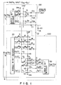
- Fig. 1 shows a D/A converter according to one embodiment of this invention.
- D/A conversion for upper L bits of digital input (DSL to DU1) is effected by segment type capacitor array (Co1 to Cox), and D/A conversion for middle and lower (M+N) bits is effected by substantially two resistor segment type D/A converter sections.
- the digital input is constructed to include three portions: upper L bits (DSL to DS1), middle M bits (DTM to DT1), and lower (DUN to DU1). Data of the upper, middle, and lower bits are respectively decoded by decoders 10, 20, and 30. Decoders 10, 20, and 30 respectively perform decoding operations of those shown in truth tables of tables 1, 2, and 3.
- capacitors Co1 to Cox has the same capacitance (C).
- switches included in switches S1 to Sx and corresponding in number to the contents of L-bit digital signals DSL to DS1, are connected to reference potential terminal Vref.
- output voltage Vout is increased by Vref/2 L each time the content of upper L-bit digital signals DSL to DS1 is increased by "1".
- first resistors R and 2 N second resistors r are serially connected between reference potential terminal Vref and ground potential terminal Vss.
- switches T(2 M -1) to T1 are connected at one end to serial connection nodes N(2 M -1) to N3 of first resistors R, connection node N2 between first resistor R and second resistor r, and connection node N1 between second resistor r and reference potential terminal Vss.
- Switches T(2 M -1) to T1 are commonly connected at the other end P to one electrode of capacitor C1.
- Capacitor C1 has the same capacitance (C) as capacitors Co1 to Cox and is connected at the other electrode to output potential terminal Vout.
- the switching states of 2 M switches T are controlled according to the result OT(2 M -1) to OT(1) of decoding for middle M-bit digital signals DTM to DT1, and one of switches T is selectively turned on according to the content of M-bit digital signal OT.
- the potential at that node (for example, N3) connected to one end of turned-on switch T (for example, T3), or the middle M-bit D/A conversion output, is capacitively coupled to the output of capacitor array type upper L-bit D/A converter section 100, via capacitor C1.
- the middle M-bit D/A conversion output causes the value of output potential Vout to be increased by Vref/2 (L+M) [... (2)] each time the content of M-bit digital signal OT is increased by "1".
- switches U(2 N -1) to U1 are connected at one end to serial connection nodes n(2 N -1) to n2 of second resistors r, and connection node N1 between second resistor r and ground potential terminal Vss.
- Switches U(2 N -1) to U1 are commonly connected at the other end Q to one electrode of capacitor C2 which has the same capacitance as capacitor C1 and which is connected at the other electrode to output potential terminal Vout.
- the switching states of 2 N switches U are controlled according to the result OU(2 N -1) to OU(1) of decoding lower N-bit digital signals DUN to DU1, and one of switches U is selectively turned on according to the content of N-bit digital signal.
- the potential at that node (for example, n2) connected to one end of turn-on switch U (for example, U2), or the lower N-bit D/A conversion output, is capacitively coupled via capacitor C2 to the output of capacitor array type upper L-bit D/A converter section 100 to which the middle M-bit D/A conversion output is capacitively coupled.
- the lower N-bit D/A conversion output causes the value of output potential Vout to be increased by Vref/2 (L+M+N) each time the content of the N-bit digital signal is increased by "1".
- the switching states of switches S, T, and U are, for example, shown as follows: where 1 ⁇ i ⁇ 2 L -1, 1 ⁇ j ⁇ 2 M -1, and 1 ⁇ k ⁇ 2 N -1.
- the D/A converter of Fig. 1 practically uses two D/A converter sections (20+R, 30+r) to effect D/A conversion for the middle and lower (M+N) bits, and produces an output, obtained by capacitively coupling the respective D/A conversion outputs to the upper L-bit D/A conversion output, via capacitors C1 and C2.
- total capacitor area Cs required for the D/A converter is obtained as follows:
- switches S1 to Sx can be directly turned on or off by upper L bits DSL to DS1 without using decoder 10.
- capacitor C0 is shown in Fig. 1 by broken lines and connected at the other electrode to predetermined potential supply terminal Vs. With this connection, the level of output potential Vout can be precisely set by a ratio between the capacitances of capacitors C1 and C0.
- Fig. 2 shows a second embodiment of this invention.
- the D/A converter of Fig. 2 is similar to that of Fig. 1 in that the upper L bits of a digital input (DSL to DS1) are D/A converted by means of (2 N -1) segment type capacitor arrays (Co1 to Cox), and the middle and lower (M+N) bits are D/A converted by means of substantially two D/A converter sections.
- the value of capacitive coupling capacitor C2 is weighted, instead of effecting the weighting by resistors r.
- switches U(2 N -1) to U1 are connected at one end to serial connection nodes N(2 M -2) to N2 of resistors R and connection node N1 between resistor R and ground potential terminal Vss, in the same manner as switches T(2 M -2) to T1, and commonly connected at the other end to one electrode of capacitor C2 whose capacitance is weighted to C1/2 N .
- the middle M-bit D/A conversion output causes the value of output potential Vout to be increased by Vref/2 (L+M) each time the content of M-bit digital signals DTM to DT1 is increased by "1".
- the lower N-bit D/A conversion output causes output potential Vout to be increased by Vref/2 (L+M+N) due to the capacitive coupling by capacitor C2 each time the content of N-bit digital signals DUN to DU1 is increased by "1".
- resistor R can be commonly used for switches T and U, it is possible to make the number of resistors, required for D/A converting the middle and lower (M+N) bits, smaller than that in the D/A converter of Fig. 1.
- resistors R and r may be replaced by diodes or LEDs which are biased in the forward direction. That is, elements R and r are not limited to resistors if desired stable voltages can be derived from connection nodes (N1, N2, N3 ...) between elements R and r.
- a digital signal of a large number of bits can be effectively converted to an analog signal by use of a small number of elements. Further, a monotonic or linear increasing characteristic of a D/A conversion output can be further improved by using segment type capacitor arrays to construct the upper bit D/A converting section.
Landscapes
- Engineering & Computer Science (AREA)
- Theoretical Computer Science (AREA)
- Analogue/Digital Conversion (AREA)
Claims (7)
- Digital-Analog-Wandler, welcher folgendes umfaßt: eine Gruppe von Widerständen (R+r;R), welche zwischen einem Versorgungsspannungspotentialanschluß (Vss) und einem Referenzpotentialanschluß (Vref) in Reihe geschaltet sind;
eine erste Gruppe von Schaltern (T), welche zwischen einem ersten Schaltungspunkt (P) und entsprechenden vorgegebenen seriellen Anschlußknoten (N) der Widerstandsgruppe (R) eingeschaltet und so gesteuert sind, daß einer von ihnen selektiv eingeschaltet wird;
eine zweite Gruppe von Schaltern (U), welche zwischen einem zweiten Schaltungspunkt (Q) und entsprechenden vorgegebenen seriellen Anschlußknoten (n) der Widerstandsgruppe (r) eingeschaltet und so gesteuert sind, daß einer von ihnen selektiv eingeschaltet wird; und
erste und zweite Kondendatoren (C1 und C2), welche zwischen einem Ausgangsanschluß (Vout) und dem ersten Schaltungspunkt (P) bzw. zwischen dem Ausgangsanschluß (Vout) und dem zweiten Schaltungspunkt (Q) eingeschaltet sind,
dadurch gekennzeichnet, daß
die erste Schaltergruppe (T) so gesteuert ist, daß einer von ihnen selektiv entsprechend mittleren Bits (DTM bis DT1) eines digitalen Signals (DSL bis DU1) eingeschaltet wird; und
die zweite Schaltergruppe (U) so gesteuert ist, daß einer von ihnen selektiv entsprechend unteren Bits (DUN bis DU1) des digitalen Signals (DSL bis DU1) eingeschaltet wird. - Digital-Analog-Wandler gemäß Anspruch 1, dadurch gekennzeichnet, daß die Widerstandsgruppe (R+r) eine erste Gruppe in Reihe geschalteter Widerstände (R), von denen jeder einen ersten Widerstandswert hat, sowie eine zweite Gruppe in Reihe geschalteter Widerstände (r), von denen jeder einen zweiten Widerstandswert hat, enthält, wobei die erste und zweite Widerstandsgruppe miteinander in Reihe geschaltet sind und die Gesamtsumme der zweiten Widerstandsgruppe gleich dem ersten Widerstandswert eingestellt ist (R=Σr);
die Schalter der ersten Schaltergruppe (T) zwischen jeweils entsprechenden seriellen Verbindungsknoten (N(2M-1) bis N3) der Widerstände der ersten Widerstandsgruppe (R) bzw. dem ersten Schaltungspunkt (P) eingeschaltet sind;
die Schalter der zweiten Schaltergruppe (U) zwischen jeweils entsprechenden seriellen Verbindungsknoten (n(2N-1) bis n2) der Widerstände der zweiten Widerstandsgruppe (r) bzw. dem zweiten Schaltungspunkt (Q) eingeschaltet sind; und
die Kapazität des ersten Kondensators (C1) im wesentlichen gleich ist (C1=C2) derjenigen des zweiten Kondensators (C2). - Digital-Analog-Wandler gemäß Anspruch 1, dadurch gekennzeichnet, daß die Widerstandsgruppe (R) aus einer Reihe von Widerständen mit im wesentlichen demselben Widerstandswert gebildet ist;
die Schalter der ersten Schaltergruppe (T) zwischen jeweils entsprechenden seriellen Verbindungsknoten (N(2M-1) bis N2) der Widerstände der ersten Widerstandsgruppe (R) bzw. dem ersten Schaltungspunkt (P) eingeschaltet sind;
die Schalter der Schaltergruppe (U) zwischen jeweils entsprechenden seriellen Verbindungsknoten (n(2N-1) bis n2) der Widerstände der zweiten Widerstandsgruppe (r) bzw. dem zweiten Schaltungspunkt (Q) eingeschaltet sind; und
die Kapazität des zweiten Kondensators (C2) im wesentlichen gleich ist dem Wert (C2=C1/2N), welchen man durch Dividieren der Kapazität des ersten Kondensators (C1) durch die Anzahl (2N) der die zweite Schaltergruppe (U) bildenden Schalter erhält. - Digital-Analog-Wandler gemäß einem der Ansprüche 1 bis 3, dadurch gekennzeichnet, daß
die Schalter der ersten Schaltergruppe (T) so gesteuert sind, daß einer von ihnen selektiv entsprechend dem Ergebnis (OT(2M-1) bis OT(1)) der Decodierung der mittleren Bits (DTM bis DT1) eines digitalen Signals (DSL bis DU1) eingeschaltet wird;
die Schalter der zweiten Schaltergruppe (U) so gesteuert sind, daß einer von ihnen selektiv entsprechend dem Ergebnis (OU(2N-1) bis OU(2)) der Decodierung der unteren Bits (DUN bis DU1) des digitalen Signals (DSL bis DU1) eingeschaltet wird;
eine dritte Gruppe von Schaltern (S) vorgesehen ist, von denen ein Ende so gesteuert ist, daß es selektiv mit dem Versorgungsspannungspotentialanschluß (Vss) oder dem Referenzpotentialanschluß (Vref) entsprechend dem Ergebnis (OS(21-1) bis OS(1)) der- Decodierung der oberen Bits (DSL bis DS1) des digitalen Signals (DSL bis DU1) gekoppelt wird; und
eine Gruppe von Kondensatoren (Co1 bis Cox) jeweils zwischen den anderen Enden der Schalter der dritten Schaltergruppe (S) und dem Ausgangsanschluß (Vout) eingeschaltet ist. - Digital-Analog-Wandler gemäß Anspruch 4, dadurch gekennzeichnet, daß
die Kapazitäten der ersten und zweiten Kondensatoren (C1 und C2) im wesentlichen gleich sind (C1=C2=Co1) der Kapazität des einen Kondensators der Kondensatorgruppe (Co1 bis Cox). - Digital-Analog-Wandler gemäß Anspruch 4 oder 5, dadurch gekennzeichnet, daß
die Kapazität des ersten Kondensators (C1) im wesentlichen gleich ist (C1=Co) der Kapazität des Kondensators der Kondensatorgruppe (Co1 bis Cox) und die Kapazität des zweiten Kondensators (C2) im wesentlichen gleich ist dem Wert (C2=C1/2N), welchen man durch Dividieren der Kapazität des ersten Kondensators (C1) durch die Anzahl (2N) der die zweite Schaltergruppe (U) bildenden Schalter erhält. - Digital-Analog-Wandler gemäß Anspruch 4, 5 oder 6, welcher des weiteren einen Ausgangskondensator (Co) umfaßt, der zwischen einer gegebenen festen Potentialschaltung (Vs) und dem Ausgangsanschluß (Vout) eingeschaltet ist.
Applications Claiming Priority (2)
| Application Number | Priority Date | Filing Date | Title |
|---|---|---|---|
| JP62058128A JPS63224415A (ja) | 1987-03-13 | 1987-03-13 | デイジタル−アナログ変換器 |
| JP58128/87 | 1987-03-13 |
Publications (3)
| Publication Number | Publication Date |
|---|---|
| EP0282034A2 EP0282034A2 (de) | 1988-09-14 |
| EP0282034A3 EP0282034A3 (de) | 1991-12-04 |
| EP0282034B1 true EP0282034B1 (de) | 1995-01-25 |
Family
ID=13075344
Family Applications (1)
| Application Number | Title | Priority Date | Filing Date |
|---|---|---|---|
| EP88103722A Expired - Lifetime EP0282034B1 (de) | 1987-03-13 | 1988-03-09 | D/A-Wandler |
Country Status (5)
| Country | Link |
|---|---|
| US (1) | US4873525A (de) |
| EP (1) | EP0282034B1 (de) |
| JP (1) | JPS63224415A (de) |
| KR (1) | KR900008822B1 (de) |
| DE (1) | DE3852832T2 (de) |
Families Citing this family (19)
| Publication number | Priority date | Publication date | Assignee | Title |
|---|---|---|---|---|
| JPH04329025A (ja) * | 1991-04-30 | 1992-11-17 | Toshiba Corp | D/aコンバータ |
| US5283580A (en) * | 1992-09-28 | 1994-02-01 | Motorola, Inc. | Current/resistor digital-to-analog converter having enhanced integral linearity and method of operation |
| US5332997A (en) * | 1992-11-04 | 1994-07-26 | Rca Thomson Licensing Corporation | Switched capacitor D/A converter |
| JPH088465B2 (ja) * | 1992-11-20 | 1996-01-29 | 日本電気株式会社 | スイッチトキャパシタ回路 |
| JPH0760301B2 (ja) * | 1992-12-02 | 1995-06-28 | 日本電気株式会社 | 液晶駆動回路 |
| US5396245A (en) * | 1993-01-21 | 1995-03-07 | Linear Technology Corporation | Digital to analog converter |
| US5469164A (en) * | 1993-09-30 | 1995-11-21 | Ford Motor Company | Circuit and method for digital to analog signal conversion |
| USRE38083E1 (en) | 1994-03-18 | 2003-04-22 | Analog Devices, Inc. | Rail-to-rail DAC drive circuit |
| US5471208A (en) * | 1994-05-20 | 1995-11-28 | David Sarnoff Research Center, Inc. | Reference ladder auto-calibration circuit for an analog to digital converter |
| US5781139A (en) * | 1996-03-19 | 1998-07-14 | Thomson Multimedia S.A. | Switched capacitor digital-to analog converter |
| US5760726A (en) * | 1996-08-23 | 1998-06-02 | Motorola, Inc. | Digital-to-analog converter with dynamic matching and bit splitting |
| US6225929B1 (en) | 1998-12-02 | 2001-05-01 | Hewlett-Packard Company | Digital-to-analog converter having switchable current sources and resistor string |
| US6297759B1 (en) * | 2000-05-25 | 2001-10-02 | Lewyn Consulting, Inc. | Digital-to-analog converter with high-speed output |
| US6937178B1 (en) | 2003-05-15 | 2005-08-30 | Linear Technology Corporation | Gradient insensitive split-core digital to analog converter |
| EP1770867B1 (de) * | 2005-09-08 | 2017-05-31 | Marvell World Trade Ltd. | Kapazitiver Digital Analog Wandler und Analog Digital Wandler |
| US7439896B2 (en) | 2005-09-08 | 2008-10-21 | Marvell World Trade Ltd. | Capacitive digital to analog and analog to digital converters |
| TWI332325B (en) * | 2005-11-05 | 2010-10-21 | Samsung Electronics Co Ltd | Digital/analog converting driver and method |
| US8242944B2 (en) | 2007-04-26 | 2012-08-14 | Renesas Electronics Corporation | Digital-to-analog converter circuit including adder drive circuit and display |
| JP6421537B2 (ja) * | 2014-10-15 | 2018-11-14 | セイコーエプソン株式会社 | ドライバー及び電子機器 |
Family Cites Families (9)
| Publication number | Priority date | Publication date | Assignee | Title |
|---|---|---|---|---|
| US3997892A (en) * | 1973-07-27 | 1976-12-14 | Trw Inc. | Digital to analog converter with improved companding |
| US4200863A (en) * | 1977-10-03 | 1980-04-29 | The Regents Of The University Of California | Weighted capacitor analog/digital converting apparatus and method |
| US4198622A (en) * | 1978-02-21 | 1980-04-15 | National Semiconductor Corporation | Double digital-to-analog converter |
| US4384277A (en) * | 1981-05-08 | 1983-05-17 | Motorola, Inc. | Digital to analog converter |
| JPS57202126A (en) * | 1981-06-05 | 1982-12-10 | Toko Inc | Digital-to-analog converter |
| JPS59161916A (ja) * | 1983-03-07 | 1984-09-12 | Nec Corp | アナログ−デイジタル変換器 |
| JPS59163912A (ja) * | 1983-03-08 | 1984-09-17 | Toshiba Corp | C−r型da変換器 |
| JPH0652872B2 (ja) * | 1983-12-21 | 1994-07-06 | 沖電気工業株式会社 | ディジタルアナログ変換器 |
| DE3533887C2 (de) * | 1985-09-23 | 1994-07-28 | Siemens Ag | Schaltungsanordnung zur Digital-Analog-Wandlung digitaler Informationen |
-
1987
- 1987-03-13 JP JP62058128A patent/JPS63224415A/ja active Pending
-
1988
- 1988-03-08 US US07/165,702 patent/US4873525A/en not_active Expired - Lifetime
- 1988-03-09 EP EP88103722A patent/EP0282034B1/de not_active Expired - Lifetime
- 1988-03-09 DE DE3852832T patent/DE3852832T2/de not_active Expired - Fee Related
- 1988-03-11 KR KR1019880002528A patent/KR900008822B1/ko not_active Expired
Also Published As
| Publication number | Publication date |
|---|---|
| JPS63224415A (ja) | 1988-09-19 |
| KR900008822B1 (ko) | 1990-11-30 |
| US4873525A (en) | 1989-10-10 |
| EP0282034A3 (de) | 1991-12-04 |
| DE3852832T2 (de) | 1995-05-18 |
| EP0282034A2 (de) | 1988-09-14 |
| KR880012021A (ko) | 1988-10-31 |
| DE3852832D1 (de) | 1995-03-09 |
Similar Documents
| Publication | Publication Date | Title |
|---|---|---|
| US4873525A (en) | Compact R segment D/A converter | |
| US4638303A (en) | Digital-analog converter | |
| US6268817B1 (en) | Digital-to-analog converter | |
| US5426431A (en) | Analog/digital converter | |
| US7501970B2 (en) | Digital to analog converter architecture and method having low switch count and small output impedance | |
| US20030197636A1 (en) | High resolution, high speed, low power switched capacitor analog to digital converter | |
| EP0153778A2 (de) | Mehrschritt-Parallelanalog/Digitalwandler | |
| US5434569A (en) | Methods for adjusting the coupling capacitor of a multi-stage weighted capacitor A/D converter | |
| US9887703B1 (en) | Area efficient digital to analog and analog to digital converters | |
| US6225931B1 (en) | D/A converter with a gamma correction circuit | |
| US4611195A (en) | Digital-to-analog converter | |
| KR100814255B1 (ko) | 디지털-아날로그 변환기 | |
| US6400298B1 (en) | Digital-to-analog converter with fast switching and precise voltage conversion | |
| US7259706B2 (en) | Balanced dual resistor string digital to analog converter system and method | |
| EP0681372B1 (de) | Schaltung zur Digital-/Analogumsetzung und die Schaltung benutzender A/D-Wandler | |
| JP2837726B2 (ja) | ディジタル・アナログ変換器 | |
| US20060261991A1 (en) | Digital-to-analog converter | |
| US7295142B2 (en) | Digital-to-analog converter with short integration time constant | |
| JP2737927B2 (ja) | 抵抗分圧型ディジタル−アナログ変換器 | |
| JP2001127634A (ja) | ディジタル・アナログ変換器 | |
| EP0247065B1 (de) | Ungetrimmter 12-bit monotonischer all-kapazitiver a-d-wandler | |
| JPH11340830A (ja) | 逐次比較型a/dコンバータ回路 | |
| CN111933073B (zh) | 一种灰阶电压产生电路 | |
| US6639536B2 (en) | Digital-analog converter | |
| JP2919148B2 (ja) | A/d変換器 |
Legal Events
| Date | Code | Title | Description |
|---|---|---|---|
| PUAI | Public reference made under article 153(3) epc to a published international application that has entered the european phase |
Free format text: ORIGINAL CODE: 0009012 |
|
| 17P | Request for examination filed |
Effective date: 19880406 |
|
| AK | Designated contracting states |
Kind code of ref document: A2 Designated state(s): DE FR GB |
|
| PUAL | Search report despatched |
Free format text: ORIGINAL CODE: 0009013 |
|
| AK | Designated contracting states |
Kind code of ref document: A3 Designated state(s): DE FR GB |
|
| 17Q | First examination report despatched |
Effective date: 19931129 |
|
| GRAA | (expected) grant |
Free format text: ORIGINAL CODE: 0009210 |
|
| AK | Designated contracting states |
Kind code of ref document: B1 Designated state(s): DE FR GB |
|
| REF | Corresponds to: |
Ref document number: 3852832 Country of ref document: DE Date of ref document: 19950309 |
|
| ET | Fr: translation filed | ||
| PLBE | No opposition filed within time limit |
Free format text: ORIGINAL CODE: 0009261 |
|
| STAA | Information on the status of an ep patent application or granted ep patent |
Free format text: STATUS: NO OPPOSITION FILED WITHIN TIME LIMIT |
|
| 26N | No opposition filed | ||
| PGFP | Annual fee paid to national office [announced via postgrant information from national office to epo] |
Ref country code: GB Payment date: 19980302 Year of fee payment: 11 |
|
| PGFP | Annual fee paid to national office [announced via postgrant information from national office to epo] |
Ref country code: DE Payment date: 19980313 Year of fee payment: 11 |
|
| PG25 | Lapsed in a contracting state [announced via postgrant information from national office to epo] |
Ref country code: GB Free format text: LAPSE BECAUSE OF NON-PAYMENT OF DUE FEES Effective date: 19990309 |
|
| REG | Reference to a national code |
Ref country code: FR Ref legal event code: D6 |
|
| GBPC | Gb: european patent ceased through non-payment of renewal fee |
Effective date: 19990309 |
|
| PG25 | Lapsed in a contracting state [announced via postgrant information from national office to epo] |
Ref country code: DE Free format text: LAPSE BECAUSE OF NON-PAYMENT OF DUE FEES Effective date: 20000101 |
|
| PGFP | Annual fee paid to national office [announced via postgrant information from national office to epo] |
Ref country code: FR Payment date: 20070308 Year of fee payment: 20 |