EP0282407A2 - Dispositif semi-conducteur utilisant des puits quantiques multiples - Google Patents
Dispositif semi-conducteur utilisant des puits quantiques multiples Download PDFInfo
- Publication number
- EP0282407A2 EP0282407A2 EP88400541A EP88400541A EP0282407A2 EP 0282407 A2 EP0282407 A2 EP 0282407A2 EP 88400541 A EP88400541 A EP 88400541A EP 88400541 A EP88400541 A EP 88400541A EP 0282407 A2 EP0282407 A2 EP 0282407A2
- Authority
- EP
- European Patent Office
- Prior art keywords
- layer
- semiconductor device
- quantum well
- barrier
- layers
- Prior art date
- Legal status (The legal status is an assumption and is not a legal conclusion. Google has not performed a legal analysis and makes no representation as to the accuracy of the status listed.)
- Ceased
Links
Images



Classifications
-
- H—ELECTRICITY
- H10—SEMICONDUCTOR DEVICES; ELECTRIC SOLID-STATE DEVICES NOT OTHERWISE PROVIDED FOR
- H10H—INORGANIC LIGHT-EMITTING SEMICONDUCTOR DEVICES HAVING POTENTIAL BARRIERS
- H10H20/00—Individual inorganic light-emitting semiconductor devices having potential barriers, e.g. light-emitting diodes [LED]
- H10H20/80—Constructional details
- H10H20/81—Bodies
- H10H20/811—Bodies having quantum effect structures or superlattices, e.g. tunnel junctions
- H10H20/812—Bodies having quantum effect structures or superlattices, e.g. tunnel junctions within the light-emitting regions, e.g. having quantum confinement structures
-
- B—PERFORMING OPERATIONS; TRANSPORTING
- B82—NANOTECHNOLOGY
- B82Y—SPECIFIC USES OR APPLICATIONS OF NANOSTRUCTURES; MEASUREMENT OR ANALYSIS OF NANOSTRUCTURES; MANUFACTURE OR TREATMENT OF NANOSTRUCTURES
- B82Y20/00—Nanooptics, e.g. quantum optics or photonic crystals
-
- H—ELECTRICITY
- H01—ELECTRIC ELEMENTS
- H01S—DEVICES USING THE PROCESS OF LIGHT AMPLIFICATION BY STIMULATED EMISSION OF RADIATION [LASER] TO AMPLIFY OR GENERATE LIGHT; DEVICES USING STIMULATED EMISSION OF ELECTROMAGNETIC RADIATION IN WAVE RANGES OTHER THAN OPTICAL
- H01S5/00—Semiconductor lasers
- H01S5/04—Processes or apparatus for excitation, e.g. pumping, e.g. by electron beams
- H01S5/042—Electrical excitation ; Circuits therefor
- H01S5/0421—Electrical excitation ; Circuits therefor characterised by the semiconducting contacting layers
- H01S5/0422—Electrical excitation ; Circuits therefor characterised by the semiconducting contacting layers with n- and p-contacts on the same side of the active layer
-
- H—ELECTRICITY
- H01—ELECTRIC ELEMENTS
- H01S—DEVICES USING THE PROCESS OF LIGHT AMPLIFICATION BY STIMULATED EMISSION OF RADIATION [LASER] TO AMPLIFY OR GENERATE LIGHT; DEVICES USING STIMULATED EMISSION OF ELECTROMAGNETIC RADIATION IN WAVE RANGES OTHER THAN OPTICAL
- H01S5/00—Semiconductor lasers
- H01S5/30—Structure or shape of the active region; Materials used for the active region
- H01S5/34—Structure or shape of the active region; Materials used for the active region comprising quantum well or superlattice structures, e.g. single quantum well [SQW] lasers, multiple quantum well [MQW] lasers or graded index separate confinement heterostructure [GRINSCH] lasers
-
- H—ELECTRICITY
- H10—SEMICONDUCTOR DEVICES; ELECTRIC SOLID-STATE DEVICES NOT OTHERWISE PROVIDED FOR
- H10D—INORGANIC ELECTRIC SEMICONDUCTOR DEVICES
- H10D48/00—Individual devices not covered by groups H10D1/00 - H10D44/00
- H10D48/30—Devices controlled by electric currents or voltages
- H10D48/32—Devices controlled by only the electric current supplied, or only the electric potential applied, to an electrode which does not carry the current to be rectified, amplified or switched
- H10D48/36—Unipolar devices
- H10D48/362—Unipolar transistors having ohmic electrodes on emitter-like, base-like, and collector-like regions, e.g. hot electron transistors [HET], metal base transistors [MBT], resonant tunnelling transistors [RTT], bulk barrier transistors [BBT], planar doped barrier transistors [PDBT] or charge injection transistors [CHINT]
-
- H—ELECTRICITY
- H10—SEMICONDUCTOR DEVICES; ELECTRIC SOLID-STATE DEVICES NOT OTHERWISE PROVIDED FOR
- H10D—INORGANIC ELECTRIC SEMICONDUCTOR DEVICES
- H10D62/00—Semiconductor bodies, or regions thereof, of devices having potential barriers
- H10D62/80—Semiconductor bodies, or regions thereof, of devices having potential barriers characterised by the materials
- H10D62/81—Semiconductor bodies, or regions thereof, of devices having potential barriers characterised by the materials of structures exhibiting quantum-confinement effects, e.g. single quantum wells; of structures having periodic or quasi-periodic potential variation
- H10D62/815—Semiconductor bodies, or regions thereof, of devices having potential barriers characterised by the materials of structures exhibiting quantum-confinement effects, e.g. single quantum wells; of structures having periodic or quasi-periodic potential variation of structures having periodic or quasi-periodic potential variation, e.g. superlattices or multiple quantum wells [MQW]
- H10D62/8161—Semiconductor bodies, or regions thereof, of devices having potential barriers characterised by the materials of structures exhibiting quantum-confinement effects, e.g. single quantum wells; of structures having periodic or quasi-periodic potential variation of structures having periodic or quasi-periodic potential variation, e.g. superlattices or multiple quantum wells [MQW] potential variation due to variations in composition or crystallinity, e.g. heterojunction superlattices
- H10D62/8162—Semiconductor bodies, or regions thereof, of devices having potential barriers characterised by the materials of structures exhibiting quantum-confinement effects, e.g. single quantum wells; of structures having periodic or quasi-periodic potential variation of structures having periodic or quasi-periodic potential variation, e.g. superlattices or multiple quantum wells [MQW] potential variation due to variations in composition or crystallinity, e.g. heterojunction superlattices having quantum effects only in the vertical direction, i.e. layered structures having quantum effects solely resulting from vertical potential variation
- H10D62/8164—Semiconductor bodies, or regions thereof, of devices having potential barriers characterised by the materials of structures exhibiting quantum-confinement effects, e.g. single quantum wells; of structures having periodic or quasi-periodic potential variation of structures having periodic or quasi-periodic potential variation, e.g. superlattices or multiple quantum wells [MQW] potential variation due to variations in composition or crystallinity, e.g. heterojunction superlattices having quantum effects only in the vertical direction, i.e. layered structures having quantum effects solely resulting from vertical potential variation comprising only semiconductor materials
-
- H—ELECTRICITY
- H10—SEMICONDUCTOR DEVICES; ELECTRIC SOLID-STATE DEVICES NOT OTHERWISE PROVIDED FOR
- H10D—INORGANIC ELECTRIC SEMICONDUCTOR DEVICES
- H10D8/00—Diodes
- H10D8/70—Tunnel-effect diodes
- H10D8/755—Resonant tunneling diodes [RTD]
-
- H—ELECTRICITY
- H10—SEMICONDUCTOR DEVICES; ELECTRIC SOLID-STATE DEVICES NOT OTHERWISE PROVIDED FOR
- H10F—INORGANIC SEMICONDUCTOR DEVICES SENSITIVE TO INFRARED RADIATION, LIGHT, ELECTROMAGNETIC RADIATION OF SHORTER WAVELENGTH OR CORPUSCULAR RADIATION
- H10F77/00—Constructional details of devices covered by this subclass
- H10F77/10—Semiconductor bodies
- H10F77/14—Shape of semiconductor bodies; Shapes, relative sizes or dispositions of semiconductor regions within semiconductor bodies
- H10F77/146—Superlattices; Multiple quantum well structures
-
- H—ELECTRICITY
- H01—ELECTRIC ELEMENTS
- H01S—DEVICES USING THE PROCESS OF LIGHT AMPLIFICATION BY STIMULATED EMISSION OF RADIATION [LASER] TO AMPLIFY OR GENERATE LIGHT; DEVICES USING STIMULATED EMISSION OF ELECTROMAGNETIC RADIATION IN WAVE RANGES OTHER THAN OPTICAL
- H01S5/00—Semiconductor lasers
- H01S5/30—Structure or shape of the active region; Materials used for the active region
- H01S5/34—Structure or shape of the active region; Materials used for the active region comprising quantum well or superlattice structures, e.g. single quantum well [SQW] lasers, multiple quantum well [MQW] lasers or graded index separate confinement heterostructure [GRINSCH] lasers
- H01S5/3408—Structure or shape of the active region; Materials used for the active region comprising quantum well or superlattice structures, e.g. single quantum well [SQW] lasers, multiple quantum well [MQW] lasers or graded index separate confinement heterostructure [GRINSCH] lasers characterised by specially shaped wells, e.g. triangular
-
- H—ELECTRICITY
- H01—ELECTRIC ELEMENTS
- H01S—DEVICES USING THE PROCESS OF LIGHT AMPLIFICATION BY STIMULATED EMISSION OF RADIATION [LASER] TO AMPLIFY OR GENERATE LIGHT; DEVICES USING STIMULATED EMISSION OF ELECTROMAGNETIC RADIATION IN WAVE RANGES OTHER THAN OPTICAL
- H01S5/00—Semiconductor lasers
- H01S5/30—Structure or shape of the active region; Materials used for the active region
- H01S5/34—Structure or shape of the active region; Materials used for the active region comprising quantum well or superlattice structures, e.g. single quantum well [SQW] lasers, multiple quantum well [MQW] lasers or graded index separate confinement heterostructure [GRINSCH] lasers
- H01S5/3418—Structure or shape of the active region; Materials used for the active region comprising quantum well or superlattice structures, e.g. single quantum well [SQW] lasers, multiple quantum well [MQW] lasers or graded index separate confinement heterostructure [GRINSCH] lasers using transitions from higher quantum levels
-
- H—ELECTRICITY
- H01—ELECTRIC ELEMENTS
- H01S—DEVICES USING THE PROCESS OF LIGHT AMPLIFICATION BY STIMULATED EMISSION OF RADIATION [LASER] TO AMPLIFY OR GENERATE LIGHT; DEVICES USING STIMULATED EMISSION OF ELECTROMAGNETIC RADIATION IN WAVE RANGES OTHER THAN OPTICAL
- H01S5/00—Semiconductor lasers
- H01S5/30—Structure or shape of the active region; Materials used for the active region
- H01S5/34—Structure or shape of the active region; Materials used for the active region comprising quantum well or superlattice structures, e.g. single quantum well [SQW] lasers, multiple quantum well [MQW] lasers or graded index separate confinement heterostructure [GRINSCH] lasers
- H01S5/3425—Structure or shape of the active region; Materials used for the active region comprising quantum well or superlattice structures, e.g. single quantum well [SQW] lasers, multiple quantum well [MQW] lasers or graded index separate confinement heterostructure [GRINSCH] lasers comprising couples wells or superlattices
Definitions
- the present invention generally relates to semiconductor devices, and more particularly to a semiconductor device utilizing multiquantum wells.
- a quantum well refers to a square potential well having a potential of such a size that electrons or holes confined therein show a quantum effect, and quantum states of different energies (levels) are generated within the quantum well.
- carriers may with a certain rate (probability) move by tunneling between the quantum wells.
- the tunneling rate of the carriers at a certain quantum level in a first quantum well becomes large when a second quantum well has a quantum level identical to or close to that of the first quantum well, and becomes small when the second quantum well does not have a quantum level close to that of the first quantum well.
- the conventional semiconductor element such as the negative resistance element either uses no quantum well or simply uses a single quantum well. For this reason, the negative resistance element suffers the following deficiencies.
- the Esaki diode having a p+-n+ junction, which is a kind of negative resistance element, it is necessary to heavily dope the p+-type and n+-type regions of the Esaki diode.
- the Esaki diode should be operated below a certain temperature such that the effects of impurity diffusion and drift can be neglected.
- a resonant tunnel diode which uses a single quantum well, that is, double potential barriers, but a ratio between a peak current at a resonant point and a valley current at a non-resonant point is small, because the valley current is added with a current component of inelastic tunnel.
- the inelastic tunnel refers to the tunnel caused by the inelastic scattering of the carriers.
- the wavelength of the emitted light is limited by the energy band gap
- the light emitting operation is slow because it is dependent on the p-n recombination rate
- the half-width and monochromaticity are poor because a transition takes place among a plurality of different quantum states
- the frequency of the light modulation is governed by the carrier storage time and cannot be increased.
- the photodiode does not operate unless the bias voltage is set to a sufficiently large voltage, and it is difficult to operate the photodiode at a high speed since the operation speed is determined by the transit time of the carriers in a depletion region.
- Another and more specific object of the present invention is to provide a semiconductor device provided with multiquantum wells having a bottom of conduction band with an energy described by a curve of second order. Such wells are the so-called "parabolic wells".
- the semiconductor device of the present invention it is possible to set a logic amplitude to a large value because it is possible to obtain a large ratio between a peak current and a valley current in a negative resistance characteristic of a transistor or tunnel diode.
- a light emitting device such as an active device and a semiconductor laser
- a light receiving device it is possible to obtain a high sensitivity with ease.
- Still another object of the present invention is to provide a semiconductor device comprising a first barrier layer, a quantum well layer formed on the first barrier layer and having a bottom of conduction band with an energy which varies with a curve of second order, a second barrier layer formed on said quantum well layer, and first and second contact layers.
- the first barrier layer, the quantum well layer and the second barrier layer make up a layer sequence which is repeated a predetermined number of times, and the first contact layer connects to the first barrier layer in a first of the predetermined number of layer sequences, while the second contact layer connects to the second barrier layer in a last of the predetermined number of layer sequences.
- the semiconductor device may be a negative resistance diode, a hot electron transistor, a laser diode, a photodetector and the like.
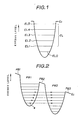
- FIG.1 shows an energy band diagram of this quantum well.
- the electrons will be assumed to be the carriers in the description given hereunder.
- the quantum well having the bottom of conduction band with the energy described by the curve of second order will simply be referred as a quantum well having a potential described by a curve of second order. This kind of quantum well is sometimes called "parabolic well”.
- E C denotes the energy level at the bottom of the conduction band
- EL0 denotes a ground state within the quantum well
- EL1, EL2, ... denote excited states within the quantum well
- EL denotes the excited states within the quantum well as a whole.
- the energy E C that is, the potential of the quantum well, is described a curve of second order which is concave upward.
- E n (n + 1/2) ⁇ , where n is a positive integer including zero, is equal to h/2 ⁇ where h denotes Planck's constant, and ⁇ is equal to (K/m*) 1/2 where K denotes a second derivative of the potential and m* denotes the effective mass.
- the quantum levels exist at equal energy intervals.
- the tunneling rate decreases sharply.
- the reason for this sharp decrease in the tunneling rate is not only due to the fact that the tunneling rate at one potential barrier decreases, but also because a plurality of such potential barriers must be penetrated. Hence, a valley current at a non-resonant point is small.
- the quantum efficiency becomes extremely high, and the electrons move ballistically at a high speed making it possible to modulate the light at a high frequency.
- FIGS.2 and 3 show energy band diagrams for a case where two quantum wells having the potential described by the curve of second order are arranged adjacently and a case where three quantum wells having the potential described by the curve of second order are arranged adjacently, respectively.
- the same designations are used as in FIG.1.
- e denotes the electrons
- PB1 through PB4 denote barrier layers
- PW1 through PW3 denote well layers.
- the quantum levels in the well layers PW1 through PW3 all exist at equal energy intervals, and these quantum levels will always coincide when an appropriate bias voltage is applied across two ends of the quantum well arrangement.
- the electrons e can tunnel through the potential barriers of the barrier layers PB1 through PB4.
- FIG.4 shows an energy band diagram for explaining a case where a transition from the first excited state to the ground state occurs successively in the three quantum wells PW1 through PW3 shown in FIG.3.
- arrows F indicate that the electrons e undergo transition between the excited state and the ground state after the tunneling.
- the semiconductor device according to the present invention uses multiquantum wells having the potential described by the curve of second order.
- FIG.5 shows an embodiment of the semiconductor device according to the present invention.
- FIG.5 shows an essential part of a negative resistance diode, but the construction will be similar for a photodiode.
- the negative resistance diode comprises an n+-type gallium arsenide (GaAs) substrate 1, an aluminum gallium arsenide (Al x Ga 1-x As) buffer layer 2, Al x Ga 1-x As barrier layers 3, well layers 4 each made up of a first layer made of Al x Ga 1-x As, a second layer made of GaAs and a third layer made of Al x Ga 1-x As, an n+-type GaAs electrode contact layer 5, and electrodes 6 and 7.
- the barrier layers 3 and the well layers 4 constitute the quantum well having the potential described by the curve of second order.
- the substrate 1 has an impurity concentration of 1 ⁇ 1018 cm ⁇ 3
- the buffer layer 2 has an Al content x of 0.3 and a film thickness of 2000 ⁇
- the barrier layers 3 have an Al content x of 0.3 and a film thickness of 100 ⁇
- the well layers 4 have a film thickness of 200 ⁇
- the electrode contact layer 5 has an impurity concentration of 2 ⁇ 1018 cm ⁇ 3 and a film thickness of 4000 ⁇
- the electrodes 6 and 7 are made of gold germanium (AuGe) (or gold (Au)) and have a film thickness of 200 ⁇ (or 3000 ⁇ ).
- the first AlGaAs layer of the well layer 4 has an Al content x of 0.3
- the second GaAs layer of the well layer 4 has an Al content x of 0.00
- the third AlGaAs layer of the well layer 4 has an Al content x of 0.3.
- FIG.6 shows another embodiment of the semiconductor device according to the present invention.
- FIG.6 shows an essential part of a semiconductor laser (or laser diode).
- the semiconductor laser comprises an n+-type GaAs substrate 21, an n-type Al x Ga 1-x As cladding layer 22, Al x Ga 1-x As barrier layers 23, well layers 24 each made up of a first layer made of Al x Ga 1-x As, a second layer made of GaAs and a third layer made of Al x Ga 1-x As, an n-type Al x Ga 1-x As cladding layer 25, an n+-type GaAs electrode contact layer 26, an intrinsic Al x Ga 1-x As buried layer 27, a silicon dioxide (SiO2) insulator layer 28, and electrodes 29 and 30.
- the barrier layers 23 and the well layers 24 constitute the quantum well having the potential described by the curve of second order and act as an activation layer.
- the substrate 21 has an impurity concentration of 1 ⁇ 1018 cm ⁇ 3
- the cladding layer 22 has a film thickness of 2000 ⁇
- the barrier layers 23 have a film thickness of 100 ⁇ and an Al content x of 0.3
- the well layers 24 have a film thickness of 200 ⁇
- the cladding layer 25 has a film thickness of 2000 ⁇
- the electrode contact layer 26 has a film thickness of 4000 ⁇ and an impurity concentration of 2 ⁇ 1018 cm ⁇ 3
- the buried layer 27 has a film thickness of 11000 ⁇
- the insulator layer 28 has a film thickness of 4000 ⁇
- the electrodes 29 and 30 are made of AuGe (or Au)
- the first AlGaAs layer of the well layer 24 has an Al content x of 0.3
- the second GaAs layer of the well layer 24 has an Al content x of 0.00
- the third AlGaAs layer of the well layer 24 has an Al content x of 0.3.
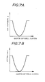
- FIGS.7A and 7B show diagrams for explaining a method of forming the quantum well having the potential described by the curve of second order.
- FIG.7A shows the relationship between the depth of the well layer and the Al content x thereof
- FIG.7B shows the relationship between the depth of the well layer and the potential thereof.
- FIGS.8A and 8B show diagrams for explaining another method of forming the quantum well having the potential described by the curve of second order.
- FIG.8A shows the relationship between the depth of the well layer and the Al content x thereof
- FIG.8B shows the relationship between the depth of the well layer and the potential thereof.
- the quantum well having the potential described by the curve of second order is formed by varying the film thickness of the well layer while maintaining the Al content x and the film thickness of the barrier layer constant.
- the present invention may be applied to semiconductor devices other than those of the embodiments described before. For example, it is possible to improve various characteristics of a hot electron transistor (or resonant hot electron transistor) by inserting the quantum well having the potential described by the curve of second order as a potential barrier between emitter and base of the hot electron transistor. In addition, it is possible to use indium phosphor (InP) or indium aluminum arsenide (InAlAs) in place of AlGaAs, and use indium gallium arsenide (InGaAs) in place of GaAs.
- InP indium phosphor
- InAlAs indium aluminum arsenide
- InGaAs indium gallium arsenide
Landscapes
- Physics & Mathematics (AREA)
- Optics & Photonics (AREA)
- Engineering & Computer Science (AREA)
- Condensed Matter Physics & Semiconductors (AREA)
- General Physics & Mathematics (AREA)
- Electromagnetism (AREA)
- Nanotechnology (AREA)
- Chemical & Material Sciences (AREA)
- Biophysics (AREA)
- Crystallography & Structural Chemistry (AREA)
- Life Sciences & Earth Sciences (AREA)
- Semiconductor Lasers (AREA)
- Bipolar Transistors (AREA)
- Light Receiving Elements (AREA)
- Junction Field-Effect Transistors (AREA)
Applications Claiming Priority (2)
| Application Number | Priority Date | Filing Date | Title |
|---|---|---|---|
| JP53134/87 | 1987-03-10 | ||
| JP62053134A JPH0797688B2 (ja) | 1987-03-10 | 1987-03-10 | 半導体装置 |
Publications (2)
| Publication Number | Publication Date |
|---|---|
| EP0282407A2 true EP0282407A2 (fr) | 1988-09-14 |
| EP0282407A3 EP0282407A3 (fr) | 1989-08-23 |
Family
ID=12934349
Family Applications (1)
| Application Number | Title | Priority Date | Filing Date |
|---|---|---|---|
| EP88400541A Ceased EP0282407A3 (fr) | 1987-03-10 | 1988-03-08 | Dispositif semi-conducteur utilisant des puits quantiques multiples |
Country Status (3)
| Country | Link |
|---|---|
| US (1) | US4868612A (fr) |
| EP (1) | EP0282407A3 (fr) |
| JP (1) | JPH0797688B2 (fr) |
Cited By (2)
| Publication number | Priority date | Publication date | Assignee | Title |
|---|---|---|---|---|
| EP0574947A1 (fr) * | 1992-06-19 | 1993-12-22 | Sony Corporation | Dispositif d'émission de la lumière |
| CN104638028A (zh) * | 2015-02-17 | 2015-05-20 | 天津大学 | 一种具有新型材料结构的矩形微带贴片天线太赫兹波源 |
Families Citing this family (10)
| Publication number | Priority date | Publication date | Assignee | Title |
|---|---|---|---|---|
| US5045894A (en) * | 1988-06-29 | 1991-09-03 | Hitachi, Ltd. | Compound semiconductor light emitting device |
| US4963714A (en) * | 1988-10-24 | 1990-10-16 | Raytheon Company | Diode laser soldering system |
| JPH03241875A (ja) * | 1990-02-20 | 1991-10-29 | Nippon Telegr & Teleph Corp <Ntt> | 半導体共鳴トンネルダイオード |
| US5362977A (en) * | 1992-12-28 | 1994-11-08 | At&T Bell Laboratories | Single mirror light-emitting diodes with enhanced intensity |
| US5488234A (en) * | 1993-03-18 | 1996-01-30 | Matsushita Electric Industrial Co., Ltd. | Semiconductor element having bivalent and VI group element and an insulating layer |
| US5552603A (en) * | 1994-09-15 | 1996-09-03 | Martin Marietta Corporation | Bias and readout for multicolor quantum well detectors |
| US6664605B1 (en) * | 2000-03-31 | 2003-12-16 | Triquint Technology Holding Co. | Dopant diffusion blocking for optoelectronic devices using InAlAs and/or InGaAlAs |
| US6490193B1 (en) * | 2001-08-22 | 2002-12-03 | Raytheon Company | Forming and storing data in a memory cell |
| US8124959B2 (en) * | 2007-06-28 | 2012-02-28 | Intel Corporation | High hole mobility semiconductor device |
| US8541773B2 (en) * | 2011-05-02 | 2013-09-24 | Intel Corporation | Vertical tunneling negative differential resistance devices |
Family Cites Families (6)
| Publication number | Priority date | Publication date | Assignee | Title |
|---|---|---|---|---|
| US4257055A (en) * | 1979-07-26 | 1981-03-17 | University Of Illinois Foundation | Negative resistance heterojunction devices |
| JPS57176785A (en) * | 1981-04-22 | 1982-10-30 | Hitachi Ltd | Semiconductor laser device |
| JPS5990978A (ja) * | 1982-11-16 | 1984-05-25 | Nec Corp | 超格子負性抵抗素子 |
| JPS6158268A (ja) * | 1984-08-30 | 1986-03-25 | Fujitsu Ltd | 高速半導体装置 |
| US4745452A (en) * | 1984-09-24 | 1988-05-17 | Massachusetts Institute Of Technology | Tunneling transfer devices |
| JPS63161690A (ja) * | 1986-12-25 | 1988-07-05 | Nec Corp | 量子井戸型半導体レ−ザ |
-
1987
- 1987-03-10 JP JP62053134A patent/JPH0797688B2/ja not_active Expired - Fee Related
-
1988
- 1988-03-07 US US07/165,050 patent/US4868612A/en not_active Expired - Lifetime
- 1988-03-08 EP EP88400541A patent/EP0282407A3/fr not_active Ceased
Cited By (4)
| Publication number | Priority date | Publication date | Assignee | Title |
|---|---|---|---|---|
| EP0574947A1 (fr) * | 1992-06-19 | 1993-12-22 | Sony Corporation | Dispositif d'émission de la lumière |
| US5471067A (en) * | 1992-06-19 | 1995-11-28 | Sony Corporation | Semiconductor metal contacting structure and a light emitting device |
| CN104638028A (zh) * | 2015-02-17 | 2015-05-20 | 天津大学 | 一种具有新型材料结构的矩形微带贴片天线太赫兹波源 |
| CN104638028B (zh) * | 2015-02-17 | 2017-09-19 | 天津大学 | 一种具有新型材料结构的矩形微带贴片天线太赫兹波源 |
Also Published As
| Publication number | Publication date |
|---|---|
| JPS63220591A (ja) | 1988-09-13 |
| EP0282407A3 (fr) | 1989-08-23 |
| JPH0797688B2 (ja) | 1995-10-18 |
| US4868612A (en) | 1989-09-19 |
Similar Documents
| Publication | Publication Date | Title |
|---|---|---|
| Milnes | Heterojunctions and metal semiconductor junctions | |
| Capasso et al. | Quantum functional devices: resonant-tunneling transistors, circuits with reduced complexity, and multiple valued logic | |
| US4383269A (en) | Graded bandgap photodetector | |
| Döhler et al. | I n situ grown‐in selective contacts to n‐i‐p‐i doping superlattice crystals using molecular beam epitaxial growth through a shadow mask | |
| US4868612A (en) | Semiconductor device utilizing multiquantum wells | |
| US4801993A (en) | Monolithic semiconductor structure of a heterojunction bipolar transistor and a laser | |
| GB2226916A (en) | Optically controlled resonant tunnelling electronic devices | |
| EP0393317A2 (fr) | Dispositifs semi-conducteurs à effet tunnel résonnant | |
| EP0530942B1 (fr) | Dispositif de commutation opto-électronique à puits quantiques à émission stimulée | |
| US11916162B2 (en) | Infrared light emitters based on interband tunneling in unipolar doped n-type tunneling structures | |
| US4739385A (en) | Modulation-doped photodetector | |
| US4599632A (en) | Photodetector with graded bandgap region | |
| US5077597A (en) | Microelectronic electron emitter | |
| Capasso | New heterojunction devices by band-gap engineering | |
| JP2672371B2 (ja) | 光通信変調装置 | |
| JPS61170079A (ja) | 半導体受光素子 | |
| US5280182A (en) | Resonant tunneling transistor with barrier layers | |
| JPH0740570B2 (ja) | 共鳴トンネリング装置 | |
| Agusta et al. | Opto‐Electric Effects in Ge‐GaAs p‐n Heterojunctions | |
| EP0253174A1 (fr) | Dispositifs semi-conducteurs à effet tunnel résonnant | |
| US6492704B1 (en) | Photodiodes with photoconductive gain enhancement | |
| US5084748A (en) | Semiconductor optical memory having a low switching voltage | |
| US4922314A (en) | Hot charge-carrier transistors | |
| Chand et al. | Current–voltage characteristics of n‐AlGaAs/p‐GaAs heterojunction diodes | |
| CN114336270B (zh) | 硅基半导体激光器及其制作方法 |
Legal Events
| Date | Code | Title | Description |
|---|---|---|---|
| PUAI | Public reference made under article 153(3) epc to a published international application that has entered the european phase |
Free format text: ORIGINAL CODE: 0009012 |
|
| AK | Designated contracting states |
Kind code of ref document: A2 Designated state(s): DE FR GB |
|
| PUAL | Search report despatched |
Free format text: ORIGINAL CODE: 0009013 |
|
| AK | Designated contracting states |
Kind code of ref document: A3 Designated state(s): DE FR GB |
|
| 16A | New documents despatched to applicant after publication of the search report | ||
| 17P | Request for examination filed |
Effective date: 19900222 |
|
| 17Q | First examination report despatched |
Effective date: 19920120 |
|
| APCB | Communication from the board of appeal sent |
Free format text: ORIGINAL CODE: EPIDOS OBAPE |
|
| APCB | Communication from the board of appeal sent |
Free format text: ORIGINAL CODE: EPIDOS OBAPE |
|
| APCB | Communication from the board of appeal sent |
Free format text: ORIGINAL CODE: EPIDOS OBAPE |
|
| APAB | Appeal dossier modified |
Free format text: ORIGINAL CODE: EPIDOS NOAPE |
|
| STAA | Information on the status of an ep patent application or granted ep patent |
Free format text: STATUS: THE APPLICATION HAS BEEN REFUSED |
|
| 18R | Application refused |
Effective date: 19990602 |
|
| APAF | Appeal reference modified |
Free format text: ORIGINAL CODE: EPIDOSCREFNE |