EP0282725B1 - CMOS générateur de tension de référence - Google Patents
CMOS générateur de tension de référence Download PDFInfo
- Publication number
- EP0282725B1 EP0282725B1 EP88101850A EP88101850A EP0282725B1 EP 0282725 B1 EP0282725 B1 EP 0282725B1 EP 88101850 A EP88101850 A EP 88101850A EP 88101850 A EP88101850 A EP 88101850A EP 0282725 B1 EP0282725 B1 EP 0282725B1
- Authority
- EP
- European Patent Office
- Prior art keywords
- voltage
- network
- circuit
- inverting input
- output node
- Prior art date
- Legal status (The legal status is an assumption and is not a legal conclusion. Google has not performed a legal analysis and makes no representation as to the accuracy of the status listed.)
- Expired
Links
Images


Classifications
-
- G—PHYSICS
- G05—CONTROLLING; REGULATING
- G05F—SYSTEMS FOR REGULATING ELECTRIC OR MAGNETIC VARIABLES
- G05F3/00—Non-retroactive systems for regulating electric variables by using an uncontrolled element, or an uncontrolled combination of elements, such element or such combination having self-regulating properties
- G05F3/02—Regulating voltage or current
- G05F3/08—Regulating voltage or current wherein the variable is DC
- G05F3/10—Regulating voltage or current wherein the variable is DC using uncontrolled devices with non-linear characteristics
- G05F3/16—Regulating voltage or current wherein the variable is DC using uncontrolled devices with non-linear characteristics being semiconductor devices
- G05F3/20—Regulating voltage or current wherein the variable is DC using uncontrolled devices with non-linear characteristics being semiconductor devices using diode- transistor combinations
- G05F3/24—Regulating voltage or current wherein the variable is DC using uncontrolled devices with non-linear characteristics being semiconductor devices using diode- transistor combinations wherein the transistors are of the field-effect type only
- G05F3/242—Regulating voltage or current wherein the variable is DC using uncontrolled devices with non-linear characteristics being semiconductor devices using diode- transistor combinations wherein the transistors are of the field-effect type only with compensation for device parameters, e.g. channel width modulation, threshold voltage, processing, or external variations, e.g. temperature, loading, supply voltage
- G05F3/247—Regulating voltage or current wherein the variable is DC using uncontrolled devices with non-linear characteristics being semiconductor devices using diode- transistor combinations wherein the transistors are of the field-effect type only with compensation for device parameters, e.g. channel width modulation, threshold voltage, processing, or external variations, e.g. temperature, loading, supply voltage producing a voltage or current as a predetermined function of the supply voltage
-
- G—PHYSICS
- G05—CONTROLLING; REGULATING
- G05F—SYSTEMS FOR REGULATING ELECTRIC OR MAGNETIC VARIABLES
- G05F3/00—Non-retroactive systems for regulating electric variables by using an uncontrolled element, or an uncontrolled combination of elements, such element or such combination having self-regulating properties
- G05F3/02—Regulating voltage or current
- G05F3/08—Regulating voltage or current wherein the variable is DC
- G05F3/10—Regulating voltage or current wherein the variable is DC using uncontrolled devices with non-linear characteristics
- G05F3/16—Regulating voltage or current wherein the variable is DC using uncontrolled devices with non-linear characteristics being semiconductor devices
- G05F3/20—Regulating voltage or current wherein the variable is DC using uncontrolled devices with non-linear characteristics being semiconductor devices using diode- transistor combinations
- G05F3/24—Regulating voltage or current wherein the variable is DC using uncontrolled devices with non-linear characteristics being semiconductor devices using diode- transistor combinations wherein the transistors are of the field-effect type only
- G05F3/242—Regulating voltage or current wherein the variable is DC using uncontrolled devices with non-linear characteristics being semiconductor devices using diode- transistor combinations wherein the transistors are of the field-effect type only with compensation for device parameters, e.g. channel width modulation, threshold voltage, processing, or external variations, e.g. temperature, loading, supply voltage
- G05F3/245—Regulating voltage or current wherein the variable is DC using uncontrolled devices with non-linear characteristics being semiconductor devices using diode- transistor combinations wherein the transistors are of the field-effect type only with compensation for device parameters, e.g. channel width modulation, threshold voltage, processing, or external variations, e.g. temperature, loading, supply voltage producing a voltage or current as a predetermined function of the temperature
-
- Y—GENERAL TAGGING OF NEW TECHNOLOGICAL DEVELOPMENTS; GENERAL TAGGING OF CROSS-SECTIONAL TECHNOLOGIES SPANNING OVER SEVERAL SECTIONS OF THE IPC; TECHNICAL SUBJECTS COVERED BY FORMER USPC CROSS-REFERENCE ART COLLECTIONS [XRACs] AND DIGESTS
- Y10—TECHNICAL SUBJECTS COVERED BY FORMER USPC
- Y10S—TECHNICAL SUBJECTS COVERED BY FORMER USPC CROSS-REFERENCE ART COLLECTIONS [XRACs] AND DIGESTS
- Y10S323/00—Electricity: power supply or regulation systems
- Y10S323/907—Temperature compensation of semiconductor
Definitions
- This invention relates to integrated circuit technology in general, and more particularly, to a device implemented in CMOS that generates reference voltage.
- each type of circuit usually requires unique functions that may not be needed by the other type of circuit. Thus, it is desirable to use a process that optimizes the implementation of these functions.
- CMOS process is effective in the implementation of (i.e., digital and analog) mixed circuit integrated chips.
- analog circuits in CMOS are a small part of a predominantly digital circuit chip.
- the "digital CMOS process” optimizes the implementation of devices that are needed to implement the digital portion of the chip.
- Devices that are needed to implement analog functions are not available.
- a circuit designer is faced with the awesome task of using digitally friendly devices to implement analog functions.
- a stable reference voltage is a stable reference voltage.
- threshold voltages there is a wide variation in the range of threshold voltages. It is believed that the wide variation in threshold voltages is caused by variation in the process used to fabricate the chip.
- non-CMOS structures such as bipolar structures are fabricated in the LSI chip. This requires additional process steps which increase the cost of the chip.
- the object of the invention is therefore a reference voltage generator device suitable for implementation in CMOS technology comprising a first circuit for generating a differential voltage and a second circuit for amplifying and shifting the differential voltage to provide a single ended voltage.
- a device is characterized by a third circuit for selectively removing unwanted components from the single ended voltage and to provide a reference voltage that is supply and temperature independent, this third circuit including a voltage follower network having an input node and an output node, a first current mirror network with a gain of at least two coupled to the output node and a second current mirror network with a gain of at least one coupling the output of the first current mirror network to the output terminal.
- Fig. 1 shows a block diagram of the voltage reference generator circuit according to the teachings of the present invention.
- Fig. 2 shows a circuit schematic for a threshold difference generator.
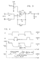
- Fig. 3 shows a circuit schematic for a switched capacitor amplifier.
- Fig. 4 shows clock pulses which control the amplifier of Fig. 3 and pulses generated by the amplifier.
- Fig. 5 shows a circuit schematic of the supply dependent remover.
- Fig. 1 shows a block diagram of the voltage reference generator circuit according to the teachings of the present invention.
- the voltage reference generator circuit includes a threshold difference generator 10, a switched capacitor amplifier 12 and a supply dependent remover 14.
- the threshold difference generator 10 provides a differential voltage V RII at nodes A and B, respectively.
- the differential voltage at node A and node B is a fixed value set by threshold tailoring implant.
- the fixed differential voltage (V RII ) is amplified by switched capacitor amplifier 12 and appears at node C as a voltage level proportional to the amplified V RII .
- Clocks C1 and C2 are used to switch capacitors (to be described hereinafter) in the switched capacitor amplifier.
- the voltage at node C is dependent on the power supply voltage, V DD . This dependency is removed by the supply dependent remover 14, leaving a voltage that is dependent only on V RII . and component matching characteristics.
- Fig. 2 shows a circuit schematic of the threshold difference generator.
- the threshold difference generator is comprised of a pair of N-channel enhancement mode FET devices Q1 and Q2, a matched pair of current sources 16 and 18 and operational amplifier (op amp) 20.
- FET device Q1 is connected in series with current source 16.
- FET device Q2 is connected in series with current source 18.
- the current sources 16 and 18 are connected to the power supply V DD .
- the gate electrode of FET device Q1 is connected to the drain electrode and the drain electrode is connected to the inverting input of operational amplifier 20.
- the drain of FET device Q2 is connected to the positive input of amp 20.
- the differential voltage V RII The differential voltage V RII .
- the threshold voltage of Q1 is maintained at its natural level while the final threshold voltage of device Q2 is tailored so that digital circuit performance is optimized.
- "natural threshold” means the threshold voltage existing before a device is subjected to a threshold tailoring implant process.
- the threshold tailoring is a process step in which ions are implanted to shift the threshold voltage of a device. It should be noted that the threshold shift could have been implemented on Q1 rather than Q2. In other words, the threshold tailoring implant may be practiced on either Q1 or Q2.
- Fig. 3 shows a circuit diagram for the switched capacitor amplifier 12 (Fig. 1.).
- the switched capacitor amplifier is comprised of operational amplifier 22.
- the differential voltage V RII (Fig. 2) is coupled via switches SW1 and SW2, and capacitor C I to the negative terminal of the operational amplifier.
- switch SW1 is driven by clock pulses C1 (Fig. 4) while switch SW2 is driven by the negative phase of clock C1.
- a voltage divider circuit formed from identical series connected resistors R is connected to V DD and form a bias voltage at node V ACG .
- node V ACG is effectively an A.C. ground at voltage level V DD /2.
- the output of operational amplifier 22 is tied to node X and a feedback circuit comprising of capacitor C f and switch SW3 interconnects node X of the operational amplifier to the negative input terminal.
- switch SW4 interconnects node X to capacitor C s and output node C.
- Fig. 4 shows a graphical representation of clock pulses that are used for driving the switches in Fig. 3 and voltage waveforms that are generated at selected nodes of Fig. 3.
- curve A is a representation of clock C1 which is used for driving switch SW1 (Fig. 3).
- curve B represents clock C2 which is used for driving switch SW4 (Fig. 3).
- Curve C is a graphical representation of the voltage waveform which is outputted at node X (Fig. 3).
- curve D shows a graphical representation of the steady state level voltage signal which is outputted at node C (Fig. 3).
- capacitors CI and CF must be periodically reset.
- the resetting procedure is necessary to prevent charge loss due to leakage on capacitors CI and CF, respectively.
- This is done using C1 by closing switch SW3. With switch SW3 closed, CF is shorted, causing node X and the inverting input to operational amplifier 22 to be set at V ACG .
- the voltage at node B is connected to the left plate of capacitor CI via SW2.
- switch SW3 and switch SW2 are opened while switch SW1 is closed.
- the voltage on node A is transferred to the left plate of capacitor C1.
- a graphical representation of ⁇ V out is shown in curve C (Fig. 4). Because there is a finite time for node X (Fig. 3) to settle to its final value, the C2 clock is delayed for a period (T2 - T1) before turning on. This ensures that the node C voltage is free of glitches.
- the voltage at node C is shown in curve D (Fig. 4).
- the voltage may also be described by the following mathematical expression (6)
- V c V DD /2 - (CI/CF) (V A - V B )
- V C V DD /2 -(CI/CF) V RII From (7) it is seen that V C is V DD dependent. This dependency is removed with the circuit of Fig. 5.
- Fig. 5 shows a circuit for removing the V DD component of the output signal.
- the circuit is comprised of voltage follower network 26, currentmirror network 28 and current mirror network 30.
- the voltage follower network 26 includes op amplifier 32 and N-channel FET device Q1.
- the gate of Q1 is connected to the output of op amplifier 32.
- the source of Q1 is tied to the inverting input of op amplifier 32 and to ground via resistor R. The configuration ensures that an input voltage V c appearing at node C is reflected across resistor R.
- the drain electrode of FET device Q1 is tied to current mirror network 28.
- Current mirror network 28 includes P-channel FETs Q2 and Q3.
- the source electrodes of Q2 and Q3 are tied to supply voltage (V DD ).
- the current mirror has a gain of two. Other gain ratios may be used without departing from the spirit and scope of the present invention.
- the gain is achieved by making the width to length (W/L) ratio of Q3 twice the width to length ratio of Q2.
- W/L width to length
- the source electrode of Q3 is tied to current mirror network 30.
- Current mirror network 30 includes N-channel FETs Q4 and Q5.
- the source electrodes of Q4 and Q5 are tied to ground.
- the drain electrode of Q5 is coupled through resistor R to supply voltage V DD and output voltage V o .
- Current mirror 30 has a gain of 1. This is achieved by making the width to length ratio of FET devices Q4 and Q5 identical.
Landscapes
- Engineering & Computer Science (AREA)
- Microelectronics & Electronic Packaging (AREA)
- Physics & Mathematics (AREA)
- Nonlinear Science (AREA)
- Electromagnetism (AREA)
- General Physics & Mathematics (AREA)
- Radar, Positioning & Navigation (AREA)
- Automation & Control Theory (AREA)
- Amplifiers (AREA)
- Control Of Electrical Variables (AREA)
Claims (7)
- Dispositif générateur de tension de référence dans la technologie CMOS, comprenant un premier circuit (10) pour produire une tension différentielle et un second circuit (12) pour amplifier et décaler la tension différentielle afin de délivrer une tension unique, ledit dispositif étant caractérisé en ce qu'il comprend :
un troisième circuit (14) pour supprimer sélectivement les composantes non voulues de ladite tension unique et pour délivrer une tension de référence qui est indépendante de l'alimentation et de la température, comprenant un réseau à charge de tension (26) comportant un noeud d'entrée alimenté avec la tension unique et un noeud de sortie, un premier réseau à miroir de courant (28) ayant un gain d'au moins deux couplé au noeud de sortie et un second réseau à miroir de courant (30) ayant un gain d'au moins un couplant une sortie dudit premier réseau à miroir de-courant à une borne de sortie. - Dispositif selon la revendication 1, comprenant en outre une alimentation (VDD) fonctionnelle dans une plage de tension de 5 volts et la masse, ladite alimentation étant apte à délivrer une puissance d'alimentation auxdits premier (10), second (12) et troisième (14) circuits.
- Dispositif selon la revendication 1 ou 2, dans lequel ledit premier circuit comprend :
un amplificateur opérationnel (20) comportant un noeud de sortie, une entrée inverseuse et une entrée non inverseuse,
un premier réseau de polarisation (18, Q2) couplant le noeud de sortie et l'entrée non inverseuse à un premier et un second niveaux de tension, et
un second réseau de polarisation (16, Q1) couplant l'entrée inverseuse au premier et au second niveaux de tension, d'où il résulte que les premier et second réseaux de polarisation sont connectés en une configuration parallèle avec chaque réseau comportant une source de courant connectée en série à un dispositif FET. - Dispositif selon la revendication 3, dans lequel les sources de courant (18, 16) desdits premier et second réseaux sont identiques et dans lequel les tensions de seuil des dispositifs FET desdits premier et second réseaux sont différentes.
- Dispositif selon l'une quelconque des revendications précédentes, dans lequel ledit second circuit (12) comprend un amplificateur opérationnel (22) comportant une entrée inverseuse, une entrée non inverseuse et un noeud de sortie, un premier moyen de stockage (Ci) connecté à l'entrée inverseuse, un premier moyen d'interrupteur (SW1, SW2) connecté audit premier moyen de stockage, un réseau de polarisation interconnectant l'entrée non inverseuse entre un premier et un second niveaux de tension, un réseau de contre-réaction interconnectant le noeud de sortie à l'entrée inverseuse, un second moyen d'interrupteur (SW4) connecté en série avec le noeud de sortie et un second moyen de stockage (CS) interconnectant ledit second moyen d'interrupteur entre un troisième et un quatrième niveaux de tension.
- Dispositif selon la revendication 5, dans lequel ledit réseau de polarisation du second circuit (12) comprend des résistances identiques connectées en série (R).
- Dispositif selon la revendication 5 ou 6, dans lequel ledit réseau de contre-réaction comprend un condensateur connecté en parallèle avec un interrupteur (SW3).
Applications Claiming Priority (2)
| Application Number | Priority Date | Filing Date | Title |
|---|---|---|---|
| US23189 | 1987-03-06 | ||
| US07/023,189 US4742292A (en) | 1987-03-06 | 1987-03-06 | CMOS Precision voltage reference generator |
Publications (2)
| Publication Number | Publication Date |
|---|---|
| EP0282725A1 EP0282725A1 (fr) | 1988-09-21 |
| EP0282725B1 true EP0282725B1 (fr) | 1992-06-24 |
Family
ID=21813604
Family Applications (1)
| Application Number | Title | Priority Date | Filing Date |
|---|---|---|---|
| EP88101850A Expired EP0282725B1 (fr) | 1987-03-06 | 1988-02-09 | CMOS générateur de tension de référence |
Country Status (4)
| Country | Link |
|---|---|
| US (1) | US4742292A (fr) |
| EP (1) | EP0282725B1 (fr) |
| JP (1) | JPH07111662B2 (fr) |
| DE (1) | DE3872275T2 (fr) |
Cited By (1)
| Publication number | Priority date | Publication date | Assignee | Title |
|---|---|---|---|---|
| US8400374B2 (en) | 2005-12-02 | 2013-03-19 | Semiconductor Energy Laboratory Co., Ltd. | Semiconductor device |
Families Citing this family (35)
| Publication number | Priority date | Publication date | Assignee | Title |
|---|---|---|---|---|
| US4894562A (en) * | 1988-10-03 | 1990-01-16 | International Business Machines Corporation | Current switch logic circuit with controlled output signal levels |
| US5001362A (en) * | 1989-02-14 | 1991-03-19 | Texas Instruments Incorporated | BiCMOS reference network |
| US4943737A (en) * | 1989-10-13 | 1990-07-24 | Advanced Micro Devices, Inc. | BICMOS regulator which controls MOS transistor current |
| JP2715642B2 (ja) * | 1990-08-22 | 1998-02-18 | 日本電気株式会社 | 半導体集積回路 |
| US5059820A (en) * | 1990-09-19 | 1991-10-22 | Motorola, Inc. | Switched capacitor bandgap reference circuit having a time multiplexed bipolar transistor |
| US5109187A (en) * | 1990-09-28 | 1992-04-28 | Intel Corporation | CMOS voltage reference |
| US5047707A (en) * | 1990-11-19 | 1991-09-10 | Motorola, Inc. | Voltage regulator and method for submicron CMOS circuits |
| JP3076097B2 (ja) * | 1991-08-26 | 2000-08-14 | 日本電気株式会社 | 基準電位発生回路 |
| US5451859A (en) * | 1991-09-30 | 1995-09-19 | Sgs-Thomson Microelectronics, Inc. | Linear transconductors |
| US5498952A (en) * | 1991-09-30 | 1996-03-12 | Sgs-Thomson Microelectronics, S.A. | Precise current generator |
| FR2681961A1 (fr) * | 1991-09-30 | 1993-04-02 | Sgs Thomson Microelectronics | Generateur de courant precis. |
| US5390020A (en) * | 1992-09-14 | 1995-02-14 | Eastman Kodak Company | Video amplifier stabilization for CRT printing |
| US5825167A (en) * | 1992-09-23 | 1998-10-20 | Sgs-Thomson Microelectronics, Inc. | Linear transconductors |
| US5668709A (en) * | 1995-03-02 | 1997-09-16 | International Business Machine Corporation | Switched capacitor current source |
| EP0731403A3 (fr) * | 1995-03-08 | 1997-07-23 | Sgs Thomson Microelectronics | Source de courant constante |
| US5703476A (en) * | 1995-06-30 | 1997-12-30 | Sgs-Thomson Microelectronics, S.R.L. | Reference voltage generator, having a double slope temperature characteristic, for a voltage regulator of an automotive alternator |
| GB2308684B (en) * | 1995-12-22 | 2000-03-29 | Motorola Inc | Switched-capacitor reference circuit |
| JPH10260742A (ja) * | 1997-03-19 | 1998-09-29 | Advantest Corp | 精密電圧発生装置 |
| GB2341246A (en) * | 1998-09-03 | 2000-03-08 | Ericsson Telefon Ab L M | Differential level shifting circuit |
| US6222395B1 (en) | 1999-01-04 | 2001-04-24 | International Business Machines Corporation | Single-ended semiconductor receiver with built in threshold voltage difference |
| US6466081B1 (en) | 2000-11-08 | 2002-10-15 | Applied Micro Circuits Corporation | Temperature stable CMOS device |
| US6434049B1 (en) * | 2000-12-29 | 2002-08-13 | Intel Corporation | Sample and hold voltage reference source |
| US6570789B2 (en) | 2000-12-29 | 2003-05-27 | Intel Corporation | Load for non-volatile memory drain bias |
| US6744671B2 (en) * | 2000-12-29 | 2004-06-01 | Intel Corporation | Kicker for non-volatile memory drain bias |
| US6535423B2 (en) | 2000-12-29 | 2003-03-18 | Intel Corporation | Drain bias for non-volatile memory |
| US6456540B1 (en) | 2001-01-30 | 2002-09-24 | Intel Corporation | Method and apparatus for gating a global column select line with address transition detection |
| CN100449594C (zh) * | 2003-04-25 | 2009-01-07 | 株式会社半导体能源研究所 | 半导体装置 |
| EP1624358B1 (fr) * | 2003-05-14 | 2015-03-11 | Semiconductor Energy Laboratory Co., Ltd. | Dispositif semi-conducteur |
| CN1802681B (zh) * | 2003-06-06 | 2011-07-13 | 株式会社半导体能源研究所 | 半导体装置 |
| JP4681983B2 (ja) * | 2005-08-19 | 2011-05-11 | 富士通セミコンダクター株式会社 | バンドギャップ回路 |
| EP2169824A1 (fr) * | 2008-09-25 | 2010-03-31 | Moscad Design & Automation Sàrl | Circuit amplificateur d'erreurs de condensateur commuté pour la génération d'une référence de courant de précision ou pour une utilisation dans un oscillateur de précision |
| US7852252B2 (en) * | 2008-12-31 | 2010-12-14 | Intel Corporation | Single-ended to differential amplification and pipeline analog-to-digital conversion for digitally controlled DC-DC converters |
| JP5515708B2 (ja) * | 2009-12-11 | 2014-06-11 | 富士通株式会社 | バイアス回路及びそれを有する増幅回路 |
| CN104536510B (zh) * | 2014-11-18 | 2016-04-20 | 中山大学 | 一种差分电压转电流电路 |
| CN107463201B (zh) * | 2017-08-02 | 2018-10-19 | 中国电子科技集团公司第二十四研究所 | 一种电压转电流电路及装置 |
Family Cites Families (11)
| Publication number | Priority date | Publication date | Assignee | Title |
|---|---|---|---|---|
| US3975648A (en) * | 1975-06-16 | 1976-08-17 | Hewlett-Packard Company | Flat-band voltage reference |
| US4100437A (en) * | 1976-07-29 | 1978-07-11 | Intel Corporation | MOS reference voltage circuit |
| JPS5342141U (fr) * | 1976-09-17 | 1978-04-11 | ||
| CH628462A5 (fr) * | 1978-12-22 | 1982-02-26 | Centre Electron Horloger | Source de tension de reference. |
| FR2447610A1 (fr) * | 1979-01-26 | 1980-08-22 | Commissariat Energie Atomique | Generateur de tension de reference et circuit de mesure de la tension de seuil d'un transistor mos, applicable a ce generateur de tension de reference |
| US4346344A (en) * | 1979-02-08 | 1982-08-24 | Signetics Corporation | Stable field effect transistor voltage reference |
| JPS55138322U (fr) * | 1979-03-22 | 1980-10-02 | ||
| JPS57157313A (en) * | 1981-03-23 | 1982-09-28 | Nec Corp | Integrated semiconductor device |
| US4374357A (en) * | 1981-07-27 | 1983-02-15 | Motorola, Inc. | Switched capacitor precision current source |
| US4464588A (en) * | 1982-04-01 | 1984-08-07 | National Semiconductor Corporation | Temperature stable CMOS voltage reference |
| JPS58187015A (ja) * | 1982-04-26 | 1983-11-01 | Nippon Telegr & Teleph Corp <Ntt> | スイツチト・キヤパシタ回路 |
-
1987
- 1987-03-06 US US07/023,189 patent/US4742292A/en not_active Expired - Fee Related
-
1988
- 1988-02-09 DE DE8888101850T patent/DE3872275T2/de not_active Expired - Fee Related
- 1988-02-09 EP EP88101850A patent/EP0282725B1/fr not_active Expired
- 1988-02-10 JP JP63027815A patent/JPH07111662B2/ja not_active Expired - Lifetime
Cited By (1)
| Publication number | Priority date | Publication date | Assignee | Title |
|---|---|---|---|---|
| US8400374B2 (en) | 2005-12-02 | 2013-03-19 | Semiconductor Energy Laboratory Co., Ltd. | Semiconductor device |
Also Published As
| Publication number | Publication date |
|---|---|
| JPS63229509A (ja) | 1988-09-26 |
| JPH07111662B2 (ja) | 1995-11-29 |
| US4742292A (en) | 1988-05-03 |
| DE3872275D1 (de) | 1992-07-30 |
| EP0282725A1 (fr) | 1988-09-21 |
| DE3872275T2 (de) | 1993-01-07 |
Similar Documents
| Publication | Publication Date | Title |
|---|---|---|
| EP0282725A1 (fr) | CMOS générateur de tension de référence | |
| EP0778510B1 (fr) | Source de courant bidirectionnelle à haute symétrie | |
| US5087891A (en) | Current mirror circuit | |
| US4622480A (en) | Switched capacitor circuit with high power supply projection ratio | |
| EP0701321B1 (fr) | Circuit et méthode de suppression de courant de fuite dans un dispositif analogue | |
| US5565813A (en) | Apparatus for a low voltage differential amplifier incorporating switched capacitors | |
| KR0134661B1 (ko) | 전위전류 변환기 | |
| US5959446A (en) | High swing current efficient CMOS cascode current mirror | |
| US4874969A (en) | High speed CMOS comparator with hysteresis | |
| US5057722A (en) | Delay circuit having stable delay time | |
| EP0158646B1 (fr) | Circuits a condensateurs commutes | |
| EP0301184B1 (fr) | Générateur de tension de référence CMOS | |
| JPH10240849A (ja) | 低電圧mosfetを持つ電流ミラーを使用した積算機及び神経網シナプス | |
| JPH06252664A (ja) | カスコード電流ミラーを具える集積回路 | |
| US6400219B1 (en) | High-speed offset comparator | |
| KR19990047008A (ko) | 외부조건 변화에 둔감한 기준전압 발생회로 | |
| US4961015A (en) | MOS current switching circuit | |
| EP0654903B1 (fr) | Circuits d'attaque | |
| US6100738A (en) | High-speed current switch with complementary stages | |
| JPH11272786A (ja) | 差動増幅回路 | |
| EP0784824B1 (fr) | Integrateur de courant | |
| CA2513956A1 (fr) | Circuit de temperature reglable et programmable a coefficient de temperature proportionnel a absolu | |
| KR950016002A (ko) | 3치 입력 버퍼 회로 | |
| WO1996038912A1 (fr) | Circuit a retard variable | |
| EP0483125B1 (fr) | Source de courant |
Legal Events
| Date | Code | Title | Description |
|---|---|---|---|
| PUAI | Public reference made under article 153(3) epc to a published international application that has entered the european phase |
Free format text: ORIGINAL CODE: 0009012 |
|
| AK | Designated contracting states |
Kind code of ref document: A1 Designated state(s): DE FR GB IT |
|
| 17P | Request for examination filed |
Effective date: 19890117 |
|
| 17Q | First examination report despatched |
Effective date: 19901116 |
|
| GRAA | (expected) grant |
Free format text: ORIGINAL CODE: 0009210 |
|
| AK | Designated contracting states |
Kind code of ref document: B1 Designated state(s): DE FR GB IT |
|
| PG25 | Lapsed in a contracting state [announced via postgrant information from national office to epo] |
Ref country code: IT Free format text: LAPSE BECAUSE OF FAILURE TO SUBMIT A TRANSLATION OF THE DESCRIPTION OR TO PAY THE FEE WITHIN THE PRE;WARNING: LAPSES OF ITALIAN PATENTS WITH EFFECTIVE DATE BEFORE 2007 MAY HAVE OCCURRED AT ANY TIME BEFORE 2007. THE CORRECT EFFECTIVE DATE MAY BE DIFFERENT FROM THE ONE RECORDED.SCRIBED TIME-LIMIT Effective date: 19920624 |
|
| REF | Corresponds to: |
Ref document number: 3872275 Country of ref document: DE Date of ref document: 19920730 |
|
| ET | Fr: translation filed | ||
| PLBE | No opposition filed within time limit |
Free format text: ORIGINAL CODE: 0009261 |
|
| 26N | No opposition filed | ||
| PGFP | Annual fee paid to national office [announced via postgrant information from national office to epo] |
Ref country code: FR Payment date: 19950128 Year of fee payment: 8 |
|
| PGFP | Annual fee paid to national office [announced via postgrant information from national office to epo] |
Ref country code: DE Payment date: 19950223 Year of fee payment: 8 |
|
| PG25 | Lapsed in a contracting state [announced via postgrant information from national office to epo] |
Ref country code: FR Effective date: 19961031 |
|
| PG25 | Lapsed in a contracting state [announced via postgrant information from national office to epo] |
Ref country code: DE Effective date: 19961101 |
|
| REG | Reference to a national code |
Ref country code: FR Ref legal event code: ST |
|
| PGFP | Annual fee paid to national office [announced via postgrant information from national office to epo] |
Ref country code: GB Payment date: 19970120 Year of fee payment: 10 |
|
| PG25 | Lapsed in a contracting state [announced via postgrant information from national office to epo] |
Ref country code: GB Free format text: LAPSE BECAUSE OF NON-PAYMENT OF DUE FEES Effective date: 19980209 |
|
| GBPC | Gb: european patent ceased through non-payment of renewal fee |
Effective date: 19980209 |