EP0283593A1 - Amplificateur vidéo - Google Patents
Amplificateur vidéo Download PDFInfo
- Publication number
- EP0283593A1 EP0283593A1 EP87200538A EP87200538A EP0283593A1 EP 0283593 A1 EP0283593 A1 EP 0283593A1 EP 87200538 A EP87200538 A EP 87200538A EP 87200538 A EP87200538 A EP 87200538A EP 0283593 A1 EP0283593 A1 EP 0283593A1
- Authority
- EP
- European Patent Office
- Prior art keywords
- transistor
- current source
- transistors
- circuit
- current
- Prior art date
- Legal status (The legal status is an assumption and is not a legal conclusion. Google has not performed a legal analysis and makes no representation as to the accuracy of the status listed.)
- Withdrawn
Links
Images




Classifications
-
- H—ELECTRICITY
- H03—ELECTRONIC CIRCUITRY
- H03F—AMPLIFIERS
- H03F3/00—Amplifiers with only discharge tubes or only semiconductor devices as amplifying elements
- H03F3/189—High-frequency amplifiers, e.g. radio frequency amplifiers
- H03F3/19—High-frequency amplifiers, e.g. radio frequency amplifiers with semiconductor devices only
-
- H—ELECTRICITY
- H03—ELECTRONIC CIRCUITRY
- H03F—AMPLIFIERS
- H03F3/00—Amplifiers with only discharge tubes or only semiconductor devices as amplifying elements
- H03F3/42—Amplifiers with two or more amplifying elements having their DC paths in series with the load, the control electrode of each element being excited by at least part of the input signal, e.g. so-called totem-pole amplifiers
-
- H—ELECTRICITY
- H03—ELECTRONIC CIRCUITRY
- H03F—AMPLIFIERS
- H03F3/00—Amplifiers with only discharge tubes or only semiconductor devices as amplifying elements
- H03F3/45—Differential amplifiers
- H03F3/45071—Differential amplifiers with semiconductor devices only
- H03F3/45076—Differential amplifiers with semiconductor devices only characterised by the way of implementation of the active amplifying circuit in the differential amplifier
- H03F3/4508—Differential amplifiers with semiconductor devices only characterised by the way of implementation of the active amplifying circuit in the differential amplifier using bipolar transistors as the active amplifying circuit
- H03F3/45085—Long tailed pairs
- H03F3/45089—Non-folded cascode stages
-
- H—ELECTRICITY
- H04—ELECTRIC COMMUNICATION TECHNIQUE
- H04N—PICTORIAL COMMUNICATION, e.g. TELEVISION
- H04N5/00—Details of television systems
- H04N5/14—Picture signal circuitry for video frequency region
- H04N5/148—Video amplifiers
Definitions
- the present invention relates to a broadband amplifier such as a videoamplifier.
- the amplifier may have a hard switching characteristic.
- videoamplifiers with a linear characteristic have been used.
- the large signal behaviour of conventional linear amplifiers has proved not to be satisfactory in certain applications.
- the output signal cannot keep up with the rise of the input signal, because the output voltage of such a videoamplifier is only increased with a limited slew rate.
- the output signal will reach the desired voltage level only after a certain rise time.
- the signal that has to be amplified is a pulse signal which has a pulse width in the order of or even smaller than said rise time, the output signal will not be able to reach its full amplitude. Consequently, the band-width of the amplifier is practically limited by the rise time.
- At least one transistor amplifying circuit is designed in such a way that the transistors exhibit a linear characteristic in a range of small variations of the input signal and a hard switching characteristic in the range of large input signal variations. Due to the hard switching characteristics of the transistors, the slew rate of the amplifier is increased and the rise time of the output signal in response to a large stepwise rise of the input signal is reduced. On the other hand, when the variation of the input signal is small or when the input signal is substantially constant after a large stepwise rise, the linear characteristic is predominant so that the output signal is kept at the desired level proportional to the input level.
- a videoamplifier according to the invention is capable of amplifying for instance a pulse-like video signal the amplitude of which varies between sixteen distinct values corresponding to sixteen picture half-tones. Even if the frequency of the input signal is as large as for instance 150 to 200 MHz, the maximal rise time of the output signal will be smaller than the pulse width so that all sixteen output levels will be fairly distinguishable from each other.
- a useful amplifying circuit which provides the desired amplifying characteristic is specified in claim 2.
- the subclaims relate to more specific features of the amplifying circuit which lead to a simple low-cost circuit construction and to a reduction of energy dissipation.
- an amplifying circuit includes a constant current source 10 connected to a branched circuit 12 which has first and second parallel branches 14, 16 connected in series to the current source 10.
- the first branch 14 includes a transistor T1 which has its collector connected to a positive voltage terminal (+).
- the input voltage V i of the amplifying circuit is supplied to the base of the transistor T1.
- the second branch 16 includes a transistor T2, the collector of which is connected to another constant current source 18.
- the output voltage V o is picked up at a point between the current source 18 and the transistor T2.
- a capacitive load applied to the output of the amplifying circuit is represented by a capacitor C.
- a feedback circuit 20 for controlling the base voltage V b2 of the transistor T2 comprises a resistor R1 connected between the collector and the base of the transistor T2 and a resistor R2 and a capacitor C2 connected in parallel between the base of the transistor T2 and ground.
- the transistors T1 and T2 are of the same type, and the current I2 flowing through the current source 18 is one half of the current I tail flowing through the current source 10. Consequently, the current I1 flowing through the transistor T1 is equal to I2, and the voltage V b2 is normally equal to V i .
- the voltage V b2 changes in accordance with V i . If, for instance, the input voltage V i is increased, the base-emitter voltage drop across the transistor T2 is reduced so that the emitter voltages V e of both transistors T1, T2 become larger. As the base-emitter voltage of the transistor T2 tends to be reduced, the voltage drop across the transistor T2 and consequently the output voltage V o is increased. The base voltage V b2 of the transistor T2 is increased due to the effect of the voltage dividing resistors R1, R2. Thus, a new equilibrium is reached as soon as V b2 equals the new level of the input voltage V i .
- the feedback circuit 20 increases the base voltage V b2 of the transistor T2 only with a certain delay which in the present example is determined by the capacity of the capacitors C and C2.
- the transitors T1 and T2 behave like switches.
- the transitor T1 is fully opened while the transistor T2 is fully closed. Consequently, the complete current I2 is available for charging the load capacitor C. This results in a superproportional increase of the output voltage V o .
- V max the band-width
- I2/C tot (1/2)I tail /C tot
- f(-3dB) (1/2)I tail . ⁇ 2/(2 ⁇ C tot V max ).
- the band-width f(-3dB) is as large as 150MHz.
- C2 should be adjusted so as to optimize the small signal behaviour. Considering a straight frequency curve, C2 should be in the order of (C + C c ).2.re.A.(1/R1 + 1/R2) + C c .R1/R2 wherein C c is the collector-base capacity and re is the emitter impedance (U BE /I C ) of the transistor T2 and A is the amplification factor.
- Fig. 2 shows a modified amplifier circuit wherein the transistor T2 has been replaced by a series connection of two transistors T21, T22.
- the resistor R1 has been replaced by a series connection of two resistors R11, R12.
- the base of the transistor T22 is connected to a point between the resistors R11 and R12.
- a capacitor C3 for compensating the influence of the collector-base capacity C c of the transistor T21 is connected in parallel to resistor R11 and has a capacity value substantially equal to C c .
- the current source 10 is formed by a transistor T3 and an emitter resistor R3 which is connected to a negative voltage terminal -V1.
- the base of the transistor T3 is connected to another negative voltage terminal -V2.
- the current source 18 is formed by a series connection of two transistors T41, T42 and an emitter resistor R4 connected to a positive voltage terminal +V3.
- the base of transistor T42 is connected to a positive voltage terminal +V4.
- the base of the transistor T41 is connected to the voltage terminal +V4 and to the output terminal V o via resistors R5 and R6 respectively.
- a capacitor C4 is connected in parallel with the resistor R5 and has a capacity value substantially equal to the capacity C c of the transistor T42.
- the purpose of providing series of transistors T21, T22 and T41, T42 instead of single transistors is to reduce the power dissipation and the collector-emitter tension of each transistor.
- the emitter current gain ⁇ (h FE ) is about 50.
- the transistors T41 and T42 are pnp-transistors, that also have a small collector-base capacity substantially equal to that of the transistors T21, T22.
- the voltage -V1 is in the order of -5V while the voltage +V3 is about 35V.
- the resistance of the resistors R11, R12, R5 and R6 is about 1k ⁇ and the resistance of R2 is about 100 ⁇ . If the input voltage V i varies in a range of 0,1 to 1,1V, the output voltage V o is in the range of approximately 5 to 25V.
- the current I tail is about 80mA and the output capacity C is about 4pF.
- the capacity C2 is approximately 50pF.
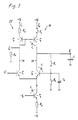
- FIG. 3 A different embodiment of the invention is illustrated in Fig. 3. This embodiment is different from the previosly described embodiment in that the collector of the transistor T1 is connected to another current source 22 formed by a pnp-transistor T5 and an emitter resistor R6 connected to the positive voltage terminal +V3.
- the collector of the transistor T5 is directly connected to the base of this transistor and is further connected to ground via a resistor R7 which has a comparatively high resistance or even can be omitted.
- the current source 18 is formed by a single transistor T6 the base of which is directly coupled to the base of the transistor T5.
- the transistor T1 opens, the base voltage of the transistor T5 drops so that the current I1 delivered by the current source 22 increases.
- the current sources 18 and 22 are interlocked with each other due to the common potential of the bases of the transistors T6 and T5, the increase of the current I1 is reflected by a like increase of the current I2.
- I2 becomes equal to I tail .
- the slew rate is twice as high as in the first embodiment.
- the single transistor T2 is again replaced by a series of transistors.
- the current source 22 includes a transistor T7 interposed between the collector of the transistor T5 and the connecting point of the resistor R7.
- the base of the transistor T7 is connected to a constant voltage terminal +V4.
- the current source 18 comprises the transistor T6 described in conjunction with Fig. 3 and transistors T41 and T42 which may be compared to the transistors T41 and T42 in Fig. 2.
- the base of the transistor T42 is connected to a positive voltage terminal +V5 the voltage of which is smaller than V3 but larger than V4.
- FIG. 5 shows another modification of the circuit according to Fig. 3.
- additional transistors T8 and T9 are connected in series between the transistors T2 and T6.
- Another additional transistor T10 is interposed between the transistors T1 and T5.
- the bases of the transistors T8 and T10 are connected to a constant voltage terminal +V4, and the base of the transistor T9 is connected to another constant voltage terminal +V5.
- a capacitor C1 is connected in parallel with the resistor R1.
- the resistor R7 (Fig. 3) is removed.
- the voltage -V1 has a value of about -5V
- the voltage +V3 has a value of about +42V.
- the voltages at the terminals +V4 and +V5 are selected in such a manner that the transistors T8, T9 and T10 are not saturated.
- the voltage at the terminal +V4 is set to +4V
- the voltage at the terminal +V5 is set to +38V. Accordingly, the voltage drop across the transistors T1, T2 and across the transistors T5, T6 is comparatively small.
- the collector-base capacitance of a transistor is dependent on the collector-base voltage V CB .
- the circuit according to Fig. 5 has the advantage that the collector-base capacitance C c of the transistors T1, T2 and T6 is almost constant, so that the influence of changes of the input and output voltages on the collector-base capacitance and hence on the frequency curve of the amplifier is eliminated. Specifically, when the output voltage V o changes, the collector-base capacitance C c of the transistor T2 and, consequently, the input capacitance C in of this transistor is almost constant. The sum of the collector-base capacitances C c of the transistors T8 and T9 is constant as well. Thus, the frequency curve of the amplifying circuit is fixed by the constant values of R1, C1, R2, C2 and C in .
- the capacitor C1 is provided in order to make the proper selection of the capacitor C2 less critical.
- the value of the capacitance C1 should be chosen as low as possible and practical.
- a straight frequency curve is obtained if C2 + C in ⁇ C1 .
- R1/R2 In a practical example, C has a value of 4pF, C c has a value of 1 to 2pF, and C1 is set to 1pF, while C2 is set to about 6 to 12pF.
- the total output capacitance C tot is given by The transistors T9 and T10 prevent large changes of the collector-base voltages of the transistors T6 and T1, respecively, so that the collector-base capacitances C c of the transistors T6 and T1 are also substantially constant.
- the transistors T8, T9 and T10 dissipate the largest part of the power, so that the transistors T1, T2, T5 and T6 have only low power dissipations (e.g. smaller than 1 watt). This has the advantage that the temperature offset of these transistors is reduced.
Landscapes
- Engineering & Computer Science (AREA)
- Power Engineering (AREA)
- Multimedia (AREA)
- Signal Processing (AREA)
- Amplifiers (AREA)
- Picture Signal Circuits (AREA)
Priority Applications (3)
| Application Number | Priority Date | Filing Date | Title |
|---|---|---|---|
| EP87200538A EP0283593A1 (fr) | 1987-03-25 | 1987-03-25 | Amplificateur vidéo |
| US07/172,011 US4859962A (en) | 1987-03-25 | 1988-03-23 | Videoamplifier |
| JP63069200A JPS63260366A (ja) | 1987-03-25 | 1988-03-23 | ビデオ増幅器 |
Applications Claiming Priority (1)
| Application Number | Priority Date | Filing Date | Title |
|---|---|---|---|
| EP87200538A EP0283593A1 (fr) | 1987-03-25 | 1987-03-25 | Amplificateur vidéo |
Publications (1)
| Publication Number | Publication Date |
|---|---|
| EP0283593A1 true EP0283593A1 (fr) | 1988-09-28 |
Family
ID=8197596
Family Applications (1)
| Application Number | Title | Priority Date | Filing Date |
|---|---|---|---|
| EP87200538A Withdrawn EP0283593A1 (fr) | 1987-03-25 | 1987-03-25 | Amplificateur vidéo |
Country Status (3)
| Country | Link |
|---|---|
| US (1) | US4859962A (fr) |
| EP (1) | EP0283593A1 (fr) |
| JP (1) | JPS63260366A (fr) |
Cited By (2)
| Publication number | Priority date | Publication date | Assignee | Title |
|---|---|---|---|---|
| EP0643479A1 (fr) * | 1993-09-15 | 1995-03-15 | Plessey Semiconductors Limited | Dispositifs de circuit pré-amplificateur |
| EP0750393A3 (fr) * | 1995-06-24 | 1998-02-25 | Motorola, Inc. | Un étage de sortie d'un amplificateur opérationnel haute tension |
Families Citing this family (1)
| Publication number | Priority date | Publication date | Assignee | Title |
|---|---|---|---|---|
| US5075582A (en) * | 1989-03-30 | 1991-12-24 | Siemens Aktiengesellschaft | Integratable bandpass filter circuit |
Citations (2)
| Publication number | Priority date | Publication date | Assignee | Title |
|---|---|---|---|---|
| US3689848A (en) * | 1970-05-04 | 1972-09-05 | Us Navy | Voltage-to-current converter |
| US4414574A (en) * | 1980-12-23 | 1983-11-08 | Electrohome Limited | Video amplifier with blank stretching |
Family Cites Families (1)
| Publication number | Priority date | Publication date | Assignee | Title |
|---|---|---|---|---|
| US4393355A (en) * | 1981-10-26 | 1983-07-12 | Motorola, Inc. | Operational amplifier |
-
1987
- 1987-03-25 EP EP87200538A patent/EP0283593A1/fr not_active Withdrawn
-
1988
- 1988-03-23 JP JP63069200A patent/JPS63260366A/ja active Pending
- 1988-03-23 US US07/172,011 patent/US4859962A/en not_active Expired - Lifetime
Patent Citations (2)
| Publication number | Priority date | Publication date | Assignee | Title |
|---|---|---|---|---|
| US3689848A (en) * | 1970-05-04 | 1972-09-05 | Us Navy | Voltage-to-current converter |
| US4414574A (en) * | 1980-12-23 | 1983-11-08 | Electrohome Limited | Video amplifier with blank stretching |
Cited By (3)
| Publication number | Priority date | Publication date | Assignee | Title |
|---|---|---|---|---|
| EP0643479A1 (fr) * | 1993-09-15 | 1995-03-15 | Plessey Semiconductors Limited | Dispositifs de circuit pré-amplificateur |
| US5543979A (en) * | 1993-09-15 | 1996-08-06 | Plessey Semiconductors Limited | Preamplifier circuit arrangements for common current flow in a transducer |
| EP0750393A3 (fr) * | 1995-06-24 | 1998-02-25 | Motorola, Inc. | Un étage de sortie d'un amplificateur opérationnel haute tension |
Also Published As
| Publication number | Publication date |
|---|---|
| US4859962A (en) | 1989-08-22 |
| JPS63260366A (ja) | 1988-10-27 |
Similar Documents
| Publication | Publication Date | Title |
|---|---|---|
| US4608502A (en) | I2 L gate circuit arrangement having a switchable current source | |
| US4983927A (en) | Integrated audio amplifier with combined regulation of the "mute" and "standby" functions and the switching transients | |
| US4498057A (en) | Power amplifier with power supply switching | |
| US4509021A (en) | Circuit for amplifying and/or attenuating a signal | |
| US4256980A (en) | Electronic switchover circuit | |
| JPH05129915A (ja) | 漏話防止多入力単一出力アナログスイツチ回路 | |
| US4642482A (en) | Level-shifting circuit | |
| US4218662A (en) | Circuit arrangement for optional dynamic compression or expansion | |
| US4063185A (en) | Direct coupling type power amplifier circuit | |
| US4255716A (en) | Automatic gain control circuit | |
| US6400933B1 (en) | Amplifier | |
| AU559556B2 (en) | A circuit for a high impedance signal source | |
| EP0732807B1 (fr) | Dispositif de filtrage réglable | |
| EP0283593A1 (fr) | Amplificateur vidéo | |
| US4460876A (en) | Low consumption, wide-band linear amplifier operating in sliding class A | |
| EP0406964B1 (fr) | Circuit d'amplification | |
| US4462000A (en) | Amplifier comprising means for eliminating direct voltage transients on the amplifier output | |
| US5166983A (en) | Mute circuit for audio amplifiers | |
| US4069461A (en) | Amplifier circuit having two negative feedback circuits | |
| JPH0519323B2 (fr) | ||
| US4426626A (en) | Signal switching circuit | |
| US4513253A (en) | Electronic amplifier having a transmission factor that is variable by means of a controllable voltage, specifically an expander | |
| US3421100A (en) | Direct coupled amplifier including twostage automatic gain control | |
| US3416094A (en) | Automatic gain control system | |
| GB2074410A (en) | Variable emitter degeneration gain-controlled amplifier |
Legal Events
| Date | Code | Title | Description |
|---|---|---|---|
| PUAI | Public reference made under article 153(3) epc to a published international application that has entered the european phase |
Free format text: ORIGINAL CODE: 0009012 |
|
| AK | Designated contracting states |
Kind code of ref document: A1 Designated state(s): AT BE CH DE ES FR GB GR IT LI LU NL SE |
|
| RBV | Designated contracting states (corrected) |
Designated state(s): BE DE FR GB IT NL SE |
|
| 17P | Request for examination filed |
Effective date: 19890314 |
|
| 17Q | First examination report despatched |
Effective date: 19910213 |
|
| STAA | Information on the status of an ep patent application or granted ep patent |
Free format text: STATUS: THE APPLICATION IS DEEMED TO BE WITHDRAWN |
|
| 18D | Application deemed to be withdrawn |
Effective date: 19911204 |
|
| RIN1 | Information on inventor provided before grant (corrected) |
Inventor name: SIMONS, JOHANNES MATHIEU MARIE Inventor name: MICHELS, CASPER PAUL MATHILDE |