EP0283842A1 - Convertisseur à découpage et récupération - Google Patents
Convertisseur à découpage et récupération Download PDFInfo
- Publication number
- EP0283842A1 EP0283842A1 EP88103635A EP88103635A EP0283842A1 EP 0283842 A1 EP0283842 A1 EP 0283842A1 EP 88103635 A EP88103635 A EP 88103635A EP 88103635 A EP88103635 A EP 88103635A EP 0283842 A1 EP0283842 A1 EP 0283842A1
- Authority
- EP
- European Patent Office
- Prior art keywords
- circuit
- converter
- output
- voltage
- winding
- Prior art date
- Legal status (The legal status is an assumption and is not a legal conclusion. Google has not performed a legal analysis and makes no representation as to the accuracy of the status listed.)
- Granted
Links
- 238000004804 winding Methods 0.000 claims description 32
- 239000003990 capacitor Substances 0.000 claims description 19
- 230000000903 blocking effect Effects 0.000 abstract description 15
- 238000004891 communication Methods 0.000 abstract description 3
- 238000005516 engineering process Methods 0.000 abstract description 2
- 238000009499 grossing Methods 0.000 description 5
- 230000005347 demagnetization Effects 0.000 description 3
- 238000005265 energy consumption Methods 0.000 description 2
- 230000001105 regulatory effect Effects 0.000 description 2
- 230000001276 controlling effect Effects 0.000 description 1
- 238000011161 development Methods 0.000 description 1
- 230000018109 developmental process Effects 0.000 description 1
- 230000005669 field effect Effects 0.000 description 1
- 230000006870 function Effects 0.000 description 1
- 238000002955 isolation Methods 0.000 description 1
- 238000000034 method Methods 0.000 description 1
- 229920006395 saturated elastomer Polymers 0.000 description 1
- 239000004065 semiconductor Substances 0.000 description 1
- 230000001360 synchronised effect Effects 0.000 description 1
Images

Classifications
-
- H—ELECTRICITY
- H02—GENERATION; CONVERSION OR DISTRIBUTION OF ELECTRIC POWER
- H02M—APPARATUS FOR CONVERSION BETWEEN AC AND AC, BETWEEN AC AND DC, OR BETWEEN DC AND DC, AND FOR USE WITH MAINS OR SIMILAR POWER SUPPLY SYSTEMS; CONVERSION OF DC OR AC INPUT POWER INTO SURGE OUTPUT POWER; CONTROL OR REGULATION THEREOF
- H02M3/00—Conversion of DC power input into DC power output
- H02M3/22—Conversion of DC power input into DC power output with intermediate conversion into AC
- H02M3/24—Conversion of DC power input into DC power output with intermediate conversion into AC by static converters
- H02M3/28—Conversion of DC power input into DC power output with intermediate conversion into AC by static converters using discharge tubes with control electrode or semiconductor devices with control electrode to produce the intermediate AC
- H02M3/325—Conversion of DC power input into DC power output with intermediate conversion into AC by static converters using discharge tubes with control electrode or semiconductor devices with control electrode to produce the intermediate AC using devices of a triode or a transistor type requiring continuous application of a control signal
- H02M3/335—Conversion of DC power input into DC power output with intermediate conversion into AC by static converters using discharge tubes with control electrode or semiconductor devices with control electrode to produce the intermediate AC using devices of a triode or a transistor type requiring continuous application of a control signal using semiconductor devices only
- H02M3/33561—Conversion of DC power input into DC power output with intermediate conversion into AC by static converters using discharge tubes with control electrode or semiconductor devices with control electrode to produce the intermediate AC using devices of a triode or a transistor type requiring continuous application of a control signal using semiconductor devices only having more than one ouput with independent control
Definitions
- the invention relates to a converter circuit with a flyback converter as specified in the preamble of patent claim 1.
- This converter circuit contains a regulator that regulates the output voltage of the secondary circuit directly or indirectly.
- An actual value supplied to the controller can be the output voltage of the secondary circuit or the output voltage of an auxiliary circuit simulated by the secondary circuit and connected to an auxiliary winding of the transformer.
- the EMF control has the advantage that the electrical isolation of the secondary circuit and controller is realized with the help of the transformer.
- Power supply devices are required to supply communication systems, which are generally intended to supply several output voltages of different sizes and polarities with narrow tolerances between idle and full load. In many cases, these power supply devices are designed as flow converters or flyback converters according to the known principles.
- the energy consumption on the primary side coincides with the energy output on the secondary side.
- the polarity of the voltage on the transformer swings. This makes the diode in the output circuit conductive. The energy stored in the transformer during the lead phase is delivered to the load. At the same time, the smoothing capacitor is charged again.
- DC converters with the aid of which several output voltages are generated, can be provided with an EMF control and post-regulators can be provided in at least some of the output circuits.
- EMF control the output voltage of an auxiliary winding of the transformer is tapped as the actual value and compared in the regulation and control with the single setpoint of a common setpoint generator.
- the wiring of this auxiliary winding is the same as for the secondary windings for the output voltages.
- the object of the invention is to design a converter circuit as specified in the preamble of patent claim 1 in such a way that it manages with a comparatively low outlay for readjustment.
- the converter circuit for solving this problem is designed in the manner specified in the characterizing part of patent claim 1.
- the rectifier diode and the controllable switch can be arranged in the same or in different longitudinal branches.
- the controllable switch can in particular be a semiconductor switch, preferably a power field effect transistor.
- the measures according to claim 2 have the advantage that the effort of the switching regulator is particularly low. In particular, neither a clock generator nor a pulse width modulator are required. This advantage is particularly significant if, in addition to an output with a comparatively high voltage, the converter circuit has a plurality of outputs provided with post-regulators for relatively low voltages and / or comparatively large currents.
- the winding direction of the secondary winding of the transformer in question can be arbitrary.
- the measures specified in claim 1 have the advantage that the converter circuit combines the advantages of a flyback converter with those of a flow converter.
- the converter circuit shown in FIG. 1 is fed with the input voltage U1.
- the capacitor 1 connected to the input voltage U1 is connected to the primary winding 3a of the transformer 3 via the electronic switch 2.
- Parallel to the first secondary winding 3b of the transformer 3 is a series circuit consisting of the diode 4 and the charging capacitor 5.
- the resistance 6 and the output for the first output voltage U21 are the base load.
- the transformer 3 with said primary circuit 3a and the first secondary circuit 3b forms a flyback converter.
- This blocking converter has an arrangement for EMF control Mistake.
- the control arrangement contains an auxiliary circuit connected to the auxiliary winding 3c of the transformer 3, which is modeled on the first secondary circuit.
- the auxiliary circuit contains the series circuit consisting of the diode 11 and the charging capacitor 10 and connected to the auxiliary winding 3c.
- the voltage divider 9 is parallel to the capacitor 10. The voltage divider 9 is used to generate an auxiliary voltage which is proportional to the open circuit voltage of the flyback converter.
- controller 8 a variable corresponding to the control deviation is formed from a reference voltage and the auxiliary voltage and is fed to pulse width modulator 7.
- the pulse width modulator 7 controls the electronic switch 2 such that the EMF or. Open-circuit voltage of the blocking converter is kept at least approximately at a constant value.
- the EMF control is optimized for the output circuit A1.
- a regulation can optionally be provided which uses the output voltage U21 to be regulated to a constant value as the actual value.
- the converter circuit is provided with several further secondary circuits A2 and A3. These secondary circuits each contain a switching post-regulator that regulates the output voltage U22 or U23 of the secondary circuit to a constant value.
- a series circuit comprising the rectifier diode 13, the transistor 12 and the freewheeling diode 14 connected in series with the opposite polarity is connected to the further secondary winding 3d.
- Parallel to the freewheeling diode 14 is the filter circuit consisting of the choke 15 and the capacitor 17.
- the output for the further output voltage U22 and the voltage divider 18 are parallel to the capacitor 17.
- the tap of the voltage divider 18 is routed to the controller 16.
- the controller 16 controls the transistor 12 via the pulse width modulator 20.
- the pulse width modulator 20 is synchronized by the clock generator 19, which is connected to the secondary winding 3d.
- the secondary circuit A3 connected to the further secondary winding 3e for generating the output voltage U23 is constructed in the same way as the secondary circuit A2.
- the converter circuit is a blocking converter.
- the winding direction of the other secondary directions 3d and 3e is selected so that the converter circuit for the two smaller voltages, on the other hand, works in the flow phase.
- Flow inverters are particularly suitable for generating small output voltages, e.g. 2 V ... 15 V for large load currents.
- the disadvantage of the flow converter principle compared to that of the flyback converter is that in addition to the transformer, two rectifiers, a filter choke, a filter capacitor and a base load are required per output circuit. Furthermore, the demagnetization of the transformer must be ensured, for example by an RCD circuit or other measures.
- the constant current through the filter choke which keeps the effective current in the capacitor small, is advantageous for large currents. Up to tolerances of around +5% can usually be managed with a common EMF control. With smaller tolerances and / or with several output circuits with low voltages, eg 5 V, however, readjustment is necessary, since the spread of the threshold voltage of the rectifier etc. influences the synchronism too strongly.
- Reversing inverters are particularly suitable for generating high output voltages of, for example, approximately 100 V and more with small load currents.
- the advantage of the flyback converter principle is that only one magnetic component is required as the memory transmitter and one rectifier, one charging capacitor and one base load are required per output circuit.
- the transformer is demagnetized to the output circuits and requires no additional circuitry.
- a disadvantage of large currents is that large capacitors must be used because of the high effective load.
- the converter circuit according to FIG. 1 can thus be referred to as a blocking flow converter.
- This blocking flow converter offers the advantages of both basic circuits.
- the voltage U21 is generated and kept constant with the help of the EMF control, in the flow phase the two smaller voltages U22 and U23. Since the demagnetization of the transformer 3 takes place on the output circuit A1, the special measures for demagnetization which are required per se in flow inverters are advantageously not required for the further secondary circuits A2 and A3.
- the blocking-flow converter has the further advantage that no bulky charging capacitors are required for the output circuits A2 and A3.
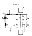
- FIG. 2 shows two further secondary circuits A2a and A3a for a converter circuit according to FIG. 1, each of which has a transducer 12a instead of transistor 12 as a controlled switch.
- the transducer 12a is controlled by the controller 21 with a direct current. This current controls the voltage time area after which the voltage at the transducer collapses, so that the transducer practically switches through. Since the controller 21 forms the control current as an analog variable as a function of the control deviation, the clock generator 19 and the pulse width modulator 20 according to FIG. 1 are not required, so that the control effort is particularly low.
- Another advantage is that the two secondary windings 3da and 3ea do not need to be galvanically separated from one another, since the two regulators control the associated transducers with a direct current.
- connection point between the secondary windings 3da and 3da is led directly to a connection a, which is common to the two outputs, at which the output voltages U22a and U23a are available. With respect to the connection a, the output voltages U22a and U23a are directed in opposite directions.
Landscapes
- Engineering & Computer Science (AREA)
- Power Engineering (AREA)
- Dc-Dc Converters (AREA)
- Input Circuits Of Receivers And Coupling Of Receivers And Audio Equipment (AREA)
- Transmitters (AREA)
Priority Applications (1)
| Application Number | Priority Date | Filing Date | Title |
|---|---|---|---|
| AT88103635T ATE77018T1 (de) | 1987-03-27 | 1988-03-08 | Umrichterschaltung mit einem eintaktsperrumrichter. |
Applications Claiming Priority (2)
| Application Number | Priority Date | Filing Date | Title |
|---|---|---|---|
| DE3710181 | 1987-03-27 | ||
| DE3710181 | 1987-03-27 |
Publications (2)
| Publication Number | Publication Date |
|---|---|
| EP0283842A1 true EP0283842A1 (fr) | 1988-09-28 |
| EP0283842B1 EP0283842B1 (fr) | 1992-06-03 |
Family
ID=6324161
Family Applications (1)
| Application Number | Title | Priority Date | Filing Date |
|---|---|---|---|
| EP88103635A Expired - Lifetime EP0283842B1 (fr) | 1987-03-27 | 1988-03-08 | Convertisseur à découpage et récupération |
Country Status (6)
| Country | Link |
|---|---|
| US (1) | US4833582A (fr) |
| EP (1) | EP0283842B1 (fr) |
| JP (1) | JPS63257458A (fr) |
| AT (1) | ATE77018T1 (fr) |
| AU (1) | AU602070B2 (fr) |
| DE (1) | DE3871577D1 (fr) |
Cited By (7)
| Publication number | Priority date | Publication date | Assignee | Title |
|---|---|---|---|---|
| DE3837933A1 (de) * | 1988-11-09 | 1990-05-10 | Philips Patentverwaltung | Getaktete stromversorgungseinrichtung |
| DE3918134A1 (de) * | 1989-06-03 | 1990-12-06 | Philips Patentverwaltung | Getaktete stromversorgungseinrichtung |
| DE4219354A1 (de) * | 1992-06-12 | 1993-12-16 | Frako Kondensator Apparate | Schaltungsanordnung zur Spannungsstabilisierung durch Impulsbreitenmodulation einer Zusatz-Ausgangsschaltung an einem Schaltnetzteil |
| EP0709949A3 (fr) * | 1994-10-24 | 1996-07-17 | Telefonica Nacional Espana Co | Convertisseur continu-continu pour alimentation |
| AT404306B (de) * | 1994-08-22 | 1998-10-27 | Siemens Ag Oesterreich | Sperrwandlerschaltung |
| DE10207752A1 (de) * | 2002-02-23 | 2003-09-04 | Thomson Brandt Gmbh | Stromversorgung mit einem Schaltnetzteil |
| DE10221710A1 (de) * | 2002-05-16 | 2003-11-27 | Thomson Brandt Gmbh | Stromversorgung mit einem Schaltnetzteil |
Families Citing this family (16)
| Publication number | Priority date | Publication date | Assignee | Title |
|---|---|---|---|---|
| US4945465A (en) * | 1988-09-15 | 1990-07-31 | U.S. Philips Corporation | Switched-mode power supply circuit |
| JPH0652970B2 (ja) * | 1989-03-29 | 1994-07-06 | 日本電気株式会社 | 電源システム |
| JP2559682Y2 (ja) * | 1990-10-17 | 1998-01-19 | 富士電機 株式会社 | 多出力スイッチングレギュレータ |
| US5122945A (en) * | 1991-04-30 | 1992-06-16 | Reliance Comm/Tec Corporation | Voltage controlled preload |
| US5619403A (en) * | 1992-07-24 | 1997-04-08 | Canon Kabushiki Kaisha | Multi-output power supply apparatus |
| JPH07135771A (ja) * | 1993-11-09 | 1995-05-23 | Hitachi Ltd | 2出力dc−dcコンバータ |
| KR0153863B1 (ko) * | 1995-12-28 | 1998-12-15 | 김광호 | 멀티 출력 스위칭 레귤레이터 |
| DE19609123C2 (de) * | 1996-03-08 | 1998-01-29 | Siemens Ag | Schaltungsanordnung für Schaltnetzteile mit mehreren lastunabhängigen Ausgangsspannungen |
| US5999417A (en) | 1997-01-24 | 1999-12-07 | Fische, Llc | High efficiency power converter |
| US7269034B2 (en) | 1997-01-24 | 2007-09-11 | Synqor, Inc. | High efficiency power converter |
| US6081437A (en) * | 1998-12-03 | 2000-06-27 | Shin Jiuh Corp. | Load balancer for a power supplying system |
| US6552917B1 (en) * | 2001-11-05 | 2003-04-22 | Koninklijke Philips Electronics N.V. | System and method for regulating multiple outputs in a DC-DC converter |
| US6775155B2 (en) * | 2002-11-05 | 2004-08-10 | Power Integrations, Inc. | Method and apparatus for output voltage regulation in primary controlled switched mode power supplies |
| US7688045B2 (en) * | 2006-08-07 | 2010-03-30 | Addtek Corp. | DC power conversion circuit with constant current output |
| JP4925316B2 (ja) * | 2007-06-14 | 2012-04-25 | パナソニック株式会社 | 電源装置 |
| US10199950B1 (en) | 2013-07-02 | 2019-02-05 | Vlt, Inc. | Power distribution architecture with series-connected bus converter |
Citations (2)
| Publication number | Priority date | Publication date | Assignee | Title |
|---|---|---|---|---|
| FR2443763A1 (fr) * | 1978-12-08 | 1980-07-04 | Philips Nv | Alimentation a decoupage comportant plusieurs sorties |
| EP0178343A1 (fr) * | 1984-10-18 | 1986-04-23 | HONEYWELL BULL ITALIA S.p.A. | Alimentation de puissance à découpage avec plusieurs sorties |
Family Cites Families (9)
| Publication number | Priority date | Publication date | Assignee | Title |
|---|---|---|---|---|
| JPS52111647A (en) * | 1976-03-15 | 1977-09-19 | Matsushita Electric Ind Co Ltd | Multioutput switching regulator circuit |
| JPS5822942B2 (ja) * | 1978-04-27 | 1983-05-12 | 富士通株式会社 | 電力変換器 |
| JPS5577372A (en) * | 1978-12-01 | 1980-06-11 | Nec Corp | Multi-output converter |
| DE2930198C2 (de) * | 1979-07-25 | 1984-11-29 | Siemens AG, 1000 Berlin und 8000 München | Durchflußumrichter mit EMK-Regelung |
| JPS5686070A (en) * | 1979-12-14 | 1981-07-13 | Fujitsu Ltd | Multioutput dc-dc converter |
| JPS5992589A (ja) * | 1982-11-18 | 1984-05-28 | Nec Corp | 半導体レ−ザ装置 |
| JPS60197162A (ja) * | 1984-03-21 | 1985-10-05 | Tdk Corp | スイツチング電源 |
| GB8508064D0 (en) * | 1985-03-28 | 1985-05-01 | Coutant Electronics Ltd | Electrical power supplies |
| US4642743A (en) * | 1985-08-05 | 1987-02-10 | International Business Machines Corp. | Power supplies with magnetic amplifier voltage regulation |
-
1988
- 1988-02-29 US US07/161,759 patent/US4833582A/en not_active Expired - Fee Related
- 1988-03-08 DE DE8888103635T patent/DE3871577D1/de not_active Expired - Lifetime
- 1988-03-08 EP EP88103635A patent/EP0283842B1/fr not_active Expired - Lifetime
- 1988-03-08 AT AT88103635T patent/ATE77018T1/de not_active IP Right Cessation
- 1988-03-25 JP JP63069938A patent/JPS63257458A/ja active Pending
- 1988-03-25 AU AU13750/88A patent/AU602070B2/en not_active Ceased
Patent Citations (2)
| Publication number | Priority date | Publication date | Assignee | Title |
|---|---|---|---|---|
| FR2443763A1 (fr) * | 1978-12-08 | 1980-07-04 | Philips Nv | Alimentation a decoupage comportant plusieurs sorties |
| EP0178343A1 (fr) * | 1984-10-18 | 1986-04-23 | HONEYWELL BULL ITALIA S.p.A. | Alimentation de puissance à découpage avec plusieurs sorties |
Non-Patent Citations (1)
| Title |
|---|
| EDN MAGAZINE, Band 26, Nr. 3, Februar 1981, Seiten 95-108, Boston, Mass., US; E.R. TEJA: "The latest switchers allow you to take advantage of their low cost and small size in a wider variety of applications than ever" * |
Cited By (7)
| Publication number | Priority date | Publication date | Assignee | Title |
|---|---|---|---|---|
| DE3837933A1 (de) * | 1988-11-09 | 1990-05-10 | Philips Patentverwaltung | Getaktete stromversorgungseinrichtung |
| DE3918134A1 (de) * | 1989-06-03 | 1990-12-06 | Philips Patentverwaltung | Getaktete stromversorgungseinrichtung |
| DE4219354A1 (de) * | 1992-06-12 | 1993-12-16 | Frako Kondensator Apparate | Schaltungsanordnung zur Spannungsstabilisierung durch Impulsbreitenmodulation einer Zusatz-Ausgangsschaltung an einem Schaltnetzteil |
| AT404306B (de) * | 1994-08-22 | 1998-10-27 | Siemens Ag Oesterreich | Sperrwandlerschaltung |
| EP0709949A3 (fr) * | 1994-10-24 | 1996-07-17 | Telefonica Nacional Espana Co | Convertisseur continu-continu pour alimentation |
| DE10207752A1 (de) * | 2002-02-23 | 2003-09-04 | Thomson Brandt Gmbh | Stromversorgung mit einem Schaltnetzteil |
| DE10221710A1 (de) * | 2002-05-16 | 2003-11-27 | Thomson Brandt Gmbh | Stromversorgung mit einem Schaltnetzteil |
Also Published As
| Publication number | Publication date |
|---|---|
| JPS63257458A (ja) | 1988-10-25 |
| EP0283842B1 (fr) | 1992-06-03 |
| AU1375088A (en) | 1988-09-29 |
| DE3871577D1 (de) | 1992-07-09 |
| US4833582A (en) | 1989-05-23 |
| AU602070B2 (en) | 1990-09-27 |
| ATE77018T1 (de) | 1992-06-15 |
Similar Documents
| Publication | Publication Date | Title |
|---|---|---|
| EP0283842B1 (fr) | Convertisseur à découpage et récupération | |
| DE19545154C2 (de) | Stromversorgungseinrichtung | |
| DE69722625T2 (de) | Eintakt-durchflussumrichter für gleichstrom-gleichstrom-umwandlung mit verbesserter rücksetzung für synchrongleichrichtung | |
| EP0373670B1 (fr) | Disposition de circuit pour un onduleur ou un convertisseur de courant continu | |
| DE69302461T2 (de) | Spannungssteuerschaltungen | |
| DE10214190B4 (de) | Stromversorgung mit mehreren parallel geschalteten Schaltnetzteilen | |
| DE3011086A1 (de) | Gleichspannungswandler | |
| DE2030547A1 (de) | Gleichspannungsregler mit mehreren Ausgangen | |
| DE3242023A1 (de) | Schaltungsanordnung zur speisung von elektrischen verbrauchern mit einer gleichspannung | |
| DE3885857T2 (de) | Spannungsschaltregler für wechselstrom. | |
| EP0521901B1 (fr) | Dispositif d'alimentation ininterrompue en courant electrique | |
| DE2246505A1 (de) | Netzgespeistes gleichstromversorgungsgeraet mit vernachlaessigbarer restwelligkeit | |
| DE2949070A1 (de) | Getaktetes netzgeraet mit mehreren ausgaengen | |
| DE3036616C2 (fr) | ||
| DE3535020A1 (de) | Wechselstrom-gleichstromwandler | |
| DE3238127A1 (de) | Anordnung zur steuerung von halbleiterschaltungen | |
| EP0772284A2 (fr) | Circuit pour la génération de tensions continues de différentes valeurs | |
| EP0302433B1 (fr) | Convertisseur à récupération | |
| DE2714152A1 (de) | Schaltungsanordnung zur erzeugung von spannungen mit wechselnder polaritaet aus einer gleichspannung | |
| DE1948257C3 (de) | Verfahren und Anordnung zur Erzeugung eines Zündimpulses mit einer hohen steilen Spitze und einem Impulsrücken | |
| DE3509853C2 (fr) | ||
| DE2035177C3 (de) | Gleichspannungsregelschaltung | |
| DE3942427A1 (de) | Schaltungsanordnung zum aufbau unterbrechungsfreier stromversorgungseinheiten | |
| EP0071878A2 (fr) | Dispositif d'alimentation en courant | |
| DE102015113071B4 (de) | Potentialverschiebende Halbbrücke, Polwender und blindleistungsfähiger Wechselrichter sowie Polwendeverfahren |
Legal Events
| Date | Code | Title | Description |
|---|---|---|---|
| PUAI | Public reference made under article 153(3) epc to a published international application that has entered the european phase |
Free format text: ORIGINAL CODE: 0009012 |
|
| AK | Designated contracting states |
Kind code of ref document: A1 Designated state(s): AT CH DE FR GB IT LI NL |
|
| 17P | Request for examination filed |
Effective date: 19890126 |
|
| 17Q | First examination report despatched |
Effective date: 19910111 |
|
| GRAA | (expected) grant |
Free format text: ORIGINAL CODE: 0009210 |
|
| AK | Designated contracting states |
Kind code of ref document: B1 Designated state(s): AT CH DE FR GB IT LI NL |
|
| PG25 | Lapsed in a contracting state [announced via postgrant information from national office to epo] |
Ref country code: IT Free format text: LAPSE BECAUSE OF FAILURE TO SUBMIT A TRANSLATION OF THE DESCRIPTION OR TO PAY THE FEE WITHIN THE PRE;WARNING: LAPSES OF ITALIAN PATENTS WITH EFFECTIVE DATE BEFORE 2007 MAY HAVE OCCURRED AT ANY TIME BEFORE 2007. THE CORRECT EFFECTIVE DATE MAY BE DIFFERENT FROM THE ONE RECORDED.SCRIBED TIME-LIMIT Effective date: 19920603 Ref country code: FR Effective date: 19920603 Ref country code: GB Effective date: 19920603 Ref country code: NL Effective date: 19920603 |
|
| REF | Corresponds to: |
Ref document number: 77018 Country of ref document: AT Date of ref document: 19920615 Kind code of ref document: T |
|
| REF | Corresponds to: |
Ref document number: 3871577 Country of ref document: DE Date of ref document: 19920709 |
|
| EN | Fr: translation not filed | ||
| NLV1 | Nl: lapsed or annulled due to failure to fulfill the requirements of art. 29p and 29m of the patents act | ||
| GBV | Gb: ep patent (uk) treated as always having been void in accordance with gb section 77(7)/1977 [no translation filed] | ||
| PGFP | Annual fee paid to national office [announced via postgrant information from national office to epo] |
Ref country code: AT Payment date: 19930224 Year of fee payment: 6 |
|
| PLBI | Opposition filed |
Free format text: ORIGINAL CODE: 0009260 |
|
| PG25 | Lapsed in a contracting state [announced via postgrant information from national office to epo] |
Ref country code: LI Free format text: LAPSE BECAUSE OF NON-PAYMENT OF DUE FEES Effective date: 19930331 Ref country code: CH Free format text: LAPSE BECAUSE OF NON-PAYMENT OF DUE FEES Effective date: 19930331 |
|
| 26 | Opposition filed |
Opponent name: PHILIPS PATENTVERWALTUNG GMBH Effective date: 19930226 |
|
| REG | Reference to a national code |
Ref country code: CH Ref legal event code: PL |
|
| PG25 | Lapsed in a contracting state [announced via postgrant information from national office to epo] |
Ref country code: DE Effective date: 19931201 |
|
| RDAG | Patent revoked |
Free format text: ORIGINAL CODE: 0009271 |
|
| STAA | Information on the status of an ep patent application or granted ep patent |
Free format text: STATUS: PATENT REVOKED |
|
| 27W | Patent revoked |
Effective date: 19931217 |