EP0283952A2 - Commande pour onduleur à modulation de largeur d'impulsion - Google Patents
Commande pour onduleur à modulation de largeur d'impulsion Download PDFInfo
- Publication number
- EP0283952A2 EP0283952A2 EP88104351A EP88104351A EP0283952A2 EP 0283952 A2 EP0283952 A2 EP 0283952A2 EP 88104351 A EP88104351 A EP 88104351A EP 88104351 A EP88104351 A EP 88104351A EP 0283952 A2 EP0283952 A2 EP 0283952A2
- Authority
- EP
- European Patent Office
- Prior art keywords
- output
- frequency
- signal generator
- signal
- generator
- Prior art date
- Legal status (The legal status is an assumption and is not a legal conclusion. Google has not performed a legal analysis and makes no representation as to the accuracy of the status listed.)
- Granted
Links
Images


Classifications
-
- H—ELECTRICITY
- H02—GENERATION; CONVERSION OR DISTRIBUTION OF ELECTRIC POWER
- H02P—CONTROL OR REGULATION OF ELECTRIC MOTORS, ELECTRIC GENERATORS OR DYNAMO-ELECTRIC CONVERTERS; CONTROLLING TRANSFORMERS, REACTORS OR CHOKE COILS
- H02P27/00—Arrangements or methods for the control of AC motors characterised by the kind of supply voltage
- H02P27/04—Arrangements or methods for the control of AC motors characterised by the kind of supply voltage using variable-frequency supply voltage, e.g. inverter or converter supply voltage
- H02P27/06—Arrangements or methods for the control of AC motors characterised by the kind of supply voltage using variable-frequency supply voltage, e.g. inverter or converter supply voltage using DC to AC converters or inverters
- H02P27/08—Arrangements or methods for the control of AC motors characterised by the kind of supply voltage using variable-frequency supply voltage, e.g. inverter or converter supply voltage using DC to AC converters or inverters with pulse width modulation
-
- G—PHYSICS
- G06—COMPUTING OR CALCULATING; COUNTING
- G06F—ELECTRIC DIGITAL DATA PROCESSING
- G06F1/00—Details not covered by groups G06F3/00 - G06F13/00 and G06F21/00
- G06F1/02—Digital function generators
- G06F1/03—Digital function generators working, at least partly, by table look-up
- G06F1/0321—Waveform generators, i.e. devices for generating periodical functions of time, e.g. direct digital synthesizers
- G06F1/0328—Waveform generators, i.e. devices for generating periodical functions of time, e.g. direct digital synthesizers in which the phase increment is adjustable, e.g. by using an adder-accumulator
- G06F1/0335—Waveform generators, i.e. devices for generating periodical functions of time, e.g. direct digital synthesizers in which the phase increment is adjustable, e.g. by using an adder-accumulator the phase increment itself being a composed function of two or more variables, e.g. frequency and phase
-
- H—ELECTRICITY
- H02—GENERATION; CONVERSION OR DISTRIBUTION OF ELECTRIC POWER
- H02M—APPARATUS FOR CONVERSION BETWEEN AC AND AC, BETWEEN AC AND DC, OR BETWEEN DC AND DC, AND FOR USE WITH MAINS OR SIMILAR POWER SUPPLY SYSTEMS; CONVERSION OF DC OR AC INPUT POWER INTO SURGE OUTPUT POWER; CONTROL OR REGULATION THEREOF
- H02M7/00—Conversion of AC power input into DC power output; Conversion of DC power input into AC power output
- H02M7/42—Conversion of DC power input into AC power output without possibility of reversal
- H02M7/44—Conversion of DC power input into AC power output without possibility of reversal by static converters
- H02M7/48—Conversion of DC power input into AC power output without possibility of reversal by static converters using discharge tubes with control electrode or semiconductor devices with control electrode
- H02M7/505—Conversion of DC power input into AC power output without possibility of reversal by static converters using discharge tubes with control electrode or semiconductor devices with control electrode using devices of a thyratron or thyristor type requiring extinguishing means
- H02M7/515—Conversion of DC power input into AC power output without possibility of reversal by static converters using discharge tubes with control electrode or semiconductor devices with control electrode using devices of a thyratron or thyristor type requiring extinguishing means using semiconductor devices only
- H02M7/525—Conversion of DC power input into AC power output without possibility of reversal by static converters using discharge tubes with control electrode or semiconductor devices with control electrode using devices of a thyratron or thyristor type requiring extinguishing means using semiconductor devices only with automatic control of output waveform or frequency
- H02M7/527—Conversion of DC power input into AC power output without possibility of reversal by static converters using discharge tubes with control electrode or semiconductor devices with control electrode using devices of a thyratron or thyristor type requiring extinguishing means using semiconductor devices only with automatic control of output waveform or frequency by pulse width modulation
- H02M7/529—Conversion of DC power input into AC power output without possibility of reversal by static converters using discharge tubes with control electrode or semiconductor devices with control electrode using devices of a thyratron or thyristor type requiring extinguishing means using semiconductor devices only with automatic control of output waveform or frequency by pulse width modulation using digital control
-
- G—PHYSICS
- G06—COMPUTING OR CALCULATING; COUNTING
- G06F—ELECTRIC DIGITAL DATA PROCESSING
- G06F2101/00—Indexing scheme relating to the type of digital function generated
- G06F2101/04—Trigonometric functions
Definitions
- the present invention relates to an apparatus for controlling a pulse width-modulated (hereinafter referred to as PWM) inverter which converts a DC power into an AC power. More specifically, the invention relates to a PWM inverter which, in an asynchronous operation mode of a low output frequency, performs asynchronous operation with a constant cut period irrespective of the change in the output frequency and which, in a synchronous operation of a high output frequency, performs synchronous operation whose cut period changes accompanying the change in the output frequency.
- PWM pulse width-modulated
- both the synchronous carrier waves and the asynchronous carrier waves must be produced at the same time, requiring a complex circuit structure.
- the present invention was accomplished to improve the above-mentioned defects, and its object is to provide a PWM inverter which is capable of being smoothly shifted from the asynchronous operation to the synchronous operation without simultaneously producing the asynchronous carrier waves and the synchronous carrier waves.
- the above object is accomplished by the provision of a frequency commander, a first digital signal generator, a timing signal generator, and adder, a phase detector, a selector, a second digital signal generator, a sinusoidal data selector, a digital calculator, a PWM signal generator, and a drive circuit.
- the frequency commander commands a frequency that is to be produced by the inverter.
- the first digital signal generator receives an output of the frequency commander, and produces a digital signal of a level that corresponds to the output in an asynchronous operation mode where the output is small, and produces a digital signal of a predetermined level in a range of low output frequencies in a synchronous operation mode where the output is great.
- the timing signal generator generates pulses of a predetermined period in the asynchronous operation mode, and generates pulse signals of a period that corresponds to the output of the frequency commander in at least a range of low output frequencies in the synchronous operation mode.
- the adder produces a phase signal by adding up signals produced by the first digital signal generator every time when the timing signal generator produces a signal, and produces a value obtained by subtracting 2 ⁇ from the added value when the phase signal has exceeded 2 ⁇ .
- the phase detector detects an output of the adder that lies within a predetermined range.
- the selector switches the asynchronous operation to the synchronous operation when the output of the frequency commander becomes greater than a predetermined value and the output of the phase detector lies within a predetermined range of output of the adder.
- the second digital signal generator works in response to the output of the frequency commander and produces a digital signal whose level increases with the increase in the level of the above output.
- the sinusoidal waveform generator receives the output of the adder, and produces data of a sinusoidal waveform that corresponds to the phase signal produced by the adder.
- the digital calculator receives output of the second digital signal generator and output of the sinusoidal wave generator in synchronism with a timing signal produced by the timing signal generator, and calculates a timing for generating a PWM signal.
- the PWM signal generator generates a PWM signal based upon the output of the digital calculator.
- the drive circuit produces a drive signal that will be fed to a power element of the inverter in response to the output of the PWM signal generator.
- the drive circuit has been disclosed in detail in USP 4,615,000.
- Equations equivalent to the equations (1) and (1 ⁇ ) have been disclosed in USP 4,615,000.
- the period of output pulses of the timing signal generator is related to the period of the carrier wave, and the output of the timing signal generator is in synchronism with the carrier waves (i.e., imaginary carrier waves since they are not really produced).
- the output of the adder represents the phase of the modulated waves (i.e., imaginary modulated waves since they are not really produced).
- the operation can be shifted from the asynchronous operation to the synchronous operation involving little transient phenomenon without the need of producing the asynchronous carrier waves and synchronous carrier waves simultaneously.
- the AC power supplied from a three-phase AC power source 10 is converted by a converter 11 into the DC power, smoothed by a smoothing capacitor 12, converted again by an inverter 13 into the AC power, and is supplied to an electric motor 14.
- reference numeral 20 denotes a frequency commander which consists of a frequency setter 20a and a lump circuit 20b.
- the frequency commander sets a frequency F out that is to be produced by the inverter 13.
- the lump circuit 20b produces a digital value.
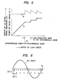
- the output D(f) of the first digital signal generator 1 exhibits characteristics as represented by a line (a) in Fig. 5 with respect to the output of the frequency commander 20.
- the abscissa represents a relationship of the asynchronous mode and the synchronous mode.
- Digital signals D(f) of a preset frequency generated by the first digital signal generator 1 are added up together by an adder 2 for each of the timing pulses Pl generated by a timing generator 4 such as a timer or the like.
- the period of output pulses generated by the timing signal generator 4 exhibits characteristics as represented by a line (b) in Fig. 5.
- the output D(f) of the first digital signal generator 1 is added up after every predetermined period. Further, the output D(f) increases with the increase in the output of the lump circuit 20b.
- the value of the output D(f) changes stepwisely, while the period ⁇ t of timing pulses P produced by the timing generator 4 changes in the form of saw tooth.
- the cut number of PWM in one period changes in the output of the inverter 13. The cut number stepwisely decreases with the increase in the output of the frequency commander 20.
- a sinusoidal wave generator 3 generates data of a sinusoidal wave sin ⁇ depending upon the added result ⁇ of the adder 2 . That is, the added result ⁇ of the adder 2 assumes a phase of the sinusoidal wave to obtain data of sinusoidal wave that corresponds to the phase. As the phase is exceeded by 360° of sinusoidal waves, the adder holds an initial value obtained by subtracting 360° therefrom.
- the second digital signal generator produces digital data of an output voltage command of a magnitude that corresponds to the output of the frequency commander 20.
- the output voltage command corresponds to the preset frequency as shown in Fig. 4. The greater the output voltage command, the greater the output. For example, by obtaining data on given characteristics among the characteristics lines c, d, e and g of Fig. 4, there can be expressed any voltage and frequency characteristics.
- the second digital signal generator 5 can be realized using a memory element such as a memory device.
- the digital calculator 6 Upon receipt of each timing pulse generated from the timing generator 4, the digital calculator 6 calculates the aforementioned equations (1) and (1 ⁇ ) relying upon the sinusoidal wave digital data produced from the sinusoidal wave generator 3 and the output voltage command (digital) produced from the second digital signal generator 5.
- the timings generated by the PWM signals are calculated, i.e., the times Tp1 and Tp2 are calculated from the vertex of the carrier wave of Fig. 3 to the rise and break of the PWM signals.
- the PWM signal generator 7 Utilizing the result of this calculation, the PWM signal generator 7 generates PWM signal.
- the PWM signals are amplified through a drive circuit a and are supplied to a power element of the inverter 13.
- the timing pulses produced from the timing signal generator 4 represent vertexes P, P ⁇ of the carrier wave of Fig. 3. In the case of the asynchronous operation mode, the timing becomes constant as shown in Fig. 5. Further, the sinusoidal wave data produced from the sinusoidal generator 3 form modulated waves in Fig. 3, and the output of the adder 2 forms a phase ⁇ of the modulated wave.
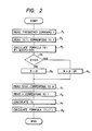
- Fig. 2 is a flow chart for synthesizing the PWM waveform.
- a frequency command f is read from the frequency commander 20.
- the first digital signal generator 1 produces D(f) that corresponds to the frequency command f.
- the adder 2 discriminate ⁇ >2 ⁇ in a process block P4.
- ⁇ ⁇ is produced.
- the process blocks P5 and P6 are executed by the adder 2.
- the sinusoidal wave data generator 3 produces sin ⁇ that corresponds to ⁇ , and the digital calculator 6 receives it.
- the second digital signal generator 5 produces a voltage command V that corresponds to the frequency command f, and the digital calculator 6 receives it.
- the digital calculator 6 finds TC from the timing signal Pl received in the previous time and the timing signal Pl received this time.
- the digital calculator 6 executes the equations (1) and (1 ⁇ ) relying upon sin ⁇ 1, V and Tc that are received in the process blocks P7, P8 and P9.
- Flow of the aforementioned control operation is interrupted by a timing pulse Pl generated from the timing signal generator 4, and is repeated every after the interrupt. If the interrupt is constant, the carrier wave frequency remains constant, and change in the output frequency is determined by the addition of phases, i.e., determined by the digital data D(f) of a present frequency.
- phase detector 21 does not produce signal h. If the result ⁇ is greater than ⁇ , i.e., greater than the predetermined range, the phase detector 21 does not produce signal h. If the result ⁇ is smaller than ⁇ , i.e., lies within the predetermined range, the phase detector 21 produces a signal h.
- D(f)/2 - 360° remains constant during the asynchronous operation mode.
- the comparator circuit 23 compares the output of the frequency commander 20 with a select frequency command fc, and produces a signal i when the output of the frequency commander 20 is equal to, or greater than, the select frequency command fc.
- the AND circuit 24 produces a signal j when there holds an AND condition of the signals h and i. Unless the signal j is produced, the timing signal generator 4 and the first digital signal generator 1 produce signals of under the asynchronous mode shown in Fig. 5 despite the frequency commander 20 is producing a command of a level large enough to shift the operation to the synchronous operation.
- the first digital signal generator 1 produces a signal that increases with the increase in the output of the frequency commander 20 and the timing signal generator 4 produces timing pulses of a predetermined period.
- the signal j is produced, a signal is produced as shown in the synchronous mode of Fig. 5. Therefore, the inverter is shifted from the asynchronous operation to the synchronous operation.
- the phase detector may be so designed as to receive the output sin ⁇ of the sinusoidal waveform generator as indicated by a dotted line in Fig. 1 and to produce the signal h by determining whether the absolute value of the output sin ⁇ lies within a predetermined range at a zero-cross point.
Landscapes
- Engineering & Computer Science (AREA)
- Power Engineering (AREA)
- Theoretical Computer Science (AREA)
- Physics & Mathematics (AREA)
- General Engineering & Computer Science (AREA)
- General Physics & Mathematics (AREA)
- Inverter Devices (AREA)
Applications Claiming Priority (2)
| Application Number | Priority Date | Filing Date | Title |
|---|---|---|---|
| JP62063917A JPH0779551B2 (ja) | 1987-03-20 | 1987-03-20 | インバ−タ制御装置 |
| JP63917/87 | 1987-03-20 |
Publications (3)
| Publication Number | Publication Date |
|---|---|
| EP0283952A2 true EP0283952A2 (fr) | 1988-09-28 |
| EP0283952A3 EP0283952A3 (en) | 1990-05-02 |
| EP0283952B1 EP0283952B1 (fr) | 1993-07-21 |
Family
ID=13243173
Family Applications (1)
| Application Number | Title | Priority Date | Filing Date |
|---|---|---|---|
| EP88104351A Expired - Lifetime EP0283952B1 (fr) | 1987-03-20 | 1988-03-18 | Commande pour onduleur à modulation de largeur d'impulsion |
Country Status (4)
| Country | Link |
|---|---|
| US (1) | US4802077A (fr) |
| EP (1) | EP0283952B1 (fr) |
| JP (1) | JPH0779551B2 (fr) |
| DE (1) | DE3882401T2 (fr) |
Cited By (4)
| Publication number | Priority date | Publication date | Assignee | Title |
|---|---|---|---|---|
| EP0467374A3 (en) * | 1990-07-20 | 1992-04-15 | Fuji Electric Co., Ltd. | Control circuit for an invertor operable in an individual mode and an interconnection mode |
| FR2738689A1 (fr) * | 1995-08-16 | 1997-03-14 | Telefunken Microelectron | Procede pour reduire la creation d'harmoniques dans le reseau d'alimentation par la commande de machines electriques |
| EP0798856A1 (fr) * | 1996-03-29 | 1997-10-01 | STMicroelectronics S.A. | Circuit de production d'impulsions |
| CN109714004A (zh) * | 2018-09-19 | 2019-05-03 | 西安石油大学 | 一种激励脉冲信号的调制方法及调制系统 |
Families Citing this family (18)
| Publication number | Priority date | Publication date | Assignee | Title |
|---|---|---|---|---|
| US5123080A (en) * | 1987-03-20 | 1992-06-16 | Ranco Incorporated Of Delaware | Compressor drive system |
| JPH0681513B2 (ja) * | 1987-11-12 | 1994-10-12 | 株式会社東芝 | Pwm制御装置 |
| US5241257A (en) * | 1989-04-17 | 1993-08-31 | Emerson Electric Co. | Drive system for household appliances |
| JPH03256533A (ja) * | 1990-03-02 | 1991-11-15 | Shikoku Sogo Kenkyusho:Kk | 系統連系システム |
| US5126642A (en) * | 1991-01-31 | 1992-06-30 | Ranco Incorporated Of Delaware | Variable speed motor control |
| DE4111226A1 (de) * | 1991-04-08 | 1992-10-15 | Asea Brown Boveri | Verfahren zur steuerung elektrischer ventile eines stromrichters |
| US5481451A (en) * | 1992-10-30 | 1996-01-02 | Arex Electronics Corporation | AC-to-AC power inverter apparatus functioning without smoothing capacitor, and control method thereof |
| US5317248A (en) * | 1992-11-12 | 1994-05-31 | General Motors Corporation | Micro-controller based PWM waveform generation for a multiple phase AC machine |
| US5841313A (en) * | 1995-08-30 | 1998-11-24 | Cherry Semiconductor Corporation | Switch with programmable delay |
| US5777443A (en) * | 1996-01-30 | 1998-07-07 | R.R. Donnelley & Sons Company | Segmented drive system for a binding line |
| US5835363A (en) * | 1997-11-13 | 1998-11-10 | Acer Peripherals, Inc. | Power supply device featuring synchronous mode and asynchronous mode operation |
| JP2004274975A (ja) * | 2003-03-12 | 2004-09-30 | Calsonic Kansei Corp | Pwm駆動装置 |
| TWI226148B (en) * | 2003-07-04 | 2005-01-01 | Delta Electronics Inc | Phase and pulse width modulation fan speed control circuit |
| TWI322561B (en) * | 2003-11-19 | 2010-03-21 | Delta Electronics Inc | Motor control circuit |
| US7049771B2 (en) * | 2004-01-27 | 2006-05-23 | Nippon Yusoki Co., Ltd. | Multi-phase carrier signal generator and multi-phase carrier signal generation method |
| US7049778B2 (en) * | 2004-02-09 | 2006-05-23 | Nippon Yusoki Co., Ltd. | Inverter control apparatus and inverter control method |
| KR101300380B1 (ko) * | 2012-03-02 | 2013-08-29 | 엘에스산전 주식회사 | 인버터 제어방법 |
| US9998054B1 (en) * | 2016-04-21 | 2018-06-12 | Summit Esp, Llc | Electric submersible pump variable speed drive controller |
Family Cites Families (3)
| Publication number | Priority date | Publication date | Assignee | Title |
|---|---|---|---|---|
| SE415945B (sv) * | 1979-02-05 | 1980-11-10 | Asea Ab | Vexelriktare med styrbar utspenning |
| JPH07108095B2 (ja) * | 1984-01-20 | 1995-11-15 | 株式会社日立製作所 | インバータ装置及びその制御方法 |
| US4740738A (en) * | 1986-09-17 | 1988-04-26 | Westinghouse Electric Corp. | Reluctance motor control system and method |
-
1987
- 1987-03-20 JP JP62063917A patent/JPH0779551B2/ja not_active Expired - Lifetime
-
1988
- 1988-02-29 US US07/162,082 patent/US4802077A/en not_active Expired - Lifetime
- 1988-03-18 EP EP88104351A patent/EP0283952B1/fr not_active Expired - Lifetime
- 1988-03-18 DE DE88104351T patent/DE3882401T2/de not_active Expired - Lifetime
Cited By (8)
| Publication number | Priority date | Publication date | Assignee | Title |
|---|---|---|---|---|
| EP0467374A3 (en) * | 1990-07-20 | 1992-04-15 | Fuji Electric Co., Ltd. | Control circuit for an invertor operable in an individual mode and an interconnection mode |
| US5255176A (en) * | 1990-07-20 | 1993-10-19 | Fuji Electronic Co., Ltd. | Control circuit for an inverter operable in an individual mode and an interconnection mode |
| FR2738689A1 (fr) * | 1995-08-16 | 1997-03-14 | Telefunken Microelectron | Procede pour reduire la creation d'harmoniques dans le reseau d'alimentation par la commande de machines electriques |
| EP0798856A1 (fr) * | 1996-03-29 | 1997-10-01 | STMicroelectronics S.A. | Circuit de production d'impulsions |
| FR2746986A1 (fr) * | 1996-03-29 | 1997-10-03 | Sgs Thomson Microelectronics | Circuit de production d'impulsions |
| US5886555A (en) * | 1996-03-29 | 1999-03-23 | Sgs-Thomson Microelectronics S.A. | Pulse production circuit |
| CN109714004A (zh) * | 2018-09-19 | 2019-05-03 | 西安石油大学 | 一种激励脉冲信号的调制方法及调制系统 |
| CN109714004B (zh) * | 2018-09-19 | 2023-03-24 | 西安石油大学 | 一种激励脉冲信号的调制方法及调制系统 |
Also Published As
| Publication number | Publication date |
|---|---|
| DE3882401T2 (de) | 1994-01-05 |
| JPH0779551B2 (ja) | 1995-08-23 |
| DE3882401D1 (de) | 1993-08-26 |
| EP0283952A3 (en) | 1990-05-02 |
| US4802077A (en) | 1989-01-31 |
| EP0283952B1 (fr) | 1993-07-21 |
| JPS63234877A (ja) | 1988-09-30 |
Similar Documents
| Publication | Publication Date | Title |
|---|---|---|
| EP0283952A2 (fr) | Commande pour onduleur à modulation de largeur d'impulsion | |
| US6134127A (en) | PWM harmonic control | |
| EP0358225B1 (fr) | Dispositif de conversion de puissance avec suppression de battement | |
| EP0479136A1 (fr) | Commande numérique pour servo | |
| EP0254290B1 (fr) | Procédé et dispositif de commande d'un onduleur à modulation de largeur d'impulsion | |
| US5214367A (en) | Controller for compressor driven by induction motor | |
| US5121043A (en) | PWM control in the pulse dropping region | |
| JPH09149660A (ja) | Pwm制御インバータの制御装置 | |
| US4924168A (en) | Control apparatus for PWM-controlled, variable voltage/variable frequency inverters | |
| EP0732798A1 (fr) | Appareil de contrÔle à modulation de largeur d'impulsions et système utilisant celui-ci | |
| EP0467694B1 (fr) | Dispositif générateur des signaux PWM à trois phases pour onduleurs | |
| JPS61128788A (ja) | 同期電動機の制御方法 | |
| EP0160310B1 (fr) | Inverseur à commutation par la charge pour l'opération d'un moteur synchrone | |
| EP0144161B1 (fr) | Système de contrôle pour moteur à courant alternatif | |
| US4282570A (en) | Method and apparatus for controlling an output current of a controlled rectifier | |
| EP0293844B1 (fr) | Dispositif de commande pour onduleurs à tension variable/fréquence variable à modulation d'impulsion | |
| JP3391180B2 (ja) | インバータ装置 | |
| JPH02168895A (ja) | 電圧形パルス幅変調制御インバータの電流ピーク値低減方法 | |
| JP2607488B2 (ja) | インバータ制御装置 | |
| KR900002421B1 (ko) | 인버어터 구동제어장치 | |
| JPH07245876A (ja) | 系統連系インバータの制御装置 | |
| JP3396775B2 (ja) | 逆変換器の制御回路 | |
| JPH0734680B2 (ja) | 誘導電動機のベクトル制御方法及び装置 | |
| JPH0158759B2 (fr) | ||
| JPH0239195B2 (fr) |
Legal Events
| Date | Code | Title | Description |
|---|---|---|---|
| PUAI | Public reference made under article 153(3) epc to a published international application that has entered the european phase |
Free format text: ORIGINAL CODE: 0009012 |
|
| AK | Designated contracting states |
Kind code of ref document: A2 Designated state(s): DE FR GB IT |
|
| PUAL | Search report despatched |
Free format text: ORIGINAL CODE: 0009013 |
|
| AK | Designated contracting states |
Kind code of ref document: A3 Designated state(s): DE FR GB IT |
|
| 17P | Request for examination filed |
Effective date: 19900504 |
|
| 17Q | First examination report despatched |
Effective date: 19920327 |
|
| GRAA | (expected) grant |
Free format text: ORIGINAL CODE: 0009210 |
|
| AK | Designated contracting states |
Kind code of ref document: B1 Designated state(s): DE FR GB IT |
|
| REF | Corresponds to: |
Ref document number: 3882401 Country of ref document: DE Date of ref document: 19930826 |
|
| ET | Fr: translation filed | ||
| ITF | It: translation for a ep patent filed | ||
| PLBE | No opposition filed within time limit |
Free format text: ORIGINAL CODE: 0009261 |
|
| STAA | Information on the status of an ep patent application or granted ep patent |
Free format text: STATUS: NO OPPOSITION FILED WITHIN TIME LIMIT |
|
| 26N | No opposition filed | ||
| PGFP | Annual fee paid to national office [announced via postgrant information from national office to epo] |
Ref country code: FR Payment date: 19990316 Year of fee payment: 12 |
|
| PG25 | Lapsed in a contracting state [announced via postgrant information from national office to epo] |
Ref country code: FR Free format text: LAPSE BECAUSE OF NON-PAYMENT OF DUE FEES Effective date: 20001130 |
|
| REG | Reference to a national code |
Ref country code: FR Ref legal event code: ST |
|
| REG | Reference to a national code |
Ref country code: GB Ref legal event code: IF02 |
|
| PG25 | Lapsed in a contracting state [announced via postgrant information from national office to epo] |
Ref country code: IT Free format text: LAPSE BECAUSE OF NON-PAYMENT OF DUE FEES;WARNING: LAPSES OF ITALIAN PATENTS WITH EFFECTIVE DATE BEFORE 2007 MAY HAVE OCCURRED AT ANY TIME BEFORE 2007. THE CORRECT EFFECTIVE DATE MAY BE DIFFERENT FROM THE ONE RECORDED. Effective date: 20050318 |
|
| PGFP | Annual fee paid to national office [announced via postgrant information from national office to epo] |
Ref country code: GB Payment date: 20070222 Year of fee payment: 20 |
|
| PGFP | Annual fee paid to national office [announced via postgrant information from national office to epo] |
Ref country code: DE Payment date: 20070305 Year of fee payment: 20 |
|
| REG | Reference to a national code |
Ref country code: GB Ref legal event code: PE20 Expiry date: 20080317 |
|
| PG25 | Lapsed in a contracting state [announced via postgrant information from national office to epo] |
Ref country code: GB Free format text: LAPSE BECAUSE OF EXPIRATION OF PROTECTION Effective date: 20080317 |