EP0284190A2 - Chemisches Gasphasenabscheidungsverfahren zur Herstellung einer Kohlenstoffschicht - Google Patents
Chemisches Gasphasenabscheidungsverfahren zur Herstellung einer Kohlenstoffschicht Download PDFInfo
- Publication number
- EP0284190A2 EP0284190A2 EP88301364A EP88301364A EP0284190A2 EP 0284190 A2 EP0284190 A2 EP 0284190A2 EP 88301364 A EP88301364 A EP 88301364A EP 88301364 A EP88301364 A EP 88301364A EP 0284190 A2 EP0284190 A2 EP 0284190A2
- Authority
- EP
- European Patent Office
- Prior art keywords
- carbon
- compound
- reactive gas
- gaseous
- reaction chamber
- Prior art date
- Legal status (The legal status is an assumption and is not a legal conclusion. Google has not performed a legal analysis and makes no representation as to the accuracy of the status listed.)
- Granted
Links
Images



Classifications
-
- C—CHEMISTRY; METALLURGY
- C23—COATING METALLIC MATERIAL; COATING MATERIAL WITH METALLIC MATERIAL; CHEMICAL SURFACE TREATMENT; DIFFUSION TREATMENT OF METALLIC MATERIAL; COATING BY VACUUM EVAPORATION, BY SPUTTERING, BY ION IMPLANTATION OR BY CHEMICAL VAPOUR DEPOSITION, IN GENERAL; INHIBITING CORROSION OF METALLIC MATERIAL OR INCRUSTATION IN GENERAL
- C23C—COATING METALLIC MATERIAL; COATING MATERIAL WITH METALLIC MATERIAL; SURFACE TREATMENT OF METALLIC MATERIAL BY DIFFUSION INTO THE SURFACE, BY CHEMICAL CONVERSION OR SUBSTITUTION; COATING BY VACUUM EVAPORATION, BY SPUTTERING, BY ION IMPLANTATION OR BY CHEMICAL VAPOUR DEPOSITION, IN GENERAL
- C23C14/00—Coating by vacuum evaporation, by sputtering or by ion implantation of the coating forming material
- C23C14/22—Coating by vacuum evaporation, by sputtering or by ion implantation of the coating forming material characterised by the process of coating
- C23C14/24—Vacuum evaporation
-
- C—CHEMISTRY; METALLURGY
- C23—COATING METALLIC MATERIAL; COATING MATERIAL WITH METALLIC MATERIAL; CHEMICAL SURFACE TREATMENT; DIFFUSION TREATMENT OF METALLIC MATERIAL; COATING BY VACUUM EVAPORATION, BY SPUTTERING, BY ION IMPLANTATION OR BY CHEMICAL VAPOUR DEPOSITION, IN GENERAL; INHIBITING CORROSION OF METALLIC MATERIAL OR INCRUSTATION IN GENERAL
- C23C—COATING METALLIC MATERIAL; COATING MATERIAL WITH METALLIC MATERIAL; SURFACE TREATMENT OF METALLIC MATERIAL BY DIFFUSION INTO THE SURFACE, BY CHEMICAL CONVERSION OR SUBSTITUTION; COATING BY VACUUM EVAPORATION, BY SPUTTERING, BY ION IMPLANTATION OR BY CHEMICAL VAPOUR DEPOSITION, IN GENERAL
- C23C16/00—Chemical coating by decomposition of gaseous compounds, without leaving reaction products of surface material in the coating, i.e. chemical vapour deposition [CVD] processes
- C23C16/22—Chemical coating by decomposition of gaseous compounds, without leaving reaction products of surface material in the coating, i.e. chemical vapour deposition [CVD] processes characterised by the deposition of inorganic material, other than metallic material
- C23C16/26—Deposition of carbon only
- C23C16/27—Diamond only
- C23C16/274—Diamond only using microwave discharges
-
- C—CHEMISTRY; METALLURGY
- C23—COATING METALLIC MATERIAL; COATING MATERIAL WITH METALLIC MATERIAL; CHEMICAL SURFACE TREATMENT; DIFFUSION TREATMENT OF METALLIC MATERIAL; COATING BY VACUUM EVAPORATION, BY SPUTTERING, BY ION IMPLANTATION OR BY CHEMICAL VAPOUR DEPOSITION, IN GENERAL; INHIBITING CORROSION OF METALLIC MATERIAL OR INCRUSTATION IN GENERAL
- C23C—COATING METALLIC MATERIAL; COATING MATERIAL WITH METALLIC MATERIAL; SURFACE TREATMENT OF METALLIC MATERIAL BY DIFFUSION INTO THE SURFACE, BY CHEMICAL CONVERSION OR SUBSTITUTION; COATING BY VACUUM EVAPORATION, BY SPUTTERING, BY ION IMPLANTATION OR BY CHEMICAL VAPOUR DEPOSITION, IN GENERAL
- C23C16/00—Chemical coating by decomposition of gaseous compounds, without leaving reaction products of surface material in the coating, i.e. chemical vapour deposition [CVD] processes
- C23C16/06—Chemical coating by decomposition of gaseous compounds, without leaving reaction products of surface material in the coating, i.e. chemical vapour deposition [CVD] processes characterised by the deposition of metallic material
-
- C—CHEMISTRY; METALLURGY
- C23—COATING METALLIC MATERIAL; COATING MATERIAL WITH METALLIC MATERIAL; CHEMICAL SURFACE TREATMENT; DIFFUSION TREATMENT OF METALLIC MATERIAL; COATING BY VACUUM EVAPORATION, BY SPUTTERING, BY ION IMPLANTATION OR BY CHEMICAL VAPOUR DEPOSITION, IN GENERAL; INHIBITING CORROSION OF METALLIC MATERIAL OR INCRUSTATION IN GENERAL
- C23C—COATING METALLIC MATERIAL; COATING MATERIAL WITH METALLIC MATERIAL; SURFACE TREATMENT OF METALLIC MATERIAL BY DIFFUSION INTO THE SURFACE, BY CHEMICAL CONVERSION OR SUBSTITUTION; COATING BY VACUUM EVAPORATION, BY SPUTTERING, BY ION IMPLANTATION OR BY CHEMICAL VAPOUR DEPOSITION, IN GENERAL
- C23C16/00—Chemical coating by decomposition of gaseous compounds, without leaving reaction products of surface material in the coating, i.e. chemical vapour deposition [CVD] processes
- C23C16/22—Chemical coating by decomposition of gaseous compounds, without leaving reaction products of surface material in the coating, i.e. chemical vapour deposition [CVD] processes characterised by the deposition of inorganic material, other than metallic material
- C23C16/26—Deposition of carbon only
- C23C16/27—Diamond only
- C23C16/278—Diamond only doping or introduction of a secondary phase in the diamond
-
- C—CHEMISTRY; METALLURGY
- C23—COATING METALLIC MATERIAL; COATING MATERIAL WITH METALLIC MATERIAL; CHEMICAL SURFACE TREATMENT; DIFFUSION TREATMENT OF METALLIC MATERIAL; COATING BY VACUUM EVAPORATION, BY SPUTTERING, BY ION IMPLANTATION OR BY CHEMICAL VAPOUR DEPOSITION, IN GENERAL; INHIBITING CORROSION OF METALLIC MATERIAL OR INCRUSTATION IN GENERAL
- C23C—COATING METALLIC MATERIAL; COATING MATERIAL WITH METALLIC MATERIAL; SURFACE TREATMENT OF METALLIC MATERIAL BY DIFFUSION INTO THE SURFACE, BY CHEMICAL CONVERSION OR SUBSTITUTION; COATING BY VACUUM EVAPORATION, BY SPUTTERING, BY ION IMPLANTATION OR BY CHEMICAL VAPOUR DEPOSITION, IN GENERAL
- C23C16/00—Chemical coating by decomposition of gaseous compounds, without leaving reaction products of surface material in the coating, i.e. chemical vapour deposition [CVD] processes
- C23C16/44—Chemical coating by decomposition of gaseous compounds, without leaving reaction products of surface material in the coating, i.e. chemical vapour deposition [CVD] processes characterised by the method of coating
- C23C16/50—Chemical coating by decomposition of gaseous compounds, without leaving reaction products of surface material in the coating, i.e. chemical vapour deposition [CVD] processes characterised by the method of coating using electric discharges
- C23C16/511—Chemical coating by decomposition of gaseous compounds, without leaving reaction products of surface material in the coating, i.e. chemical vapour deposition [CVD] processes characterised by the method of coating using electric discharges using microwave discharges
-
- C—CHEMISTRY; METALLURGY
- C30—CRYSTAL GROWTH
- C30B—SINGLE-CRYSTAL GROWTH; UNIDIRECTIONAL SOLIDIFICATION OF EUTECTIC MATERIAL OR UNIDIRECTIONAL DEMIXING OF EUTECTOID MATERIAL; REFINING BY ZONE-MELTING OF MATERIAL; PRODUCTION OF A HOMOGENEOUS POLYCRYSTALLINE MATERIAL WITH DEFINED STRUCTURE; SINGLE CRYSTALS OR HOMOGENEOUS POLYCRYSTALLINE MATERIAL WITH DEFINED STRUCTURE; AFTER-TREATMENT OF SINGLE CRYSTALS OR A HOMOGENEOUS POLYCRYSTALLINE MATERIAL WITH DEFINED STRUCTURE; APPARATUS THEREFOR
- C30B25/00—Single-crystal growth by chemical reaction of reactive gases, e.g. chemical vapour-deposition growth
- C30B25/02—Epitaxial-layer growth
- C30B25/10—Heating of the reaction chamber or the substrate
- C30B25/105—Heating of the reaction chamber or the substrate by irradiation or electric discharge
-
- C—CHEMISTRY; METALLURGY
- C30—CRYSTAL GROWTH
- C30B—SINGLE-CRYSTAL GROWTH; UNIDIRECTIONAL SOLIDIFICATION OF EUTECTIC MATERIAL OR UNIDIRECTIONAL DEMIXING OF EUTECTOID MATERIAL; REFINING BY ZONE-MELTING OF MATERIAL; PRODUCTION OF A HOMOGENEOUS POLYCRYSTALLINE MATERIAL WITH DEFINED STRUCTURE; SINGLE CRYSTALS OR HOMOGENEOUS POLYCRYSTALLINE MATERIAL WITH DEFINED STRUCTURE; AFTER-TREATMENT OF SINGLE CRYSTALS OR A HOMOGENEOUS POLYCRYSTALLINE MATERIAL WITH DEFINED STRUCTURE; APPARATUS THEREFOR
- C30B29/00—Single crystals or homogeneous polycrystalline material with defined structure characterised by the material or by their shape
- C30B29/02—Elements
- C30B29/04—Diamond
-
- Y—GENERAL TAGGING OF NEW TECHNOLOGICAL DEVELOPMENTS; GENERAL TAGGING OF CROSS-SECTIONAL TECHNOLOGIES SPANNING OVER SEVERAL SECTIONS OF THE IPC; TECHNICAL SUBJECTS COVERED BY FORMER USPC CROSS-REFERENCE ART COLLECTIONS [XRACs] AND DIGESTS
- Y10—TECHNICAL SUBJECTS COVERED BY FORMER USPC
- Y10S—TECHNICAL SUBJECTS COVERED BY FORMER USPC CROSS-REFERENCE ART COLLECTIONS [XRACs] AND DIGESTS
- Y10S427/00—Coating processes
- Y10S427/103—Diamond-like carbon coating, i.e. DLC
-
- Y—GENERAL TAGGING OF NEW TECHNOLOGICAL DEVELOPMENTS; GENERAL TAGGING OF CROSS-SECTIONAL TECHNOLOGIES SPANNING OVER SEVERAL SECTIONS OF THE IPC; TECHNICAL SUBJECTS COVERED BY FORMER USPC CROSS-REFERENCE ART COLLECTIONS [XRACs] AND DIGESTS
- Y10—TECHNICAL SUBJECTS COVERED BY FORMER USPC
- Y10S—TECHNICAL SUBJECTS COVERED BY FORMER USPC CROSS-REFERENCE ART COLLECTIONS [XRACs] AND DIGESTS
- Y10S427/00—Coating processes
- Y10S427/103—Diamond-like carbon coating, i.e. DLC
- Y10S427/104—Utilizing low energy electromagnetic radiation, e.g. microwave, radio wave, IR, UV, visible, actinic laser
-
- Y—GENERAL TAGGING OF NEW TECHNOLOGICAL DEVELOPMENTS; GENERAL TAGGING OF CROSS-SECTIONAL TECHNOLOGIES SPANNING OVER SEVERAL SECTIONS OF THE IPC; TECHNICAL SUBJECTS COVERED BY FORMER USPC CROSS-REFERENCE ART COLLECTIONS [XRACs] AND DIGESTS
- Y10—TECHNICAL SUBJECTS COVERED BY FORMER USPC
- Y10S—TECHNICAL SUBJECTS COVERED BY FORMER USPC CROSS-REFERENCE ART COLLECTIONS [XRACs] AND DIGESTS
- Y10S427/00—Coating processes
- Y10S427/103—Diamond-like carbon coating, i.e. DLC
- Y10S427/106—Utilizing plasma, e.g. corona, glow discharge, cold plasma
Definitions
- This invention relates to an enhanced CVD method for the production of carbon thin films.
- the pressure in the resonating space is kept at 1 ⁇ 10 ⁇ 3 to 1 ⁇ 10 ⁇ 5 Torr at which pressure electrons can be considered as independent particles and will resonate with the microwave energy in an electron cyclotron resonance wherever the magnetic field strength meets the requirements for ECR.
- the excited plasma is extracted from the resonating space by means of a divergent magnetic field, and is conducted to a deposition space which is located distant from the resonating space and in which there is disposed a substrate to be coated.
- nitrogen and/or a nitrogen compound gas is introduced into the reaction chamber.
- the added nitrogen functions to prevent lattice defects from growing by virtue of external or internal stress.
- a boron compound gas may also be introduced with the nitrogen compound gas and serves to enhance the adhesivity of the deposited carbon, boron nitride appearing to be the binder between the carbon and the underlying substrate.
- Carbon and boron nitride may advantageously be deposited on the substrate in the form of crystalline grain particles or in a layer containing nitrogen and boron at less than 10%.
- an improved CVD process which utilizes a mixed cyclotron resonance.
- sonic action of the reactive gas itself must be taken into consideration as a non-negligible perturbation besides the interaction between respective particles of the reactive gas and the magnetic and microwave energy fields, and as a result charged particles of reactive gas can be absorbed in a relatively wide resonating space.
- the pressure in the reaction chamber is elevated to 102-105 times as high as that utilized in the prior art.
- mixed resonance can be established by increasing the pressure after ECR takes place at low pressure; first a plasma gas is placed in ECR condition at 1 ⁇ 10 ⁇ 3 to 1 ⁇ 10 ⁇ 5 Torr by inputting microwave energy under the influence of a magnetic field, and then a reactive gas is inputted into the plasma gas so that the pressure is elevated to 0.1 to 300 Torr, preferably greater than 3 Torr, and the resonance is changed from ECR to MCR (Mixed Cyclotron Resonance). Carbon can be decomposed and can undergo the required reaction only at such a comparatively high pressure. In operation of the process, diamond is likely to grow selectively on convexities.
- hydrogen in a plasma state acts as an etchant to preferentially eliminate amorphous carbon thereby leaving crystalline carbon.
- the hardness of diamond formed in accordance with the present invention is 1.3 to 3.0 times as high as that of diamond which has been made by prior art vapor phase methods.
- the apparatus comprises a reaction chamber defining a plasma generating space 1 and an auxiliary space 2 which can be maintained at an appropriate negative pressure, a microwave generator 4, electromagnets 5 and 5 ⁇ in the form of Helmholtz coils surrounding the space 1, a power supply 25 for supplying the electro-magnets 5 and 5 ⁇ , and a water cooling system 18.
- a reaction chamber defining a plasma generating space 1 and an auxiliary space 2 which can be maintained at an appropriate negative pressure
- a microwave generator 4 electromagnets 5 and 5 ⁇ in the form of Helmholtz coils surrounding the space 1
- a power supply 25 for supplying the electro-magnets 5 and 5 ⁇
- a water cooling system for evacuating the reaction chamber there is provided an evacuating system comprising a turbo molecular pump 17 and a rotary pump 14 which are connected to the reaction chamber through pressure controlling valves 11, 13 and 15.
- the plasma generating space 1 has a circular cross section and, within the plasma generating space 1, there is provided a substrate holder 10 ⁇ upon which a substrate 10 may be mounted, the substrate holder 10 ⁇ being made of a material such as stainless steel or quartz which provokes minimum disturbance of the magnetic field created by the magnets 5 and 5 ⁇ .
- the substrate holder 10 ⁇ is irradiated and heated to 800-1000°C in a high temperature plasma gas atmosphere by means of infrared radiation 24 which is emitted from an IR heater 20, reflected from an IR reflection parabolic mirror 21 and focused on the back surface of the holder 10 ⁇ through a lens 22.
- Reference numeral 23 designates a power supply for the IR heater 20.
- a substrate 10 is mounted on the substrate holder 10 ⁇ , and the reaction chamber is evacuated to 1 ⁇ 10 ⁇ 6 Torr or to a higher vacuum condition. Then, hydrogen gas is introduced from a gas introducing system 6 at 30 SCCM, and microwave energy at a power level of 500 Watts and a frequency of 2.45GHz is injected from the microwave generator 4 through a microwave introduction window 15 into the plasma generating space 1 which is subjected at the same time to a magnetic field of about 2 K Gauss generated by the magnets 5 and 5 ⁇ . The hydrogen is excited into a high density plasma state in the space 1 at 1 ⁇ 10 ⁇ 4 Torr by the microwave energy. The surface of the substrate 10 is cleaned by high energy electrons and hydrogen atoms.
- a productive gas comprising a carbon compound such as C2H2, C2H4, C2H6, CH3OH, C2H5OH or CH4 for example is inputted at 30 SCCM through a gas introduction system 7.
- the productive gas is diluted with hydrogen at a sufficiently low density, e.g 0.1 to 5%.
- nitrogen or a nitrogen compound gas such as ammonia for example, is inputted to the reaction chamber from the introduction system, the proportion of the nitrogen compound gas to the carbon compound gas being 0.1%-5%.
- the pressure in the reaction chamber is then maintained at 0.1 Torr-300 Torr, preferably 3-30 Torr, e.g. 1 Torr.
- the CVD reaction which occurs results from carbon atoms being excited to a high energy condition so that the substrate 10 mounted on the holder 10 ⁇ is coated with carbon in the form of a film made of i-carbon (insulated carbon consisting of microcrystals) or diamond having a grain diameter of from 0.1 to 100 microns.
- the deposited carbon contains nitrogen at 0.01 - 1% by weight.
- a substrate 10 is mounted on the substrate holder 10 ⁇ , and the reaction chamber is evacuated to 1 ⁇ 10 ⁇ 6 Torr or to a higher vacuum condition.
- hydrogen gas is introduced from the gas introducing system 6 at 300 SCCM, and microwave energy at a power level of 1 Kilowatt and a frequency of 2.45GHz is injected from the microwave generator 4 through the microwave introduction window 15 into the plasma generating space 1 which is subjected at the same time to a magnetic field of about 2 K Gauss generated by the magnets 5 and 5 ⁇ .
- the hydrogen is excited into a high density plasma state in the space 1 by the microwave energy.
- the surface of the substrate 10 is cleaned by high energy electrons and hydrogen atoms.
- a productive gas comprising a carbon compound such as C2H2, C2H4, CH3OH, C2H5OH or CH4 for example is inputted at 3 SCCM through the gas introduction system 7.
- the productive gas is diluted with hydrogen at a sufficiently low density, e.g. 0.1 to 15%.
- the pressure in the reaction chamber is then maintained at 1 Torr-760 Torr, preferably higher than 10 Torr or 10-100 Torr, e.g. 30 Torr.
- the CVD reaction which occurs causes the substrate 10 mounted on the holder 10 ⁇ to be coated with carbon containing nitrogen and boron (or in the form of boron nitride).
- the product includes carbon and boron nitride as its main constituents, the sum of whose proportions is at least 90%.
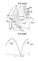
- Fig.2(A) is a graphical showing of the distribution of the magnetic field in the region 30 in Fig.1.
- the curves in the diagram are plotted along equipotential surfaces and are given numerals indicating the strengths along the respective curves of the magnetic field induced by magnets 5 and 5 ⁇ having a power of 2000 Gauss.
- the strength of the magnetic field can be controlled so that the magnetic field becomes largely uniform over the surface to be coated which is located in the region 100 where the magnetic field (875 ⁇ 185 Gauss) and the electric field interact.
- the reference 26 designates the equipotential surface of 875 Gauss at which the conditions required for ECR (electron cyclotron resonance) between the magnetic field and the microwave energy are satisfied.
- ECR electron cyclotron resonance
- MCR mixed cyclotron resonance
- Fig.2(B) is a graphical diagram in which the X-axis corresponds to that of Fig.2(A) and which shows the strength of the electric field of the microwave energy in the plasma generating space 1. As shown, the electric field strength takes its maximum value in the regions 100 and 100 ⁇ .
- a uniform film can be formed on a circular substrate having a diameter of up to 100mm, and a film can be formed in the chamber on a circular substrate having a diameter of up to 50 mm with a uniform thickness and a uniform quality.
- Figs.3(A) and 3(B) are graphical diagrams showing the distributions of the magnetic field and the electric field due to microwave energy emitted from the microwave generator 4 for a cross section of the plasma generating space 1.
- the curves in the circles of the figures are plotted along equipotential surfaces and given numerals showing the field strengths.
- the electric field reaches its maximum value at 25 KV/m.
- the film is made of a mixture of boron nitride and diamond. As the microwave power is increased from 1KW to 5KW, the proportion of diamond in the film increases.
- the plasma gas contains fluorine which functions as an etchant to eliminate impurities residing on the surface which is to be coated.
- a film formation process was performed in the same manner as in the above but without using a magnetic field. As a result, a graphite film was deposited.
- amorphous or microcrystalline film can also be deposited by appropriately selecting the deposition conditions.
- An amorphous film is deposited when the carbon compound gas is diluted with a larger amount of hydrogen gas, when the input power is comparatively small and when the process temperature is comparatively low.
- the deposited film includes a microcrystalline structure.
- the carbon formed in accordance with the invention has a very high hardness irrespective of whether the carbon is amorphous or crystalline. Its Vickers hardness is 4500-6400 Kg/mm2, e.g. 2000 Kg/mm2. The thermal conductivity is not lower than 2.5 W/cmdeg, e.g. 5.0-6.6 W/cmdeg.
- Fig.4 is a cross sectional view showing an exemplary CVD apparatus for deposition by virtue of RF energy.
- the apparatus comprises a reaction chamber 101, a loading chamber 103, a rotary pump 105 for evacuating the loading chamber 103, a turbo molecular pump 107 associated with a rotary pump 109 for evacuating both the reaction chamber 101 and the loading chamber 103, a gas feeding system 127 for inputting process gas such as reactive gas or dopant gas through a nozzle 129, a substrate holder 111 for supporting substrates 113, electrodes 115 disposed opposite to the holder 111, an RF power supply 117 consisting of a radio frequency power source 119 associated with a matching circuit 121 and a DC bias circuit 123 for supply RF energy between the electrodes 115 and the substrate holder 111, and a halogen lamp heater
- an exemplary deposition process for coating the substrates 113 with a carbon film is as follows. After disposing the substrates 113 in the reaction chamber 101 through a gate 129, a reactive gas composed of a gaseous carbon compound such as CH4, C2H4 or C2H2 for example, and a dopant gas such as nitrogen, a nitrogen compound gas and a boron compound gas if necessary were inputted to the reaction chamber at 1 ⁇ 10 ⁇ 3 to 5 ⁇ 10 ⁇ 1 Torr. The carbon compound gas was diluted with hydrogen at 50 mol%. At the same time, the substrates 113 were heated to not higher than 450°C by means of the heater 125.
- a reactive gas composed of a gaseous carbon compound such as CH4, C2H4 or C2H2 for example
- a dopant gas such as nitrogen, a nitrogen compound gas and a boron compound gas if necessary were inputted to the reaction chamber at 1 ⁇ 10 ⁇ 3 to 5 ⁇ 10 ⁇ 1 Torr.
- the carbon compound gas was
- a vapor reaction was initiated by means of RF power inputted from the power supply 117.
- the RF power was at a level of 50 W to 1 KW (0.03 to 3.00 W/cm2 and a frequency of 13.56MHz superimposed on a DC bias voltage of -200V to +400V.
- Carbon films were deposited on the substrates 113 at a growth rate of 150 ⁇ /min.
- the carbon film looked like an amorphous structure rather than a crystalline structure. Despite the amorphous structure, the hardness was measured as high as that of a diamond film.
- the Vickers hardness thereof was 4500-6400 Kg/mm2, e.g. 2000 Kg/mm2.
- a super lattice structure can be also formed.
- a boron nitride (BN) thin film may be deposited in the same way as illustrated in the above but without using carbon compound gas, and carbon thin film and a BN thin film may be deposited in turn many times so that a super lattice structure is stacked on a substrate.
- BN boron nitride
Landscapes
- Chemical & Material Sciences (AREA)
- Engineering & Computer Science (AREA)
- Metallurgy (AREA)
- Materials Engineering (AREA)
- Organic Chemistry (AREA)
- Chemical Kinetics & Catalysis (AREA)
- General Chemical & Material Sciences (AREA)
- Mechanical Engineering (AREA)
- Crystallography & Structural Chemistry (AREA)
- Inorganic Chemistry (AREA)
- Physics & Mathematics (AREA)
- Plasma & Fusion (AREA)
- Chemical Vapour Deposition (AREA)
- Crystals, And After-Treatments Of Crystals (AREA)
- Carbon And Carbon Compounds (AREA)
Applications Claiming Priority (4)
| Application Number | Priority Date | Filing Date | Title |
|---|---|---|---|
| JP41748/87 | 1987-02-24 | ||
| JP62041748A JPS63210010A (ja) | 1987-02-24 | 1987-02-24 | 炭素作製方法 |
| JP175560/87 | 1987-07-13 | ||
| JP17556087A JPH0623437B2 (ja) | 1987-07-13 | 1987-07-13 | 炭素および窒化ホウ素の作製方法 |
Publications (3)
| Publication Number | Publication Date |
|---|---|
| EP0284190A2 true EP0284190A2 (de) | 1988-09-28 |
| EP0284190A3 EP0284190A3 (en) | 1989-02-22 |
| EP0284190B1 EP0284190B1 (de) | 1992-11-25 |
Family
ID=26381396
Family Applications (1)
| Application Number | Title | Priority Date | Filing Date |
|---|---|---|---|
| EP88301364A Expired - Lifetime EP0284190B1 (de) | 1987-02-24 | 1988-02-18 | Chemisches Gasphasenabscheidungsverfahren zur Herstellung einer Kohlenstoffschicht |
Country Status (5)
| Country | Link |
|---|---|
| US (3) | US4869923A (de) |
| EP (1) | EP0284190B1 (de) |
| KR (1) | KR900008505B1 (de) |
| CN (1) | CN1036078C (de) |
| DE (1) | DE3876120T2 (de) |
Cited By (6)
| Publication number | Priority date | Publication date | Assignee | Title |
|---|---|---|---|---|
| DE3903322A1 (de) * | 1989-02-04 | 1990-08-16 | Nmi Naturwissenschaftl U Mediz | Verfahren zur erzeugung von ionen |
| FR2726579A1 (fr) * | 1994-11-07 | 1996-05-10 | Neuville Stephane | Procede de depot d'un revetement protecteur de type pseudo carbonne diamant amorphe |
| FR2726834A1 (fr) * | 1994-11-07 | 1996-05-15 | Neuville Stephane | Procede de depot sur au moins une piece d'un revetement protecteur de grande durete |
| DE19643550A1 (de) * | 1996-10-24 | 1998-05-14 | Leybold Systems Gmbh | Lichttransparentes, Wärmestrahlung reflektierendes Schichtensystem |
| WO2000079020A1 (fr) * | 1999-06-18 | 2000-12-28 | Nissin Electric Co., Ltd. | Film de carbone, procede de formation associe, article recouvert de ce film, et procede de preparation de cet article |
| EP2262920A4 (de) * | 2008-06-18 | 2014-03-05 | Iia Technologies Pte Ltd | Verfahren zur züchtung von einzelkristalldiamanten |
Families Citing this family (102)
| Publication number | Priority date | Publication date | Assignee | Title |
|---|---|---|---|---|
| US6677001B1 (en) * | 1986-11-10 | 2004-01-13 | Semiconductor Energy Laboratory Co., Ltd. | Microwave enhanced CVD method and apparatus |
| US5266363A (en) * | 1986-11-10 | 1993-11-30 | Semiconductor Energy Laboratory Co., Ltd. | Plasma processing method utilizing a microwave and a magnetic field at high pressure |
| EP0267513B1 (de) * | 1986-11-10 | 1998-08-12 | Semiconductor Energy Laboratory Co., Ltd. | Durch Mikrowellen gesteigertes CVD-Verfahren und -Gerät |
| JPH0676666B2 (ja) * | 1987-02-10 | 1994-09-28 | 株式会社半導体エネルギ−研究所 | 炭素膜作製方法 |
| US5277939A (en) * | 1987-02-10 | 1994-01-11 | Semiconductor Energy Laboratory Co., Ltd. | ECR CVD method for forming BN films |
| KR900008505B1 (ko) * | 1987-02-24 | 1990-11-24 | 세미콘덕터 에너지 라보라터리 캄파니 리미티드 | 탄소 석출을 위한 마이크로파 강화 cvd 방법 |
| US5238705A (en) * | 1987-02-24 | 1993-08-24 | Semiconductor Energy Laboratory Co., Ltd. | Carbonaceous protective films and method of depositing the same |
| US4926791A (en) * | 1987-04-27 | 1990-05-22 | Semiconductor Energy Laboratory Co., Ltd. | Microwave plasma apparatus employing helmholtz coils and ioffe bars |
| US6224952B1 (en) * | 1988-03-07 | 2001-05-01 | Semiconductor Energy Laboratory Co., Ltd. | Electrostatic-erasing abrasion-proof coating and method for forming the same |
| US5190824A (en) * | 1988-03-07 | 1993-03-02 | Semiconductor Energy Laboratory Co., Ltd. | Electrostatic-erasing abrasion-proof coating |
| US5275850A (en) * | 1988-04-20 | 1994-01-04 | Hitachi, Ltd. | Process for producing a magnetic disk having a metal containing hard carbon coating by plasma chemical vapor deposition under a negative self bias |
| GB8810111D0 (en) * | 1988-04-28 | 1988-06-02 | Jones B L | Diamond growth |
| US6756670B1 (en) * | 1988-08-26 | 2004-06-29 | Semiconductor Energy Laboratory Co., Ltd. | Electronic device and its manufacturing method |
| US5147822A (en) * | 1988-08-26 | 1992-09-15 | Semiconductor Energy Laboratory Co., Ltd. | Plasma processing method for improving a package of a semiconductor device |
| US5258206A (en) * | 1989-01-13 | 1993-11-02 | Idemitsu Petrochemical Co., Ltd. | Method and apparatus for producing diamond thin films |
| JPH02192494A (ja) * | 1989-01-20 | 1990-07-30 | Sumitomo Electric Ind Ltd | 複合材料 |
| IL93399A (en) * | 1989-02-16 | 1994-06-24 | De Beers Ind Diamond | Epithelium of a diamond or a layer of diamond figures |
| US5142390A (en) * | 1989-02-23 | 1992-08-25 | Ricoh Company, Ltd. | MIM element with a doped hard carbon film |
| US5106452A (en) * | 1989-06-05 | 1992-04-21 | Semiconductor Energy Laboratory Co., Ltd. | Method of depositing diamond and diamond light emitting device |
| US5744101A (en) * | 1989-06-07 | 1998-04-28 | Affymax Technologies N.V. | Photolabile nucleoside protecting groups |
| JPH03193880A (ja) * | 1989-08-03 | 1991-08-23 | Mikakutou Seimitsu Kogaku Kenkyusho:Kk | 高圧力下でのマイクロ波プラズマcvdによる高速成膜方法及びその装置 |
| US5242663A (en) * | 1989-09-20 | 1993-09-07 | Sumitomo Electric Industries, Ltd. | Method of and apparatus for synthesizing hard material |
| US5330611A (en) * | 1989-12-06 | 1994-07-19 | General Motors Corporation | Cubic boron nitride carbide films |
| US5139591A (en) * | 1989-12-06 | 1992-08-18 | General Motors Corporation | Laser deposition of crystalline boron nitride films |
| US5264296A (en) * | 1989-12-06 | 1993-11-23 | General Motors Corporation | Laser depositon of crystalline boron nitride films |
| US5227318A (en) * | 1989-12-06 | 1993-07-13 | General Motors Corporation | Method of making a cubic boron nitride bipolar transistor |
| US5326424A (en) * | 1989-12-06 | 1994-07-05 | General Motors Corporation | Cubic boron nitride phosphide films |
| JPH0721858B2 (ja) * | 1989-12-11 | 1995-03-08 | 松下電器産業株式会社 | 磁気記録媒体およびその製造方法 |
| US5110577A (en) * | 1990-01-12 | 1992-05-05 | Ford Motor Company | Process of depositing a carbon film having metallic properties |
| EP0445754B1 (de) * | 1990-03-06 | 1996-02-14 | Sumitomo Electric Industries, Ltd. | Verfahren zum Aufwachsen einer Dünnschicht aus Diamant oder c-BN |
| DE4010663C2 (de) * | 1990-04-03 | 1998-07-23 | Leybold Ag | Vorrichtung und Verfahren zur plasmagestützten Beschichtung von Werkstücken |
| US5500393A (en) * | 1990-05-21 | 1996-03-19 | Sumitomo Electric Industries, Ltd. | Method for fabricating a schottky junction |
| US5232862A (en) * | 1990-07-16 | 1993-08-03 | General Motors Corporation | Method of fabricating a transistor having a cubic boron nitride layer |
| US6162412A (en) * | 1990-08-03 | 2000-12-19 | Sumitomo Electric Industries, Ltd. | Chemical vapor deposition method of high quality diamond |
| JPH04228572A (ja) * | 1990-08-10 | 1992-08-18 | Sumitomo Electric Ind Ltd | 硬質窒化ホウ素合成法 |
| KR930011413B1 (ko) * | 1990-09-25 | 1993-12-06 | 가부시키가이샤 한도오따이 에네루기 겐큐쇼 | 펄스형 전자파를 사용한 플라즈마 cvd 법 |
| US5427827A (en) * | 1991-03-29 | 1995-06-27 | The United States Of America As Represented By The Administrator Of The National Aeronautics And Space Administration | Deposition of diamond-like films by ECR microwave plasma |
| JPH04305096A (ja) * | 1991-04-01 | 1992-10-28 | Sumitomo Electric Ind Ltd | 高品質気相合成ダイヤモンドの低温形成法 |
| US5221411A (en) * | 1991-04-08 | 1993-06-22 | North Carolina State University | Method for synthesis and processing of continuous monocrystalline diamond thin films |
| US5169676A (en) * | 1991-05-16 | 1992-12-08 | The United States Of America As Represented By The Secretary Of The Navy | Control of crystallite size in diamond film chemical vapor deposition |
| US5146481A (en) * | 1991-06-25 | 1992-09-08 | Diwakar Garg | Diamond membranes for X-ray lithography |
| USH1249H (en) | 1991-07-01 | 1993-11-02 | Machonkin Mary A | Coating processes with a polycrystalline diamond passivation layer |
| JPH059735A (ja) * | 1991-07-09 | 1993-01-19 | Kobe Steel Ltd | ダイヤモンドの気相合成方法 |
| JP3042127B2 (ja) * | 1991-09-02 | 2000-05-15 | 富士電機株式会社 | 酸化シリコン膜の製造方法および製造装置 |
| US6592839B2 (en) * | 1991-11-25 | 2003-07-15 | The University Of Chicago | Tailoring nanocrystalline diamond film properties |
| US5849079A (en) * | 1991-11-25 | 1998-12-15 | The University Of Chicago | Diamond film growth argon-carbon plasmas |
| US5772760A (en) * | 1991-11-25 | 1998-06-30 | The University Of Chicago | Method for the preparation of nanocrystalline diamond thin films |
| US5989511A (en) * | 1991-11-25 | 1999-11-23 | The University Of Chicago | Smooth diamond films as low friction, long wear surfaces |
| US5620512A (en) * | 1993-10-27 | 1997-04-15 | University Of Chicago | Diamond film growth from fullerene precursors |
| US5439492A (en) * | 1992-06-11 | 1995-08-08 | General Electric Company | Fine grain diamond workpieces |
| US5637373A (en) | 1992-11-19 | 1997-06-10 | Semiconductor Energy Laboratory Co., Ltd. | Magnetic recording medium |
| US6805941B1 (en) | 1992-11-19 | 2004-10-19 | Semiconductor Energy Laboratory Co., Ltd. | Magnetic recording medium |
| JPH06251896A (ja) * | 1992-12-28 | 1994-09-09 | Hitachi Ltd | プラズマ処理方法及び装置 |
| US5346729A (en) * | 1993-05-17 | 1994-09-13 | Midwest Research Institute | Solar-induced chemical vapor deposition of diamond-type carbon films |
| US6001480A (en) * | 1993-06-11 | 1999-12-14 | Zexel Corporation | Amorphous hard carbon film and mechanical parts coated therewith |
| KR0134942B1 (ko) * | 1993-06-11 | 1998-06-15 | 이다가끼 유끼오 | 비정질 경질 탄소막 및 그 제조 방법 |
| DE4331701A1 (de) * | 1993-09-17 | 1995-03-23 | Fraunhofer Ges Forschung | Verfahren zur Herstellung von polykristallinen Diamantschichten |
| US5514242A (en) * | 1993-12-30 | 1996-05-07 | Saint Gobain/Norton Industrial Ceramics Corporation | Method of forming a heat-sinked electronic component |
| US5665640A (en) | 1994-06-03 | 1997-09-09 | Sony Corporation | Method for producing titanium-containing thin films by low temperature plasma-enhanced chemical vapor deposition using a rotating susceptor reactor |
| US5975912A (en) * | 1994-06-03 | 1999-11-02 | Materials Research Corporation | Low temperature plasma-enhanced formation of integrated circuits |
| US5628829A (en) * | 1994-06-03 | 1997-05-13 | Materials Research Corporation | Method and apparatus for low temperature deposition of CVD and PECVD films |
| AU1745695A (en) * | 1994-06-03 | 1996-01-04 | Materials Research Corporation | A method of nitridization of titanium thin films |
| US5593783A (en) * | 1994-06-17 | 1997-01-14 | Advanced Technology Materials, Inc. | Photochemically modified diamond surfaces, and method of making the same |
| US6161498A (en) * | 1995-09-14 | 2000-12-19 | Tokyo Electron Limited | Plasma processing device and a method of plasma process |
| US5620745A (en) * | 1995-12-19 | 1997-04-15 | Saint Gobain/Norton Industrial Ceramics Corp. | Method for coating a substrate with diamond film |
| US5981071A (en) * | 1996-05-20 | 1999-11-09 | Borealis Technical Limited | Doped diamond for vacuum diode heat pumps and vacuum diode thermionic generators |
| US6214651B1 (en) * | 1996-05-20 | 2001-04-10 | Borealis Technical Limited | Doped diamond for vacuum diode heat pumps and vacuum diode thermionic generators |
| DE19635736C2 (de) * | 1996-09-03 | 2002-03-07 | Saxonia Umformtechnik Gmbh | Diamantähnliche Beschichtung |
| DE19635737C1 (de) * | 1996-09-03 | 1998-03-12 | Max Planck Gesellschaft | Herstellung keramischer Schichten aus B-C-N-Verbindungen |
| US6066399A (en) * | 1997-03-19 | 2000-05-23 | Sanyo Electric Co., Ltd. | Hard carbon thin film and method of forming the same |
| DE19740792A1 (de) * | 1997-09-17 | 1999-04-01 | Bosch Gmbh Robert | Verfahren zur Erzeugung eines Plasmas durch Einstrahlung von Mikrowellen |
| US6447851B1 (en) * | 1999-07-14 | 2002-09-10 | The University Of Chicago | Field emission from bias-grown diamond thin films in a microwave plasma |
| US6368676B1 (en) * | 1999-07-20 | 2002-04-09 | Diversified Technologies, Inc. | Method of coating an article |
| DE10018143C5 (de) * | 2000-04-12 | 2012-09-06 | Oerlikon Trading Ag, Trübbach | DLC-Schichtsystem sowie Verfahren und Vorrichtung zur Herstellung eines derartigen Schichtsystems |
| JP5013353B2 (ja) * | 2001-03-28 | 2012-08-29 | 隆 杉野 | 成膜方法及び成膜装置 |
| JP2002289616A (ja) * | 2001-03-28 | 2002-10-04 | Mitsubishi Heavy Ind Ltd | 成膜方法及び成膜装置 |
| US20040241964A1 (en) * | 2001-07-05 | 2004-12-02 | Takashi Sugino | Method and apparatus for forming film having low dielectric constant, and electronic device using the film |
| US6833027B2 (en) * | 2001-09-26 | 2004-12-21 | The United States Of America As Represented By The Secretary Of The Navy | Method of manufacturing high voltage schottky diamond diodes with low boron doping |
| GB0130004D0 (en) * | 2001-12-14 | 2002-02-06 | Diamanx Products Ltd | Coloured diamond |
| US6904935B2 (en) | 2002-12-18 | 2005-06-14 | Masco Corporation Of Indiana | Valve component with multiple surface layers |
| US7866342B2 (en) | 2002-12-18 | 2011-01-11 | Vapor Technologies, Inc. | Valve component for faucet |
| US8555921B2 (en) | 2002-12-18 | 2013-10-15 | Vapor Technologies Inc. | Faucet component with coating |
| US8220489B2 (en) | 2002-12-18 | 2012-07-17 | Vapor Technologies Inc. | Faucet with wear-resistant valve component |
| US7866343B2 (en) | 2002-12-18 | 2011-01-11 | Masco Corporation Of Indiana | Faucet |
| US20040227197A1 (en) * | 2003-02-28 | 2004-11-18 | Shinji Maekawa | Composition of carbon nitride, thin film transistor with the composition of carbon nitride, display device with the thin film transistor, and manufacturing method thereof |
| US7740916B2 (en) * | 2004-04-05 | 2010-06-22 | Euv Llc. | Method for the protection of extreme ultraviolet lithography optics |
| US20070026205A1 (en) | 2005-08-01 | 2007-02-01 | Vapor Technologies Inc. | Article having patterned decorative coating |
| US20100174245A1 (en) * | 2009-01-08 | 2010-07-08 | Ward Dean Halverson | System for pretreating the lumen of a catheter |
| SG179318A1 (en) * | 2010-09-27 | 2012-04-27 | Gemesis Company S Pte Ltd | Method for growing white color diamonds by using diborane and nitrogen in combination in a microwave plasma chemical vapor deposition system |
| KR101481928B1 (ko) * | 2010-12-23 | 2015-01-21 | 엘리멘트 식스 리미티드 | 합성 다이아몬드 물질의 도핑을 제어하는 방법 |
| GB201021913D0 (en) | 2010-12-23 | 2011-02-02 | Element Six Ltd | Microwave plasma reactors and substrates for synthetic diamond manufacture |
| GB201021853D0 (en) | 2010-12-23 | 2011-02-02 | Element Six Ltd | A microwave plasma reactor for manufacturing synthetic diamond material |
| GB201021855D0 (en) | 2010-12-23 | 2011-02-02 | Element Six Ltd | Microwave power delivery system for plasma reactors |
| GB201021865D0 (en) | 2010-12-23 | 2011-02-02 | Element Six Ltd | A microwave plasma reactor for manufacturing synthetic diamond material |
| GB201021870D0 (en) | 2010-12-23 | 2011-02-02 | Element Six Ltd | A microwave plasma reactor for manufacturing synthetic diamond material |
| GB201021860D0 (en) | 2010-12-23 | 2011-02-02 | Element Six Ltd | A microwave plasma reactor for diamond synthesis |
| EP2573047B1 (de) * | 2011-06-06 | 2018-10-31 | Shinko Seiki Company, Limited | Verfahren zur herstellung von zwiebelähnlichem kohlenstoff |
| TWI458678B (zh) * | 2011-12-30 | 2014-11-01 | Ind Tech Res Inst | 石墨烯層的形成方法 |
| US9469918B2 (en) | 2014-01-24 | 2016-10-18 | Ii-Vi Incorporated | Substrate including a diamond layer and a composite layer of diamond and silicon carbide, and, optionally, silicon |
| JP6499835B2 (ja) * | 2014-07-24 | 2019-04-10 | 株式会社日立ハイテクノロジーズ | プラズマ処理装置およびプラズマ処理方法 |
| SG10201505413VA (en) | 2015-01-14 | 2016-08-30 | Iia Technologies Pte Ltd | Electronic device grade single crystal diamonds and method of producing the same |
| CN112011828B (zh) * | 2020-08-04 | 2022-02-18 | 西安电子科技大学 | 一种用于金刚石生长的plc辉光控制方法及装置 |
Family Cites Families (27)
| Publication number | Priority date | Publication date | Assignee | Title |
|---|---|---|---|---|
| US3335345A (en) * | 1967-08-08 | Pyrolytic graphite | ||
| US1566848A (en) * | 1922-01-26 | 1925-12-22 | Gen Electric | Incandescent lamp |
| US2344906A (en) * | 1941-09-30 | 1944-03-21 | Rca Corp | Carbonizing metals |
| US2392682A (en) * | 1943-01-11 | 1946-01-08 | Little Inc A | Process for decreasing the permeability of fabricated carbon shapes |
| GB962634A (en) * | 1959-11-20 | 1964-07-01 | Secr Aviation | Carbon articles |
| CA923274A (en) * | 1969-12-29 | 1973-03-27 | Araki Tadashi | Method for producing isotropic pyrolysis carbon |
| US4142008A (en) * | 1972-03-01 | 1979-02-27 | Avco Corporation | Carbon filament coated with boron and method of making same |
| US3944686A (en) * | 1974-06-19 | 1976-03-16 | Pfizer Inc. | Method for vapor depositing pyrolytic carbon on porous sheets of carbon material |
| US4194027A (en) * | 1975-04-21 | 1980-03-18 | General Atomic Company | Method of coating with homogeneous pyrocarbon |
| US4104441A (en) * | 1975-07-29 | 1978-08-01 | Institut Sverkhtverdykh Materialov Ssr | Polycrystalline diamond member and method of preparing same |
| US4060660A (en) * | 1976-01-15 | 1977-11-29 | Rca Corporation | Deposition of transparent amorphous carbon films |
| CA1159012A (en) * | 1980-05-02 | 1983-12-20 | Seitaro Matsuo | Plasma deposition apparatus |
| US4434188A (en) * | 1981-12-17 | 1984-02-28 | National Institute For Researches In Inorganic Materials | Method for synthesizing diamond |
| US4701317A (en) * | 1983-06-14 | 1987-10-20 | Director-General Of Agency Of Industrial Science And Technology | Highly electroconductive films and process for preparing same |
| JPS60103098A (ja) * | 1983-11-04 | 1985-06-07 | Kyocera Corp | ダイヤモンド膜の製造方法 |
| JPS60137898A (ja) * | 1983-12-24 | 1985-07-22 | Namiki Precision Jewel Co Ltd | ダイヤモンド薄膜の製造方法 |
| US4634605A (en) * | 1984-05-23 | 1987-01-06 | Wiesmann Harold J | Method for the indirect deposition of amorphous silicon and polycrystalline silicone and alloys thereof |
| SE442305B (sv) * | 1984-06-27 | 1985-12-16 | Santrade Ltd | Forfarande for kemisk gasutfellning (cvd) for framstellning av en diamantbelagd sammansatt kropp samt anvendning av kroppen |
| JPS61158898A (ja) * | 1984-12-29 | 1986-07-18 | Kyocera Corp | 装飾用ダイヤモンドの製造方法 |
| US4645713A (en) * | 1985-01-25 | 1987-02-24 | Agency Of Industrial Science & Technology | Method for forming conductive graphite film and film formed thereby |
| US4725345A (en) * | 1985-04-22 | 1988-02-16 | Kabushiki Kaisha Kenwood | Method for forming a hard carbon thin film on article and applications thereof |
| US4743522A (en) * | 1985-09-13 | 1988-05-10 | Minolta Camera Kabushiki Kaisha | Photosensitive member with hydrogen-containing carbon layer |
| DE3690606C2 (de) * | 1985-11-25 | 1995-09-21 | Yoichi Hirose | Verfahren zur Synthese von Diamant |
| JPS62280364A (ja) * | 1986-05-29 | 1987-12-05 | Sumitomo Electric Ind Ltd | 硬質窒化硼素の合成方法 |
| JPH0649637B2 (ja) * | 1986-08-04 | 1994-06-29 | 住友電気工業株式会社 | 高硬度窒化ホウ素の合成法 |
| KR900008505B1 (ko) * | 1987-02-24 | 1990-11-24 | 세미콘덕터 에너지 라보라터리 캄파니 리미티드 | 탄소 석출을 위한 마이크로파 강화 cvd 방법 |
| US4816291A (en) * | 1987-08-19 | 1989-03-28 | The Regents Of The University Of California | Process for making diamond, doped diamond, diamond-cubic boron nitride composite films |
-
1988
- 1988-02-15 KR KR1019880001649A patent/KR900008505B1/ko not_active Expired
- 1988-02-18 EP EP88301364A patent/EP0284190B1/de not_active Expired - Lifetime
- 1988-02-18 DE DE8888301364T patent/DE3876120T2/de not_active Expired - Lifetime
- 1988-02-24 US US07/159,610 patent/US4869923A/en not_active Expired - Lifetime
- 1988-02-24 CN CN88101061A patent/CN1036078C/zh not_active Expired - Lifetime
-
1989
- 1989-03-28 US US07/329,877 patent/US5015494A/en not_active Expired - Lifetime
- 1989-03-29 US US07/329,879 patent/US4973494A/en not_active Expired - Fee Related
Cited By (8)
| Publication number | Priority date | Publication date | Assignee | Title |
|---|---|---|---|---|
| DE3903322A1 (de) * | 1989-02-04 | 1990-08-16 | Nmi Naturwissenschaftl U Mediz | Verfahren zur erzeugung von ionen |
| FR2726579A1 (fr) * | 1994-11-07 | 1996-05-10 | Neuville Stephane | Procede de depot d'un revetement protecteur de type pseudo carbonne diamant amorphe |
| FR2726834A1 (fr) * | 1994-11-07 | 1996-05-15 | Neuville Stephane | Procede de depot sur au moins une piece d'un revetement protecteur de grande durete |
| WO1996014448A1 (fr) * | 1994-11-07 | 1996-05-17 | Neuville Stephane | Procede de depot d'un revetement protecteur de grande durete |
| CN1053931C (zh) * | 1994-11-07 | 2000-06-28 | S·纽维勒 | 淀积非常坚固的保护涂层的方法 |
| DE19643550A1 (de) * | 1996-10-24 | 1998-05-14 | Leybold Systems Gmbh | Lichttransparentes, Wärmestrahlung reflektierendes Schichtensystem |
| WO2000079020A1 (fr) * | 1999-06-18 | 2000-12-28 | Nissin Electric Co., Ltd. | Film de carbone, procede de formation associe, article recouvert de ce film, et procede de preparation de cet article |
| EP2262920A4 (de) * | 2008-06-18 | 2014-03-05 | Iia Technologies Pte Ltd | Verfahren zur züchtung von einzelkristalldiamanten |
Also Published As
| Publication number | Publication date |
|---|---|
| KR880010152A (ko) | 1988-10-07 |
| US4869923A (en) | 1989-09-26 |
| CN1036078C (zh) | 1997-10-08 |
| EP0284190A3 (en) | 1989-02-22 |
| US5015494A (en) | 1991-05-14 |
| DE3876120T2 (de) | 1993-06-24 |
| CN88101061A (zh) | 1988-09-07 |
| EP0284190B1 (de) | 1992-11-25 |
| KR900008505B1 (ko) | 1990-11-24 |
| US4973494A (en) | 1990-11-27 |
| DE3876120D1 (de) | 1993-01-07 |
Similar Documents
| Publication | Publication Date | Title |
|---|---|---|
| EP0284190A2 (de) | Chemisches Gasphasenabscheidungsverfahren zur Herstellung einer Kohlenstoffschicht | |
| US4871581A (en) | Carbon deposition by ECR CVD using a catalytic gas | |
| KR930003605B1 (ko) | 플라스틱 물체에 탄소필름을 코팅하는 마이크로파 증강 cvd법 및 그 제품 | |
| Deshpandey et al. | Diamond and diamondlike films: Deposition processes and properties | |
| US5013579A (en) | Microwave enhanced CVD method for coating mechanical parts for improved wear resistance | |
| US6110542A (en) | Method for forming a film | |
| US6838126B2 (en) | Method for forming I-carbon film | |
| US5039548A (en) | Plasma chemical vapor reaction method employing cyclotron resonance | |
| EP0280539A1 (de) | Verfahren zum Beseitigen von Unerwünschten Kohlenstoffablagerungen im Inneren einer CVD-Reaktionskammer | |
| US5397558A (en) | Method of forming diamond or diamond containing carbon film | |
| US5183685A (en) | Diamond film deposition by ECR CVD using a catalyst gas | |
| Bachmann | Microwave plasma chemical vapor deposition of diamond | |
| US5270029A (en) | Carbon substance and its manufacturing method | |
| EP0267513B1 (de) | Durch Mikrowellen gesteigertes CVD-Verfahren und -Gerät | |
| US5266363A (en) | Plasma processing method utilizing a microwave and a magnetic field at high pressure | |
| JPS63121667A (ja) | 薄膜形成装置 | |
| US6677001B1 (en) | Microwave enhanced CVD method and apparatus | |
| EP0556615B1 (de) | Verfahren zur Herstellung von synthetischen Diamanten | |
| US5277939A (en) | ECR CVD method for forming BN films | |
| JPS63145782A (ja) | 薄膜形成方法 | |
| JPH04329879A (ja) | ダイヤモンド状カーボン膜形成方法 | |
| JPH0471034B2 (de) | ||
| JP3190100B2 (ja) | 炭素材料作製装置 | |
| JPH0623437B2 (ja) | 炭素および窒化ホウ素の作製方法 | |
| JP2739286B2 (ja) | プラズマ処理方法 |
Legal Events
| Date | Code | Title | Description |
|---|---|---|---|
| PUAI | Public reference made under article 153(3) epc to a published international application that has entered the european phase |
Free format text: ORIGINAL CODE: 0009012 |
|
| AK | Designated contracting states |
Kind code of ref document: A2 Designated state(s): DE FR GB |
|
| PUAL | Search report despatched |
Free format text: ORIGINAL CODE: 0009013 |
|
| AK | Designated contracting states |
Kind code of ref document: A3 Designated state(s): DE FR GB |
|
| 17P | Request for examination filed |
Effective date: 19890511 |
|
| 17Q | First examination report despatched |
Effective date: 19901023 |
|
| GRAA | (expected) grant |
Free format text: ORIGINAL CODE: 0009210 |
|
| AK | Designated contracting states |
Kind code of ref document: B1 Designated state(s): DE FR GB |
|
| ET | Fr: translation filed | ||
| REF | Corresponds to: |
Ref document number: 3876120 Country of ref document: DE Date of ref document: 19930107 |
|
| PLBE | No opposition filed within time limit |
Free format text: ORIGINAL CODE: 0009261 |
|
| STAA | Information on the status of an ep patent application or granted ep patent |
Free format text: STATUS: NO OPPOSITION FILED WITHIN TIME LIMIT |
|
| 26N | No opposition filed | ||
| REG | Reference to a national code |
Ref country code: GB Ref legal event code: IF02 |
|
| PGFP | Annual fee paid to national office [announced via postgrant information from national office to epo] |
Ref country code: GB Payment date: 20070214 Year of fee payment: 20 |
|
| PGFP | Annual fee paid to national office [announced via postgrant information from national office to epo] |
Ref country code: DE Payment date: 20070215 Year of fee payment: 20 |
|
| REG | Reference to a national code |
Ref country code: GB Ref legal event code: PE20 |
|
| PGFP | Annual fee paid to national office [announced via postgrant information from national office to epo] |
Ref country code: FR Payment date: 20070208 Year of fee payment: 20 |
|
| PG25 | Lapsed in a contracting state [announced via postgrant information from national office to epo] |
Ref country code: GB Free format text: LAPSE BECAUSE OF EXPIRATION OF PROTECTION Effective date: 20080217 |