EP0284979B1 - Circuit intégré pour commander des charges inductives - Google Patents
Circuit intégré pour commander des charges inductives Download PDFInfo
- Publication number
- EP0284979B1 EP0284979B1 EP88104635A EP88104635A EP0284979B1 EP 0284979 B1 EP0284979 B1 EP 0284979B1 EP 88104635 A EP88104635 A EP 88104635A EP 88104635 A EP88104635 A EP 88104635A EP 0284979 B1 EP0284979 B1 EP 0284979B1
- Authority
- EP
- European Patent Office
- Prior art keywords
- substrate
- integrated circuit
- terminal
- region
- circuit
- Prior art date
- Legal status (The legal status is an assumption and is not a legal conclusion. Google has not performed a legal analysis and makes no representation as to the accuracy of the status listed.)
- Expired - Lifetime
Links
- 230000001939 inductive effect Effects 0.000 title claims description 10
- 239000000758 substrate Substances 0.000 claims description 44
- 239000004065 semiconductor Substances 0.000 claims description 4
- 238000002955 isolation Methods 0.000 description 5
- 239000000243 solution Substances 0.000 description 4
- 238000010586 diagram Methods 0.000 description 3
- 238000000034 method Methods 0.000 description 2
- XUIMIQQOPSSXEZ-UHFFFAOYSA-N Silicon Chemical compound [Si] XUIMIQQOPSSXEZ-UHFFFAOYSA-N 0.000 description 1
- 230000004308 accommodation Effects 0.000 description 1
- 230000004913 activation Effects 0.000 description 1
- 238000002347 injection Methods 0.000 description 1
- 239000007924 injection Substances 0.000 description 1
- 230000000670 limiting effect Effects 0.000 description 1
- 238000004519 manufacturing process Methods 0.000 description 1
- 239000000463 material Substances 0.000 description 1
- 230000003071 parasitic effect Effects 0.000 description 1
- 238000000926 separation method Methods 0.000 description 1
- 229910052710 silicon Inorganic materials 0.000 description 1
- 239000010703 silicon Substances 0.000 description 1
- 239000000126 substance Substances 0.000 description 1
- 239000002699 waste material Substances 0.000 description 1
Images
Classifications
-
- H—ELECTRICITY
- H10—SEMICONDUCTOR DEVICES; ELECTRIC SOLID-STATE DEVICES NOT OTHERWISE PROVIDED FOR
- H10D—INORGANIC ELECTRIC SEMICONDUCTOR DEVICES
- H10D89/00—Aspects of integrated devices not covered by groups H10D84/00 - H10D88/00
- H10D89/211—Design considerations for internal polarisation
- H10D89/311—Design considerations for internal polarisation in bipolar devices
-
- H—ELECTRICITY
- H03—ELECTRONIC CIRCUITRY
- H03K—PULSE TECHNIQUE
- H03K17/00—Electronic switching or gating, i.e. not by contact-making and –breaking
- H03K17/16—Modifications for eliminating interference voltages or currents
-
- H—ELECTRICITY
- H03—ELECTRONIC CIRCUITRY
- H03K—PULSE TECHNIQUE
- H03K17/00—Electronic switching or gating, i.e. not by contact-making and –breaking
- H03K17/51—Electronic switching or gating, i.e. not by contact-making and –breaking characterised by the components used
- H03K17/56—Electronic switching or gating, i.e. not by contact-making and –breaking characterised by the components used by the use, as active elements, of semiconductor devices
- H03K17/60—Electronic switching or gating, i.e. not by contact-making and –breaking characterised by the components used by the use, as active elements, of semiconductor devices the devices being bipolar transistors
- H03K17/64—Electronic switching or gating, i.e. not by contact-making and –breaking characterised by the components used by the use, as active elements, of semiconductor devices the devices being bipolar transistors having inductive loads
-
- H—ELECTRICITY
- H10—SEMICONDUCTOR DEVICES; ELECTRIC SOLID-STATE DEVICES NOT OTHERWISE PROVIDED FOR
- H10D—INORGANIC ELECTRIC SEMICONDUCTOR DEVICES
- H10D89/00—Aspects of integrated devices not covered by groups H10D84/00 - H10D88/00
- H10D89/60—Integrated devices comprising arrangements for electrical or thermal protection, e.g. protection circuits against electrostatic discharge [ESD]
Definitions
- the present invention relates to an integrated circuit for driving inductive loads.
- integrated circuits which use a P-type substrate require that substrate be biased at the lowest voltage of the circuit so that the different epitaxial walls or regions which contain the active and passive components of the circuit are isolated from one another.
- the P-N junctions which form between the substrate and the different epitaxial wells are inversely biased and ensure an effective electrical isolation of said various wells.
- EP-A-289 431 Another solution including an integrated circuit with protection means against parasitic injection currents in a telephone system has been proposed by EP-A-289 431.
- the known integrated circuit includes switching means formed in the circuit substrate and connected to the lines leading from an exchange to the telephone apparatus.
- a similar protection means for integrated circuits is also known from DE-A-35 07 181.
- the protection means according to DE-A-35 07 181 includes switching means connected to a substrate for lowering its potential when a negative voltage occurs at the output of the integrated circuit.
- the aim of the present invention is to provide an integrated circuit for driving inductive loads referred to earth, capable of eliminating the disadvantages of the prior art, and in particular of keeping the substrate at an appropriate voltage for an effective isolation of the different epitaxial wells.
- a particular object of the present invention is to provide an integrated circuit which has a simple structure, can be manufactured with the methods currently used in the integrated electronics industry and therefore has modest manufacturing costs.
- Not least object of the present invention is to provide an integrated circuit which has a reduced bulk, and thus does not entail a high waste of area and operates reliably in all operating conditions.
- the substrate of the circuit is no longer rigidly clamped to the external reference voltage (earth) of the circuit, but is set at a voltage varying according to the operating state of said circuit: in particular when the voltage on the load (output voltage of the circuit) is positive with respect to the earth, the substrate is substantially at ground voltage, closely linked to the earth voltage, while when the output voltage drops below the external earth the substrate is biased at said output.
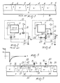
- Figure 1 illustrates the cross section of a semiconductor wafer in which a circuit for driving inductive loads, with P-type substrate, is provided.
- 1 indicates the P-type substrate
- 2-5 indicate different epitaxial wells of N ⁇ -type conductivity, mutually separated and isolated by means of the P-type isolation regions 6.
- the P substrate is clamped to the earth and forms with the epitaxial wells P-N junctions 2-5 which must be inversely biased to keep the various epitaxial wells isolated from one another.
- Said wells then accommodate the various layers and the various regions of semiconductor material with alternate conductivity type so as to obtain a complete driving integrated circuit, such as for example illustrated in figure 2 and generally indicated at 10.
- the driving integrated circuit 10 essentially comprises a stage 11 which can be configured differently, according to the required functions, to drive a power element 13 in turn intended to drive an external load.
- the integrated circuit 10 furthermore comprises a power supply, here represented by a voltage source 12, a terminal whereof (connected to a circuit pad 15, constituting the reference output of the circuit) represents the ground of the circuit, and the other terminal whereof is connected to the different components of the driving stage 11 to supply them.
- the power transistor 13 is connected with its collector to a supply voltage V cc and with its emitter to a contact pad 14 constituting the output terminal of the driving circuit.
- Said output terminal is connected to a terminal of the inductive load 16, the other terminal whereof is connected to the earth 17.
- the transistor 13 when the transistor 13 is controlled by the driving stage 11 so as to supply a positive current to the load 16, the latter remains at positive voltage, while when the transistor 13 is switched off, a negative overvoltage forms across the inductor 16, as illustrated in figure 3.
- one of the epitaxial wells constituting the device may reach a voltage which is lower than that of the substrate, which condition, as mentioned, is to be avoided.
- the invention teaches to bias the substrate at the output potential when the latter becomes negative, for example in the manner illustrated in figure 4.
- the driving integrated circuit 20 again comprises a driving stage 11, a power supply 12, a power transistor 13 as well as output 14 and reference 15 terminals for connection to two different terminals of the inductive load 16 referred to the earth 17.
- the substrate, indicated at 30, is not clamped to the ground and then to the external earth of the system, but three diodes 21, 22 and 23 are provided to electrically separate or connect the substrate from or to the output and from or to the earth of the system, according to the operating state.
- the circuit 20 has a first diode 21 connected with its anode to the substrate 30 and with its cathode to the output terminal 14, a second diode 22 connected with its anode to the substrate 30 and with its cathode to the reference terminal 15 and a third diode 23 connected with its anode to the internal ground 24 of the system and with its cathode to the reference terminal 15.
- the diode 21 is inversely biased, while the diodes 22 and 23 are forward biased. Therefore the current of the substrate flows through the diode 22 towards the earth. In this case (the drop on the diodes 22 and 23 being approximately equal) the potential of the ground 24 is equal to the potential of the substrate and all the epitaxial wells are mutually isolated.
- the power transistor is switched off and the output voltage becomes negative, the diode 21 is forward biased (thus connecting the substrate to the output terminal) while the diode 22 is inversely biased, separating the substrate from the earth 17. Then the substrate current flows through the diode 21, biasing the substrate 30 at a voltage equal to the (negative) output voltage minus the drop on the diode 21.
- FIG. 5 An embodiment of the circuit of figure 4 is illustrated in figure 5, showing the substrate 30 with P-type polarity and the different epitaxial wells 31-35 with N ⁇ -type conductivity mutually separated by the P-type isolation regions 36.
- the epitaxial wells 31 and 35 are provided for the accommodation of the different layers which form the components of the driving stage 11, while the epitaxial wells 32, 33 and 34 are intended for accommodating the diodes 21, 22 and 23.
- the epitaxial well 32 accommodates the P-type base region 37 (defining a circuit ground region) inside which the N+-type emitter region 38 is arranged, forming with the previous one the diode 23.
- the base region 37 is connected to the ground of the system, here indicated by the terminal 24, while the region 38 is electrically connected through line 42 to the reference terminal 15 of the circuit.
- the epitaxial well 33 forming with the substance 30 the diode 22, comprises in its interior the N+-type region 39 for connection to the output terminal 15 in turn connected to the external earth potential of the circuit.
- the epitaxial well 34 forming with the substrate 30 the diode 21, comprises in its interior the N+-type region 40 connected to the output terminal 14 at the voltage V out .
- the substrate has a lower potential than all the epitaxial wells referred to the ground 24, so that an effective separation and isolation thereof is achieved.
- the epitaxial well 34/substrate 30 junction is forward biased, linking the substrate 30 to said output voltage (apart from the drop on the diode 21 formed by said junction). Accordingly the current in the substrate can be reliably discharged through the output terminal, without affecting the other epitaxial wells of the driving stage.
- the invention fully achieves the intended aim and objects.
- a driving integrated circuit has been provided which operates reliably regardless of the output voltage of the circuit.
- the presented solution is simple, cheap, and producible by means of current methods, without requiring a substantial increase in the occupied area.
Landscapes
- Bipolar Integrated Circuits (AREA)
- Electronic Switches (AREA)
- Semiconductor Integrated Circuits (AREA)
Claims (5)
- Circuit intégré de pilotage de charges inductives comprenant au moins un substrat semiconducteur (30) de type de conductivité P et une pluralité de régions épitaxiales isolées (31-35) de type de conductivité N dans ce substrat ; ce circuit intégré ayant au moins une borne de sortie (14) réalisée au niveau de l'une des régions épitaxiales isolées (31-35) et connectée à une charge inductive (16) et une borne de référence (15) connectée à un potentiel de référence (17), cette borne de sortie (14) ayant un potentiel de sortie variable ; ce circuit intégré comprenant en outre un premier moyen de diode (21) ayant son anode connectée au substrat (30) et sa cathode connectée à la borne de sortie (14) et un deuxième moyen de diode (22) ayant son anode connectée au substrat (30) et sa cathode connectée à la borne de référence (15) pour connecter le substrat (30) à la borne de référence (15) quand le potentiel de sortie est supérieur au potentiel de référence et pour connecter le substrat (30) à la borne de sortie (14) quand le potentiel de sortie devient inférieur au potentiel de référence.
- Circuit intégré selon la revendication 1, caractérisé en ce qu'il comprend un troisième moyen de diode (23) interposé entre la borne de référence (15) et une région du circuit constituant une région de masse du circuit (37).
- Circuit intégré selon la revendication 2, caractérisé en ce que le troisième moyen de diode (23) a son anode connectée à la région de masse (37) et sa cathode connectée à la borne de référence (15).
- Circuit intégré selon une ou plusieurs des revendications précédentes, caractérisé en ce qu'il comprend une première région épitaxiale isolée (34) connectée à la borne de sortie (14), une deuxième région épitaxiale isolée (33) connectée à la borne de référence (15) et une troisième région épitaxiale isolée (32) contenant la région de masse (37).
- Circuit intégré selon la revendication 4, caractérisé en ce que la première région épitaxiale isolée (34) forme avec le substrat (30) le premier moyen de diode (21), en ce que la deuxième région épitaxiale isolée (33) forme avec le substrat (30) le deuxième moyen de diode (22) et en ce que la troisième région épitaxiale isolée (32) forme avec le substrat (30) le troisième moyen de diode (23).
Applications Claiming Priority (2)
| Application Number | Priority Date | Filing Date | Title |
|---|---|---|---|
| IT8719921A IT1215402B (it) | 1987-03-31 | 1987-03-31 | Circuito integrato di pilotaggio di carichi induttivi riferiti a terra. |
| IT1992187 | 1987-03-31 |
Publications (3)
| Publication Number | Publication Date |
|---|---|
| EP0284979A2 EP0284979A2 (fr) | 1988-10-05 |
| EP0284979A3 EP0284979A3 (en) | 1990-06-13 |
| EP0284979B1 true EP0284979B1 (fr) | 1993-06-23 |
Family
ID=11162350
Family Applications (1)
| Application Number | Title | Priority Date | Filing Date |
|---|---|---|---|
| EP88104635A Expired - Lifetime EP0284979B1 (fr) | 1987-03-31 | 1988-03-23 | Circuit intégré pour commander des charges inductives |
Country Status (5)
| Country | Link |
|---|---|
| US (1) | US4905067A (fr) |
| EP (1) | EP0284979B1 (fr) |
| JP (1) | JP2614076B2 (fr) |
| DE (1) | DE3881928T2 (fr) |
| IT (1) | IT1215402B (fr) |
Families Citing this family (14)
| Publication number | Priority date | Publication date | Assignee | Title |
|---|---|---|---|---|
| US4998160A (en) * | 1989-01-23 | 1991-03-05 | Motorola, Inc. | Substrate power supply contact for power integrated circuits |
| ATE171565T1 (de) * | 1992-06-30 | 1998-10-15 | St Microelectronics Srl | Struktur zur vermeidung des durchschaltens einer parasitären diode, die sich in einer epitaktischen wanne von integrierten schaltungen befindet |
| DE4333359C2 (de) * | 1993-06-26 | 2002-08-14 | Bosch Gmbh Robert | Monolithisch integrierte Leistungsendstufe |
| DE4411869C2 (de) * | 1994-04-06 | 1997-05-15 | Siemens Ag | Schaltungsanordnung mit einer integrierten Treiberschaltungsanordnung |
| DE19518524C2 (de) * | 1995-05-19 | 1997-03-20 | Siemens Ag | Schaltungsanordnung zur Verringerung einer Minoritätsträgerinjektion in ein Substrat |
| JP3513610B2 (ja) * | 1996-04-19 | 2004-03-31 | 株式会社ルネサステクノロジ | 半導体装置 |
| JP3513609B2 (ja) * | 1996-04-19 | 2004-03-31 | 株式会社ルネサステクノロジ | 半導体装置 |
| JP4128700B2 (ja) * | 1999-09-08 | 2008-07-30 | ローム株式会社 | 誘導性負荷駆動回路 |
| US6346461B1 (en) * | 2000-05-15 | 2002-02-12 | The Regents Of The University Of California | Electroless epitaxial etching for semiconductor applications |
| US6917095B1 (en) | 2000-05-30 | 2005-07-12 | Altera Corporation | Integrated radio frequency circuits |
| WO2005031958A1 (fr) * | 2003-09-30 | 2005-04-07 | Koninklijke Philips Electronics, N.V. | Circuits integres d'interface pour transistors de puissance a effet de champ a module regulateur de tension integre |
| KR101418396B1 (ko) * | 2007-11-19 | 2014-07-10 | 페어차일드코리아반도체 주식회사 | 전력 반도체 소자 |
| US9893724B2 (en) * | 2015-07-31 | 2018-02-13 | Texas Instruments Incorporated | Isolated output switching circuit |
| KR101841127B1 (ko) * | 2017-08-10 | 2018-03-22 | 주식회사 애크멕스 | 반도체 스위치의 구동 장치 |
Family Cites Families (5)
| Publication number | Priority date | Publication date | Assignee | Title |
|---|---|---|---|---|
| BE754677A (fr) * | 1969-08-11 | 1971-01-18 | Rca Corp | Circuits integres fonctionnant sur courant |
| FR2217810A1 (fr) * | 1973-02-15 | 1974-09-06 | Motorola Inc | |
| US3940785A (en) * | 1974-05-06 | 1976-02-24 | Sprague Electric Company | Semiconductor I.C. with protection against reversed power supply |
| DE3507181A1 (de) * | 1985-03-01 | 1986-09-04 | IC - Haus GmbH, 6501 Bodenheim | Schaltungsanordnung zur vermeidung parasitaerer substrat-effekte in integrierten schaltkreisen |
| FR2613131B1 (fr) * | 1987-03-27 | 1989-07-28 | Thomson Csf | Circuit integre protege contre des surtensions |
-
1987
- 1987-03-31 IT IT8719921A patent/IT1215402B/it active
-
1988
- 1988-03-23 DE DE88104635T patent/DE3881928T2/de not_active Expired - Fee Related
- 1988-03-23 EP EP88104635A patent/EP0284979B1/fr not_active Expired - Lifetime
- 1988-03-25 US US07/173,213 patent/US4905067A/en not_active Expired - Lifetime
- 1988-03-29 JP JP63077936A patent/JP2614076B2/ja not_active Expired - Fee Related
Also Published As
| Publication number | Publication date |
|---|---|
| IT8719921A0 (it) | 1987-03-31 |
| JPS63265460A (ja) | 1988-11-01 |
| EP0284979A2 (fr) | 1988-10-05 |
| EP0284979A3 (en) | 1990-06-13 |
| DE3881928T2 (de) | 1993-10-07 |
| IT1215402B (it) | 1990-02-08 |
| JP2614076B2 (ja) | 1997-05-28 |
| DE3881928D1 (de) | 1993-07-29 |
| US4905067A (en) | 1990-02-27 |
Similar Documents
| Publication | Publication Date | Title |
|---|---|---|
| EP0505191B1 (fr) | Dispositif à semiconducteur avec une région n à basse concentration pour améliorer les propriétés dV/dt | |
| US4794441A (en) | Semiconductor switch circuit | |
| US5469103A (en) | Diode circuit for high speed switching transistor | |
| US4905067A (en) | Integrated circuit for driving inductive loads | |
| KR20010015835A (ko) | 반도체 장치 | |
| US6878996B2 (en) | MOS power transistor | |
| US20130300487A1 (en) | Semiconductor switch | |
| US6218709B1 (en) | Semiconductor device and semiconductor circuit using the same | |
| US6248616B1 (en) | Method for suppressing parasitic effects in a junction-isolation integrated circuit | |
| EP0449093B1 (fr) | Dispositif de circuit pour prévenir les phénomènes de verrouillage dans des transistors PNP verticaux à collecteurs isolés | |
| JP2001507524A (ja) | ハーフブリッジ回路を具える半導体デバイス | |
| US4520277A (en) | High gain thyristor switching circuit | |
| EP0375037B1 (fr) | Protection de circuit intégré de puissance contre les surtensions de charge | |
| US5357157A (en) | Power MOSFET circuit including short circuiting means for detecting the potential of the source terminal | |
| EP0045310B1 (fr) | Circuit de commande utilisant un transistor de rabattement pour des commutateurs a semi-conducteurs de haute tension | |
| EP0624906B1 (fr) | Structure de circuit intégré pour la protection de dispositifs de puissance contre des surtensions | |
| US5300805A (en) | Epitaxial tub bias structure for integrated circuits | |
| US5045909A (en) | Power switching semiconductor device | |
| JPH08195490A (ja) | 誘導性負荷に電源供給、再循環および減磁を行なうための半導体素子 | |
| US5751052A (en) | Inductive driver circuit and method therefor | |
| KR102789733B1 (ko) | 전력 반도체 소자 | |
| US6369640B1 (en) | Zero crossing control structure for a bidirectional switch with a stable threshold | |
| EP0630051B1 (fr) | Structure intégrée d'un transistor bipolaire ou commutation ayant un temps d'emmagasinage contrÔlé | |
| EP0607474B1 (fr) | Circuit intégré semi-conducteur avec une couche pour l'isolation d'éléments dans un substrat | |
| US20020109151A1 (en) | Integrated device in emitter-switching configuration and related manufacturing process |
Legal Events
| Date | Code | Title | Description |
|---|---|---|---|
| PUAI | Public reference made under article 153(3) epc to a published international application that has entered the european phase |
Free format text: ORIGINAL CODE: 0009012 |
|
| AK | Designated contracting states |
Kind code of ref document: A2 Designated state(s): DE FR GB NL SE |
|
| PUAL | Search report despatched |
Free format text: ORIGINAL CODE: 0009013 |
|
| AK | Designated contracting states |
Kind code of ref document: A3 Designated state(s): DE FR GB NL SE |
|
| 17P | Request for examination filed |
Effective date: 19900620 |
|
| 17Q | First examination report despatched |
Effective date: 19920204 |
|
| RAP1 | Party data changed (applicant data changed or rights of an application transferred) |
Owner name: SGS-THOMSON MICROELECTRONICS S.R.L. |
|
| GRAA | (expected) grant |
Free format text: ORIGINAL CODE: 0009210 |
|
| AK | Designated contracting states |
Kind code of ref document: B1 Designated state(s): DE FR GB NL SE |
|
| REF | Corresponds to: |
Ref document number: 3881928 Country of ref document: DE Date of ref document: 19930729 |
|
| ET | Fr: translation filed | ||
| PLBE | No opposition filed within time limit |
Free format text: ORIGINAL CODE: 0009261 |
|
| STAA | Information on the status of an ep patent application or granted ep patent |
Free format text: STATUS: NO OPPOSITION FILED WITHIN TIME LIMIT |
|
| 26N | No opposition filed | ||
| EAL | Se: european patent in force in sweden |
Ref document number: 88104635.3 |
|
| REG | Reference to a national code |
Ref country code: FR Ref legal event code: D6 |
|
| REG | Reference to a national code |
Ref country code: GB Ref legal event code: IF02 |
|
| PGFP | Annual fee paid to national office [announced via postgrant information from national office to epo] |
Ref country code: SE Payment date: 20020306 Year of fee payment: 15 |
|
| PGFP | Annual fee paid to national office [announced via postgrant information from national office to epo] |
Ref country code: FR Payment date: 20020312 Year of fee payment: 15 |
|
| PGFP | Annual fee paid to national office [announced via postgrant information from national office to epo] |
Ref country code: GB Payment date: 20020327 Year of fee payment: 15 |
|
| PGFP | Annual fee paid to national office [announced via postgrant information from national office to epo] |
Ref country code: NL Payment date: 20020328 Year of fee payment: 15 |
|
| PGFP | Annual fee paid to national office [announced via postgrant information from national office to epo] |
Ref country code: DE Payment date: 20020404 Year of fee payment: 15 |
|
| PG25 | Lapsed in a contracting state [announced via postgrant information from national office to epo] |
Ref country code: GB Free format text: LAPSE BECAUSE OF NON-PAYMENT OF DUE FEES Effective date: 20030323 |
|
| PG25 | Lapsed in a contracting state [announced via postgrant information from national office to epo] |
Ref country code: SE Free format text: LAPSE BECAUSE OF NON-PAYMENT OF DUE FEES Effective date: 20030324 |
|
| PG25 | Lapsed in a contracting state [announced via postgrant information from national office to epo] |
Ref country code: NL Free format text: LAPSE BECAUSE OF NON-PAYMENT OF DUE FEES Effective date: 20031001 Ref country code: DE Free format text: LAPSE BECAUSE OF NON-PAYMENT OF DUE FEES Effective date: 20031001 |
|
| EUG | Se: european patent has lapsed | ||
| GBPC | Gb: european patent ceased through non-payment of renewal fee |
Effective date: 20030323 |
|
| PG25 | Lapsed in a contracting state [announced via postgrant information from national office to epo] |
Ref country code: FR Free format text: LAPSE BECAUSE OF NON-PAYMENT OF DUE FEES Effective date: 20031127 |
|
| NLV4 | Nl: lapsed or anulled due to non-payment of the annual fee |
Effective date: 20031001 |
|
| REG | Reference to a national code |
Ref country code: FR Ref legal event code: ST |