EP0285264A2 - Méthode de placement de blocs sur un support - Google Patents
Méthode de placement de blocs sur un support Download PDFInfo
- Publication number
- EP0285264A2 EP0285264A2 EP88301830A EP88301830A EP0285264A2 EP 0285264 A2 EP0285264 A2 EP 0285264A2 EP 88301830 A EP88301830 A EP 88301830A EP 88301830 A EP88301830 A EP 88301830A EP 0285264 A2 EP0285264 A2 EP 0285264A2
- Authority
- EP
- European Patent Office
- Prior art keywords
- block
- blocks
- positions
- placement
- geometrical
- Prior art date
- Legal status (The legal status is an assumption and is not a legal conclusion. Google has not performed a legal analysis and makes no representation as to the accuracy of the status listed.)
- Withdrawn
Links
Images



Classifications
-
- G—PHYSICS
- G06—COMPUTING OR CALCULATING; COUNTING
- G06F—ELECTRIC DIGITAL DATA PROCESSING
- G06F30/00—Computer-aided design [CAD]
- G06F30/30—Circuit design
- G06F30/39—Circuit design at the physical level
- G06F30/392—Floor-planning or layout, e.g. partitioning or placement
Definitions
- This invention relates to a method of placing blocks on a carrier, and in particular to testing a possible interchange of two blocks in order to determine whether the placement can be improved.
- CAD computer-aides design
- Data defining various attributes of the blocks, including the shape and size of each block, the locations of terminals of the block, and the connections that are required among the terminals of the blocks, is specified to a CAD system.
- Implementation is concerned with using the CAD system to bring the product of the system design stage to practical application.
- a placement phase takes place.
- data base files are created in which locations of the blocks on the integrated circuit die are defined such that there are no overlaps of blocks and economical use is made of the die area. Open spaces between blocks are reserved for channels to accommodate wiring connections among the terminals.
- a global routing phase takes place.
- the connections among the terminals are assigned to specific channels and the data base files are updated with data reflecting these channel assignments. The precise route that a connection takes through a channel is thereafter defined in a detail routing phase, and the data base files are updated accordingly.
- the data base files of the CAD system contain information defining the positions of the blocks on the die, the positions of the terminals of the blocks, and the paths followed by the connections among the blocks. These data base files are used when making the masks that are used in fabrication of the integrated circuit.
- the CAD system In order to maintain the volume of data to be stored and processed within manageable limits, the CAD system requires that all features that are defined in a plane parallel to the surface of the die be oriented along one of two orthogonal directions, normally referred to the horizontal or X direction and the vertical or Y direction.
- the success with which a CAD system may be used to aid in fabrication of an integrated circuit depends at a first level on being able to complete the design and this in turn depends upon the CAD system's being able to route all the connections that are defined in the system design stage within the channels that are defined in the placement phase.
- the success depends on minimizing the total length of wire necessary to complete the connections. Minimization of wire length is desirable in the case of an integrated circuit employing standard cells, because this implies that the size of the die is minimized, and is desirable in the case of an integrated circuit employing gate arrays because it implies that more space is available on the die for providing connections. Therefore, it is desirable to test the placement of the blocks on the die to determine whether it can be modified in a manner such that the total wire length is reduced. Accordingly, the placement phase is typically performed in two parts, namely constructive initial placement and iterative improvement placement.
- Constructive initial placement begins with all or some of the blocks unplaced and determines an initial or trial location for each block on the carrier.
- a placement slot is associated with each block. Each slot is defined with respect to both its position on the carrier and its size.
- a pair of blocks are interchanged between their respective placement slots, and a determination is made as to whether the new placement is better than the previous placement, i.e. results in a reduction in total wire length. If the new placement is not better than the previous placement, it is rejected and the blocks are returned to the slots that they occupied before the interchange. If, on the other hand, the new placement is better than the previous placement, the new placement is adopted and becomes the previous placement for the next interchange.
- placement slots for receiving blocks limits the interchanges that are considered to those which avoid overlap of blocks and other problems.
- a known scoring metric is the net half-perimeter metric.
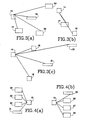
- terminals 2, 4, 6, 8 and 10 which are connected by a net, are illustrated.
- the net half-perimeter, or NHP, for a given net is defined as the sum of the horizontal and vertical extents of the bounding rectangle 12 of that net.
- the term “NHP” is used hereafter by itself to designate the net half-perimeter for a single net in a particular placement
- the term “block NHP” is used to designate the sum of the NHPs for all nets with terminals on a particular block in a particular placement
- the term “placement NHP” is used to designate the sum of all the NHPs for all the nets in a particular placement. Assuming that at least one net has terminals on more than one block, the placement NHP is not equal to the sum of the block NHPs.
- an initial placement of blocks on a carrier is tested in order to determine whether the placement can be improved by interchanging a first block and a second block by first selecting a terminal of the first block and identifying blocks that are con nected to that terminal of the first block.
- a measure of the half-perimeter of a rectangle bounding the positions on the carrier of the first block and the blocks identified as being connected to the first block is computed, and a measure of the half-perimeter of a second rectangle bounding the positions on the carrier of the second block and the blocks identified as being connected to the first block is computed.
- the half-perimeter of the second rectangle is substracted from the half-perimeter of the first rectangle to yield a difference value.
- steps are carried out for all other terminals of the first block and for the second block.
- the sum of the difference values for the first block is added to the sum of the difference values for the second block to yield a test score. If the test score is negative, the placement is modified by interchanging the first block and the second block.
- FIG. 2 illustrates several blocks 14 . . . 28 disposed on a carrier 29.
- the blocks might be standard integrated circuit cells and the carrier might be an integrated circuit die.
- Each block is shown as having one or more terminals 30 whereby the block is connected to one or more other blocks, and in a practical application of the invention, each block would have many more than three terminals.
- Lines 32 represent the connections that are required between the terminals of the block 14 and terminals of the other blocks, and lines 34 represent the connections that are required between the terminals of the block 15 and terminals of the other blocks.
- the blocks 14 and 15 are the same size and it is desired to determine whether interchanging these blocks will reduce the total wire length required to connect the blocks 14 . . . 28.
- connection might be required between two terminals of the same block, but this possibility is not illustrated in FIG. 2 because the wire length required to complete such a connection is not changed when the block is interchanged with another block.
- the possibility of a net having more than one terminal on a given block is ignored, because the resulting connection is simply a connection between two terminals on the same block.
- Data representing the nature of each block, the position of each block relative to the origin O of a rectangular Cartesian coordinate system (X, Y), the position of each terminal, and the connections between terminals is applied to a CAD system such as is shown in FIG. 8 by way of an input device 40 and is stored in a data base memory 44 of the CAD system.
- the NHP for a particular net is the sum of the vertical and horizontal extents of the smallest rectangle and has its sides parallel to the axes of the coordinate system (X, Y) and that contains all the terminals of the net.
- each terminal of a given block will be assumed to be at a common reference point of the block.
- the reference point is selected according to a rule which produces a unique result for the block, e.g. the center of the block. This is shown in FIG. 5 for the net illustrated in FIG. 3(c).
- the NHP for a given net will be assumed to be equal to the sum of the vertical and horizontal extents of the smallest rectangle that contains the reference points corresponding to all the terminals of the net.
- the NHP of a net including the block 14 is given by: where (X1, Y1) are the coordinates of the reference point of the block 14.
- the change in the NHP when the block 14 is moved to the position (X2, Y2) of the block 15 is:
- the quantity of interest is the change in the sum of the block NHPs for the blocks 14 and 15 when the two blocks are interchanged. This change, which is represented by DELNHP, can be computed by executing the following routine If the final value of DELNHP is less than zero, the interchange is accepted, otherwise it is rejected and the next interchange is evaluated.
- HZHALF, VTHALF, HZMID and VTMID can all be derived from the coordinates of two diagonally opposite corners of the new bounding rectangle. Therefore it is only necessary to store and update, for each net having a terminal on each block, the coordinates of two points in order to enable computation of the change in sum of the block NHPs when two blocks are interchanged.
- FIG. 7 A potential interchange between two blocks 51 and 52 is being evaluated.
- a first net indicated by solid connecting lines in FIG. 7(a) has terminals on the blocks 51 . . . 54, and is therefore a doubly-represented net.
- the bounding rectangle 57 for the first net, omitting the block 51 is illustrated in solid lines in FIG. 7(a) and the bounding rectangle 58 for the first net without the block 52 is illustrated in dot-dashed lines in FIG. 7(b).
- a second net indicated by dashed connecting lines in FIG. 7(a) has terminals on the blocks 51, 55 and 56 and the bounding rectangle 59 for the second net, again omitting the block 51, as illustrated in dashed lines. Since the blocks 51 and 52 are within the boundaries of the rectangles 59 and 58 respectively, the rectangles 59 and 58 are in fact the same size as the bounding rectangles for the entire second and first nets respectively. It will be assumed that no other nets are involved.
- the change in NHPs for the first and second nets when the block 51 is moved to the position of the block 52 is computed, and the change in NHP for the first net when the block 52 is moved to the position of the block 51 is computed.
- the block 51 is outside the rectangle 57, and therefore the NHP for the first net decreases when the block 51 is moved to the position of the block 52. Because the block 52 is within the boundary of the rectangle 58, there is no change in the NHP for the second net when the block 51 is moved to the position of the block 52. On the other hand, the NHP for the first net is not changed when the block 52 is moved to the position of the block 51.
- the interchange of the blocks 51 and 52 results in a decrease in the placement NHP. Then, the existence of the doubly-represented net is identified and the illusory improvement is computed by determining the decrease in placement NHP that is attributable to the apparent decrease in the NHP for the first net on moving the block 51 to the position of the block 52. If this is less than the total decrease in placement NHP, it implies that the interchange resulted in a decrease in placement NHP even taking account of the doubly-represented net.
- a program defining the method is stored in a program memory 46.
- a processor 42 operates under control of the program to execute the described method and update the data base files stored in the memory 44, and the updated data base files are made available by way of an output device 48.
- the method will be performed about three million times.
Landscapes
- Engineering & Computer Science (AREA)
- Computer Hardware Design (AREA)
- Physics & Mathematics (AREA)
- Theoretical Computer Science (AREA)
- Architecture (AREA)
- Evolutionary Computation (AREA)
- Geometry (AREA)
- General Engineering & Computer Science (AREA)
- General Physics & Mathematics (AREA)
- Design And Manufacture Of Integrated Circuits (AREA)
- Testing Or Measuring Of Semiconductors Or The Like (AREA)
- Semiconductor Integrated Circuits (AREA)
Applications Claiming Priority (2)
| Application Number | Priority Date | Filing Date | Title |
|---|---|---|---|
| US3329087A | 1987-04-02 | 1987-04-02 | |
| US33290 | 1987-04-02 |
Publications (2)
| Publication Number | Publication Date |
|---|---|
| EP0285264A2 true EP0285264A2 (fr) | 1988-10-05 |
| EP0285264A3 EP0285264A3 (fr) | 1989-03-15 |
Family
ID=21869571
Family Applications (1)
| Application Number | Title | Priority Date | Filing Date |
|---|---|---|---|
| EP88301830A Withdrawn EP0285264A3 (fr) | 1987-04-02 | 1988-03-02 | Méthode de placement de blocs sur un support |
Country Status (2)
| Country | Link |
|---|---|
| EP (1) | EP0285264A3 (fr) |
| JP (1) | JPS63262765A (fr) |
Family Cites Families (1)
| Publication number | Priority date | Publication date | Assignee | Title |
|---|---|---|---|---|
| JPS59154055A (ja) * | 1983-02-22 | 1984-09-03 | Hitachi Ltd | 論理回路基板上の素子配置方法 |
-
1988
- 1988-03-02 EP EP88301830A patent/EP0285264A3/fr not_active Withdrawn
- 1988-03-23 JP JP63069205A patent/JPS63262765A/ja active Pending
Also Published As
| Publication number | Publication date |
|---|---|
| JPS63262765A (ja) | 1988-10-31 |
| EP0285264A3 (fr) | 1989-03-15 |
Similar Documents
| Publication | Publication Date | Title |
|---|---|---|
| US5801959A (en) | Integrated circuit layout | |
| US5251147A (en) | Minimizing the interconnection cost of electronically linked objects | |
| US5930499A (en) | Method for mixed placement of structured and non-structured circuit elements | |
| US6026228A (en) | Integrated circuit design method, database apparatus for designing integrated circuit and integrated circuit design support apparatus | |
| US5790841A (en) | Method for placement of clock buffers in a clock distribution system | |
| US5187668A (en) | Placement optimization system aided by cad | |
| US5113352A (en) | Integrating the logical and physical design of electronically linked objects | |
| US5818729A (en) | Method and system for placing cells using quadratic placement and a spanning tree model | |
| EP0367154A2 (fr) | Optimalisation de l'organisation de plusieurs éléments discrets | |
| US6735742B2 (en) | Method for optimizing a cell layout using parameterizable cells and cell configuration data | |
| EP0350353B1 (fr) | Méthode de traitement de données de layout | |
| EP0612023A2 (fr) | Procédé d'acheminement pour schéma de réseau | |
| US6086625A (en) | Method and apparatus for designing a circuit by describing logic design information with a hardware description language | |
| GB1445914A (en) | Apparatus for producing graphical data descriptive of an integrated circuit design | |
| Seiler | A hardware assisted design rule check architecture | |
| US8006215B1 (en) | Circuit clustering during placement | |
| EP0285264A2 (fr) | Méthode de placement de blocs sur un support | |
| JPH09223744A (ja) | Vlsiチップへの回路の配置方法 | |
| US6243850B1 (en) | Allocation apparatus and method for determining cell allocation of semiconductor circuit | |
| US6408426B1 (en) | Method for determining locations of interconnect repeater farms during physical design of integrated circuits | |
| US6792583B1 (en) | Information processing apparatus, information processing system, and storage media | |
| EP0218420A2 (fr) | Système de positionnement de composants à optimalisation de contrainte | |
| JP3166847B2 (ja) | プリント基板設計における配線収容性評価プログラムを記録した記録媒体および装置 | |
| JP3095307B2 (ja) | 電気部品自動配置装置及び電気部品の自動配置方法 | |
| JPH05121546A (ja) | 半導体集積回路のレイアウト方法 |
Legal Events
| Date | Code | Title | Description |
|---|---|---|---|
| PUAI | Public reference made under article 153(3) epc to a published international application that has entered the european phase |
Free format text: ORIGINAL CODE: 0009012 |
|
| AK | Designated contracting states |
Kind code of ref document: A2 Designated state(s): DE FR GB |
|
| PUAL | Search report despatched |
Free format text: ORIGINAL CODE: 0009013 |
|
| AK | Designated contracting states |
Kind code of ref document: A3 Designated state(s): DE FR GB |
|
| STAA | Information on the status of an ep patent application or granted ep patent |
Free format text: STATUS: THE APPLICATION IS DEEMED TO BE WITHDRAWN |
|
| 18D | Application deemed to be withdrawn |
Effective date: 19890916 |