EP0285894A1 - Bildaufnahmegerät - Google Patents
Bildaufnahmegerät Download PDFInfo
- Publication number
- EP0285894A1 EP0285894A1 EP88104506A EP88104506A EP0285894A1 EP 0285894 A1 EP0285894 A1 EP 0285894A1 EP 88104506 A EP88104506 A EP 88104506A EP 88104506 A EP88104506 A EP 88104506A EP 0285894 A1 EP0285894 A1 EP 0285894A1
- Authority
- EP
- European Patent Office
- Prior art keywords
- pixels
- signals
- reading
- imaging apparatus
- read
- Prior art date
- Legal status (The legal status is an assumption and is not a legal conclusion. Google has not performed a legal analysis and makes no representation as to the accuracy of the status listed.)
- Granted
Links
Images



Classifications
-
- H—ELECTRICITY
- H04—ELECTRIC COMMUNICATION TECHNIQUE
- H04N—PICTORIAL COMMUNICATION, e.g. TELEVISION
- H04N25/00—Circuitry of solid-state image sensors [SSIS]; Control thereof
- H04N25/70—SSIS architectures; Circuits associated therewith
- H04N25/76—Addressed sensors, e.g. MOS or CMOS sensors
-
- H—ELECTRICITY
- H04—ELECTRIC COMMUNICATION TECHNIQUE
- H04N—PICTORIAL COMMUNICATION, e.g. TELEVISION
- H04N25/00—Circuitry of solid-state image sensors [SSIS]; Control thereof
- H04N25/40—Extracting pixel data from image sensors by controlling scanning circuits, e.g. by modifying the number of pixels sampled or to be sampled
- H04N25/44—Extracting pixel data from image sensors by controlling scanning circuits, e.g. by modifying the number of pixels sampled or to be sampled by partially reading an SSIS array
- H04N25/443—Extracting pixel data from image sensors by controlling scanning circuits, e.g. by modifying the number of pixels sampled or to be sampled by partially reading an SSIS array by reading pixels from selected two-dimensional [2D] regions of the array, e.g. for windowing or digital zooming
Definitions
- Fig. 1 is a schematic circuit diagram of an embodiment of the imaging apparatus in accordance with the present invention.
- the imaging apparatus has an imaging device having a multiplicity of photo-sensors 1 which are arranged in the form of a matrix constituted by m rows and n columns.
- the photo-sensor 1 may be of any type, such as destructive reading type, non-destructive reading type, MOS type, electrostatic induction type, base accumulation type, and so forth.
- the photo-sensors of each row are connected to a horizontal line HL.
- a plurality of rows of photo-sensors 1 are connected to corresponding horizontal lines HL, each of which is adapted to receive driving pulses ⁇ Rl and ⁇ R2 through transistors Q r1 and Q r2 respectively, whereby the lines of photo-sensors are driven independently for the purpose of reading of signals and resetting.
- the gates of the gate electrodes of the transistors Q r1 and Q r2 of each two adjacent horizontal lines are commonly connected and the common connections of these gate electrodes are connected to output terminals of a vertical scanning circuit 2 through transistors Q e and Q o which appear alternately for the successive horizontal lines HL.
- the vertical scanning circuit 2 starts the scanning operation in response to a start pulse ⁇ VS and successively outputs vertical scanning pulses in synchronization with the pulses ⁇ V1 and ⁇ V2.
- the columns of the photo-sensors 1 are connected to corresponding vertical lines VL, each of which is connected to temporary storage capacitors C1 and C2 through shifting transistors Q t1 and Q t2 .
- the capacitors C1 and C2 are connected to signal lines S1 and S2, through scanning transistors QS1 and QS2.
- the gate electrodes of the scanning transistors Q s1 and Q s2 of each pair are commonly connected and the common connections of the successive pairs of scanning transistors Q s1 and Q s2 receive scanning pulses from the horizontal scanning circuit 3. More specifically, the horizontal scanning circuit 3 starts the scanning operation in response to a start pulse ⁇ HS and outputs scanning pulses in synchronization with pulses ⁇ H1 and ⁇ H2.
- Each vertical line VL is grounded through a transistor Q vc which receives at its gate electrode a pulse ⁇ VC.
- the pulses ⁇ mentioned above are supplied from a driver 4 which is controlled by a control unit 5.
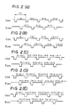
- the horizontal pixel lines covering the image portion 102 are scanned twice in a non-interlaced manner. More specifically, the scanning lines a , a+1 , a+2 , ...., b-1 , b are sequentially read from an odd-number field of the display, and the same lines a to b are read again for the even-number field of the display.
- a second type of operation illustrated in Fig. 2B, the reading is conducted by means of a photo-sensor which is capable of enabling a signal to be read in a non-destructive manner.
- the signal of the photo-sensor is not destroyed by the reading operation, and the pixel signals of each line are successively read twice.
- scanning lines are read as a , (a) , a+2 , (a+2) ,_... for the odd-number field of the display, where (a) , (a+2) , etc, each represents the second reading of the scanning line a , a+2 , etc.
- scanning lines are read as a+1 , (a+1) , a+3 , (a+3) ,...., as will be seen from Fig. 2B.
- Fig. 2E shows a fourth type of reading operation in which the double-line reading system is used with only one of each pair of scanning lines read in the non-destructive manner.
- the scanning lines are read as a ; a+1 ; ( a+1 ), a+2 ,... for the odd-number field, whereas, scanning lines are read as ( a+1 ), a+2 ; ( a+2 ), a+3 ;... for the even-number field.
- Fig. 3 is a schematic timing chart illustrating the operation of the vertical scanning circuit driven by the driver 4 in the zoom-out reading mode.
- the transistors Q t1 are turned off, while the transistors Q vc are turned on so as to ground the vertical lines VL. Then, the pulse ⁇ R1 is set high high so as to reset the photo-sensors of the scanning line a .
- the signals corresponding to the scanning line a stored in the capacitors C1 are scanned by the horizontal scanning circuit 3 and are sequentially shifted to the signal line S1 through the transistors Q s1 .
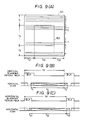
- the shifting of the signals is conducted in such a manner that, as explained before in connection with Fig. 9C, the signals from the unnecessary portions of the image are shifted at a high speed in the periods t21 and t23 within the horizontal blanking periods, whereas the signals corresponding to the image portion 102 to be zoomed out are shifted in the horizontal effective period t22.
- the pulses ⁇ V1 and ⁇ V2 are set low and high, respectively, so that the vertical scanning circuit 2 shifts the position of output of the scanning pulse to the next stage and outputs the scanning pulse for the next stage when the next pulse ⁇ V1 is set high.
- the scanning is executed in non-interlaced manner so that the signals from the scanning lines a , a+1 , a+2 ,... are sequentially read for the even number field, while the same lines a+1 , a+2 ,... are read once again for the even number field.
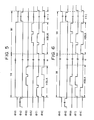
- Fig. 5 is a timing chart illustrating another practical example of the first type of operation explained before in connection with Fig. 2A.
- the field selection pulse ⁇ FE is maintained at high level so that only the transistors Q e are turned on, and the non-interlaced scanning is executed only by means of the pulses ⁇ R1 and ⁇ R2.
- the pulse ⁇ V1 is set high so that the transistors Q r1 and Q r2 corresponding to the scanning lines a and a+1 are turned on.
- Fig. 6 is a timing chart illustrating a practical example of the second type of operation explained before in connection with Fig. 2B.
- This operation relies upon non- destructive reading of signals from the photo-sensors.
- the pulses ⁇ FE and ⁇ FO are inverted for each field.
- the pulse ⁇ FE is set high so as to turn the transistors Q e on.
- the pulse ⁇ V1 is set high so that the transistor Q r1 corresponding to the scanning line a is turned on.
- the capacitors C1 are cleared and the signals on the photo-sensors of the scanning line a are read in a non-destructive manner and stored in the capacitors C1.
- the photo-sensors are not reset because the signals carried by these sensors are read again in the next horizontal scanning period.
- the horizontal scanning is conducted by the horizontal scanning circuit 3 in the same manner as in the reading operations described before.
- the capacitors C1 are cleared in the next horizontal blanking period and the signals are read again from the photo-sensors of the scanning line a in accordance with the pulse ⁇ R1.
- the thus read signals are stored in the capacitors C1 and then the photo-sensors are reset. In consequence, the signals ( a ) read from the same scanning line a are scanned.
- the output position of the vertical scanning circuit 2 is shifted by one stage, and the operation described hereinbefore is conducted for the scanning line a+2 , so that signals a+2 , ( a+2 ). This operation is repeated for other scanning lines to be included in the odd-number field.
- the same pixels can be scanned twice by virtue of the non-destructive reading function of the photo-sensors. Therefore, the reduction in the vertical resolution zooming out of the image can be compensated for without requiring any specific additional signal processing circuit, although a level correcting operation is needed. In consequence, the construction of the circuit, as well as the signal processing operation, can be remarkably simplified.
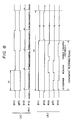
- Fig. 7 is a timing chart illustrating a practical example of the fourth type of operation described above. This operation is suitable for a color imaging apparatus which has a mosaic color filter provided on an imaging device having photo-sensors arranged in the manner shown in Fig. 1.
- pulses ⁇ V1 and ⁇ EF are set high, while the pulse ⁇ EO is set low, thereby turning on the transistors Q r1 and Q r2 corresponding to the scanning lines a and a+1 .
- the pulses ⁇ VC, ⁇ T1 and ⁇ T2 are set high, so as to turn on the transistors Q vc , Q t1 and Q t2 , thereby clearing the vertical lines VL, capacitors C1 and the capacitors C2.
- the transistors Q vc and Q t2 are turned off and the signals on the photo-sensors of the scanning line a are read in a non-destructive manner in accordance with the pulse ⁇ R1 and are stored in the capacitors C1.
- the pulses ⁇ FE and ⁇ FO are inverted so that the transistors Q o are turned on with the result that all the transistors Q r2 and Q r1 having gate electrodes connected to the transistors Q o are turned on, whereby the scanning lines a+1 and a+2 are selected.
- the capacitors C1 and C2 are cleared in this state and then the transistors Q t1 are turned on, so that the signals on the photo-sensors of the scanning line a+1 are read once again in accordance with the pulse ⁇ R1 and the thus read signals are stored in the capacitors C1.
- signals (a+1) and a+2 derived from the scanning lines a+1 and a+2 , stored in the capacitors C1 and C2, are scanned by the horizontal scanning circuit 3 and are sequentially output through the signal lines S1 and S2.
- FIGs. 8A and 8B are illustrations of vertical scanning and horizontal scanning of this mode of operation.
Landscapes
- Engineering & Computer Science (AREA)
- Multimedia (AREA)
- Signal Processing (AREA)
- Transforming Light Signals Into Electric Signals (AREA)
Applications Claiming Priority (2)
| Application Number | Priority Date | Filing Date | Title |
|---|---|---|---|
| JP77953/87 | 1987-03-31 | ||
| JP62077953A JPS63245073A (ja) | 1987-03-31 | 1987-03-31 | 撮像装置 |
Publications (2)
| Publication Number | Publication Date |
|---|---|
| EP0285894A1 true EP0285894A1 (de) | 1988-10-12 |
| EP0285894B1 EP0285894B1 (de) | 1993-09-01 |
Family
ID=13648373
Family Applications (1)
| Application Number | Title | Priority Date | Filing Date |
|---|---|---|---|
| EP88104506A Expired - Lifetime EP0285894B1 (de) | 1987-03-31 | 1988-03-21 | Bildaufnahmegerät |
Country Status (4)
| Country | Link |
|---|---|
| US (1) | US4876601A (de) |
| EP (1) | EP0285894B1 (de) |
| JP (1) | JPS63245073A (de) |
| DE (1) | DE3883577T2 (de) |
Cited By (1)
| Publication number | Priority date | Publication date | Assignee | Title |
|---|---|---|---|---|
| EP0391690A1 (de) * | 1989-04-04 | 1990-10-10 | SHARP Corporation | Bildaufnahmeeinrichtung mit elektronischer Bildvergrösserung |
Families Citing this family (15)
| Publication number | Priority date | Publication date | Assignee | Title |
|---|---|---|---|---|
| KR920003656B1 (ko) * | 1988-04-01 | 1992-05-06 | 샤프 가부시끼 가이샤 | 전자적으로 화상을 확대하여 촬영이 가능한 촬상 장치 |
| DE69033613T2 (de) * | 1989-05-31 | 2001-05-03 | Canon K.K., Tokio/Tokyo | Fotoelektrischer Umwandler |
| JPH03117275A (ja) * | 1989-09-29 | 1991-05-20 | Sanyo Electric Co Ltd | オートフォーカスカメラ |
| US5146339A (en) * | 1989-11-21 | 1992-09-08 | Canon Kabushiki Kaisha | Photoelectric converting apparatus employing Darlington transistor readout |
| JP2991354B2 (ja) * | 1990-11-07 | 1999-12-20 | キヤノン株式会社 | 画像読取装置およびそれを備えた画像情報処理装置 |
| KR930012203B1 (ko) * | 1991-01-09 | 1993-12-24 | 삼성전자 주식회사 | 특정부위 확대 녹화방법 및 장치 |
| JP3216907B2 (ja) * | 1992-05-18 | 2001-10-09 | 株式会社日立製作所 | 電子ズーム装置及び撮像装置 |
| DE69628187D1 (de) * | 1995-11-07 | 2003-06-18 | California Inst Of Techn | Bildsensor mit linearem ausgang mit grossem dynamikbereich |
| US6977684B1 (en) | 1998-04-30 | 2005-12-20 | Canon Kabushiki Kaisha | Arrangement of circuits in pixels, each circuit shared by a plurality of pixels, in image sensing apparatus |
| US6956605B1 (en) | 1998-08-05 | 2005-10-18 | Canon Kabushiki Kaisha | Image pickup apparatus |
| US6734906B1 (en) | 1998-09-02 | 2004-05-11 | Canon Kabushiki Kaisha | Image pickup apparatus with photoelectric conversion portions arranged two dimensionally |
| JP2001024949A (ja) | 1999-07-08 | 2001-01-26 | Canon Inc | 固体撮像装置及びそれを用いた撮像システム |
| JP3548465B2 (ja) | 1999-09-08 | 2004-07-28 | キヤノン株式会社 | 撮像装置及び撮像方法 |
| JP3937716B2 (ja) | 2000-10-24 | 2007-06-27 | キヤノン株式会社 | 固体撮像装置及び撮像システム |
| JP2006311051A (ja) * | 2005-04-27 | 2006-11-09 | Matsushita Electric Ind Co Ltd | 固体撮像素子用の信号処理回路および固体撮像装置 |
Citations (5)
| Publication number | Priority date | Publication date | Assignee | Title |
|---|---|---|---|---|
| US4002824A (en) * | 1976-01-28 | 1977-01-11 | The United States Of America As Represented By The Secretary Of The Navy | Selective zoom camera and display |
| DE2913116A1 (de) * | 1979-04-02 | 1980-10-23 | Bosch Gmbh Robert | Verfahren zum auslesen von festkoerper- bildsensoren und schaltungsanordnung zur durchfuehrung des verfahrens |
| US4527200A (en) * | 1982-02-10 | 1985-07-02 | Hitachi, Ltd. | Solid state imaging device |
| US4658287A (en) * | 1984-02-29 | 1987-04-14 | Fairchild Camera And Instrument Corp. | MOS imaging device with monochrome-color compatibility and signal readout versatility |
| FR2588709A1 (fr) * | 1985-10-16 | 1987-04-17 | Thomson Csf | Systeme de grossissement d'une partie d'une image dans les dispositifs de prise de vues video notamment a senseur a transfert de charges |
Family Cites Families (11)
| Publication number | Priority date | Publication date | Assignee | Title |
|---|---|---|---|---|
| US3935381A (en) * | 1974-06-24 | 1976-01-27 | The United States Of America As Represented By The Secretary Of The Navy | Electronic solid state sensor image size control |
| DE2725362C3 (de) * | 1977-06-04 | 1980-08-28 | Robert Bosch Gmbh, 7000 Stuttgart | Verfahren zum Verarbeiten von Farbfernsehsignalen |
| JPS57178479A (en) * | 1981-04-27 | 1982-11-02 | Sony Corp | Solid image pickup element |
| US4546349A (en) * | 1981-09-29 | 1985-10-08 | Sperry Corporation | Local zoom for raster scan displays |
| EP0119742B2 (de) * | 1983-02-15 | 1992-12-16 | Sharp Kabushiki Kaisha | Zweidimensionale Bildlesevorrichtung |
| JPS6032488A (ja) * | 1983-08-02 | 1985-02-19 | Canon Inc | 撮像装置 |
| JPS60160780A (ja) * | 1984-01-31 | 1985-08-22 | Nec Corp | 特殊効果用画像記憶装置 |
| FR2566219B1 (fr) * | 1984-06-15 | 1989-04-28 | Sfim | Procede et dispositif pour l'exploration d'une fenetre de la zone image d'un dispositif a transfert de charges du type a transfert de trames |
| US4706122A (en) * | 1984-08-30 | 1987-11-10 | Nec Corporation | Solid-state imaging device compatible with different television systems |
| GB2170974B (en) * | 1985-02-07 | 1988-01-06 | Rank Cintel Ltd | Telecine projector line array sensor |
| JPH0642726B2 (ja) * | 1985-10-18 | 1994-06-01 | キヤノン株式会社 | 固体撮像装置 |
-
1987
- 1987-03-31 JP JP62077953A patent/JPS63245073A/ja active Pending
-
1988
- 1988-03-15 US US07/168,176 patent/US4876601A/en not_active Expired - Lifetime
- 1988-03-21 DE DE88104506T patent/DE3883577T2/de not_active Expired - Fee Related
- 1988-03-21 EP EP88104506A patent/EP0285894B1/de not_active Expired - Lifetime
Patent Citations (5)
| Publication number | Priority date | Publication date | Assignee | Title |
|---|---|---|---|---|
| US4002824A (en) * | 1976-01-28 | 1977-01-11 | The United States Of America As Represented By The Secretary Of The Navy | Selective zoom camera and display |
| DE2913116A1 (de) * | 1979-04-02 | 1980-10-23 | Bosch Gmbh Robert | Verfahren zum auslesen von festkoerper- bildsensoren und schaltungsanordnung zur durchfuehrung des verfahrens |
| US4527200A (en) * | 1982-02-10 | 1985-07-02 | Hitachi, Ltd. | Solid state imaging device |
| US4658287A (en) * | 1984-02-29 | 1987-04-14 | Fairchild Camera And Instrument Corp. | MOS imaging device with monochrome-color compatibility and signal readout versatility |
| FR2588709A1 (fr) * | 1985-10-16 | 1987-04-17 | Thomson Csf | Systeme de grossissement d'une partie d'une image dans les dispositifs de prise de vues video notamment a senseur a transfert de charges |
Cited By (1)
| Publication number | Priority date | Publication date | Assignee | Title |
|---|---|---|---|---|
| EP0391690A1 (de) * | 1989-04-04 | 1990-10-10 | SHARP Corporation | Bildaufnahmeeinrichtung mit elektronischer Bildvergrösserung |
Also Published As
| Publication number | Publication date |
|---|---|
| EP0285894B1 (de) | 1993-09-01 |
| DE3883577D1 (de) | 1993-10-07 |
| US4876601A (en) | 1989-10-24 |
| JPS63245073A (ja) | 1988-10-12 |
| DE3883577T2 (de) | 1994-02-17 |
Similar Documents
| Publication | Publication Date | Title |
|---|---|---|
| US4876601A (en) | Imaging apparatus having zoom capability via readout variation | |
| JP3551571B2 (ja) | カラーccd固体撮像素子 | |
| US6496224B2 (en) | Imaging device including thinned read out mode and all pixel read out mode | |
| JPH0529192B2 (de) | ||
| US5420631A (en) | Solid state image pickup device and method | |
| JPH0522668A (ja) | 固体撮像装置 | |
| JP3920085B2 (ja) | 固体撮像装置とそのスミア補正方法並びにデジタルスチルカメラ | |
| JP3353921B2 (ja) | 固体撮像装置 | |
| EP0449210B1 (de) | Elektronische Zoomeinrichtung | |
| US4298891A (en) | Television receiver | |
| US6356305B1 (en) | Image-pickup apparatus and method for reading accumulated signal changes through transfer lines | |
| US6760069B2 (en) | Method and apparatus for processing image signals | |
| US5434437A (en) | Solid state image sensor and its driving method | |
| KR100242781B1 (ko) | 촬상 장치 | |
| JPH0695735B2 (ja) | 固体撮像装置 | |
| US7535505B2 (en) | Imaging device and a digital camera having same in which pixel signals read from the pixel block are horizontally transferred in a collective fashion | |
| JPS6043704B2 (ja) | 固体撮像装置 | |
| US5998778A (en) | Focal plane array and driving method therefor | |
| JPS62291269A (ja) | 固体カラ−撮像装置 | |
| JPH09233394A (ja) | 撮像装置 | |
| US6355949B1 (en) | Solid state imaging apparatus with horizontal charge transfer register which can transfer signal charge faster | |
| JPH10285467A (ja) | 撮像装置 | |
| JP2000308075A (ja) | 撮像素子および撮像素子の駆動方法 | |
| JP2897665B2 (ja) | 固体撮像素子の駆動方法 | |
| JP3558505B2 (ja) | 固体撮像素子の駆動方法 |
Legal Events
| Date | Code | Title | Description |
|---|---|---|---|
| PUAI | Public reference made under article 153(3) epc to a published international application that has entered the european phase |
Free format text: ORIGINAL CODE: 0009012 |
|
| AK | Designated contracting states |
Kind code of ref document: A1 Designated state(s): DE FR GB IT NL |
|
| 17P | Request for examination filed |
Effective date: 19890222 |
|
| 17Q | First examination report despatched |
Effective date: 19910902 |
|
| GRAA | (expected) grant |
Free format text: ORIGINAL CODE: 0009210 |
|
| AK | Designated contracting states |
Kind code of ref document: B1 Designated state(s): DE FR GB IT NL |
|
| PG25 | Lapsed in a contracting state [announced via postgrant information from national office to epo] |
Ref country code: IT Free format text: LAPSE BECAUSE OF FAILURE TO SUBMIT A TRANSLATION OF THE DESCRIPTION OR TO PAY THE FEE WITHIN THE PRE;WARNING: LAPSES OF ITALIAN PATENTS WITH EFFECTIVE DATE BEFORE 2007 MAY HAVE OCCURRED AT ANY TIME BEFORE 2007. THE CORRECT EFFECTIVE DATE MAY BE DIFFERENT FROM THE ONE RECORDED.SCRIBED TIME-LIMIT Effective date: 19930901 Ref country code: NL Effective date: 19930901 |
|
| REF | Corresponds to: |
Ref document number: 3883577 Country of ref document: DE Date of ref document: 19931007 |
|
| ET | Fr: translation filed | ||
| NLV1 | Nl: lapsed or annulled due to failure to fulfill the requirements of art. 29p and 29m of the patents act | ||
| PG25 | Lapsed in a contracting state [announced via postgrant information from national office to epo] |
Ref country code: GB Effective date: 19940321 |
|
| PLBE | No opposition filed within time limit |
Free format text: ORIGINAL CODE: 0009261 |
|
| STAA | Information on the status of an ep patent application or granted ep patent |
Free format text: STATUS: NO OPPOSITION FILED WITHIN TIME LIMIT |
|
| 26N | No opposition filed | ||
| GBPC | Gb: european patent ceased through non-payment of renewal fee |
Effective date: 19940321 |
|
| PGFP | Annual fee paid to national office [announced via postgrant information from national office to epo] |
Ref country code: FR Payment date: 20060308 Year of fee payment: 19 |
|
| PGFP | Annual fee paid to national office [announced via postgrant information from national office to epo] |
Ref country code: DE Payment date: 20060316 Year of fee payment: 19 |
|
| REG | Reference to a national code |
Ref country code: FR Ref legal event code: ST Effective date: 20071130 |
|
| PG25 | Lapsed in a contracting state [announced via postgrant information from national office to epo] |
Ref country code: DE Free format text: LAPSE BECAUSE OF NON-PAYMENT OF DUE FEES Effective date: 20071002 |
|
| PG25 | Lapsed in a contracting state [announced via postgrant information from national office to epo] |
Ref country code: FR Free format text: LAPSE BECAUSE OF NON-PAYMENT OF DUE FEES Effective date: 20070402 |