EP0286528A1 - Optisch integrierter Verschiebungssensor - Google Patents
Optisch integrierter Verschiebungssensor Download PDFInfo
- Publication number
- EP0286528A1 EP0286528A1 EP88400814A EP88400814A EP0286528A1 EP 0286528 A1 EP0286528 A1 EP 0286528A1 EP 88400814 A EP88400814 A EP 88400814A EP 88400814 A EP88400814 A EP 88400814A EP 0286528 A1 EP0286528 A1 EP 0286528A1
- Authority
- EP
- European Patent Office
- Prior art keywords
- mirror
- separating
- sensor according
- mobile
- layer
- Prior art date
- Legal status (The legal status is an assumption and is not a legal conclusion. Google has not performed a legal analysis and makes no representation as to the accuracy of the status listed.)
- Granted
Links
- 238000006073 displacement reaction Methods 0.000 title description 21
- 230000003287 optical effect Effects 0.000 claims abstract description 33
- 238000005259 measurement Methods 0.000 claims abstract description 19
- 235000012239 silicon dioxide Nutrition 0.000 claims abstract description 17
- 229910052581 Si3N4 Inorganic materials 0.000 claims abstract description 14
- 230000010363 phase shift Effects 0.000 claims abstract description 11
- 239000000463 material Substances 0.000 claims description 28
- 239000000758 substrate Substances 0.000 claims description 25
- HQVNEWCFYHHQES-UHFFFAOYSA-N silicon nitride Chemical compound N12[Si]34N5[Si]62N3[Si]51N64 HQVNEWCFYHHQES-UHFFFAOYSA-N 0.000 claims description 9
- 238000001020 plasma etching Methods 0.000 claims description 8
- 230000004048 modification Effects 0.000 claims description 7
- 238000012986 modification Methods 0.000 claims description 7
- 229910052710 silicon Inorganic materials 0.000 claims description 4
- 239000010703 silicon Substances 0.000 claims description 4
- 230000000694 effects Effects 0.000 claims description 2
- VYPSYNLAJGMNEJ-UHFFFAOYSA-N Silicium dioxide Chemical compound O=[Si]=O VYPSYNLAJGMNEJ-UHFFFAOYSA-N 0.000 abstract description 56
- 239000000377 silicon dioxide Substances 0.000 abstract description 27
- 238000005530 etching Methods 0.000 abstract description 22
- 239000002344 surface layer Substances 0.000 abstract description 12
- 229910052681 coesite Inorganic materials 0.000 abstract description 7
- 229910052906 cristobalite Inorganic materials 0.000 abstract description 7
- 229910052682 stishovite Inorganic materials 0.000 abstract description 7
- 229910052905 tridymite Inorganic materials 0.000 abstract description 7
- 239000010410 layer Substances 0.000 description 57
- 239000012071 phase Substances 0.000 description 11
- XPDWGBQVDMORPB-UHFFFAOYSA-N Fluoroform Chemical compound FC(F)F XPDWGBQVDMORPB-UHFFFAOYSA-N 0.000 description 6
- 230000005540 biological transmission Effects 0.000 description 5
- 238000005229 chemical vapour deposition Methods 0.000 description 5
- 230000008859 change Effects 0.000 description 4
- 238000000034 method Methods 0.000 description 4
- XUIMIQQOPSSXEZ-UHFFFAOYSA-N Silicon Chemical compound [Si] XUIMIQQOPSSXEZ-UHFFFAOYSA-N 0.000 description 3
- 238000004458 analytical method Methods 0.000 description 3
- 238000002144 chemical decomposition reaction Methods 0.000 description 3
- 239000003795 chemical substances by application Substances 0.000 description 3
- 238000000151 deposition Methods 0.000 description 3
- 238000005516 engineering process Methods 0.000 description 3
- ORUIBWPALBXDOA-UHFFFAOYSA-L magnesium fluoride Chemical compound [F-].[F-].[Mg+2] ORUIBWPALBXDOA-UHFFFAOYSA-L 0.000 description 3
- 150000004767 nitrides Chemical class 0.000 description 3
- 238000012545 processing Methods 0.000 description 3
- 239000012808 vapor phase Substances 0.000 description 3
- PNEYBMLMFCGWSK-UHFFFAOYSA-N aluminium oxide Inorganic materials [O-2].[O-2].[O-2].[Al+3].[Al+3] PNEYBMLMFCGWSK-UHFFFAOYSA-N 0.000 description 2
- 238000013459 approach Methods 0.000 description 2
- 230000008901 benefit Effects 0.000 description 2
- 230000008878 coupling Effects 0.000 description 2
- 238000010168 coupling process Methods 0.000 description 2
- 238000005859 coupling reaction Methods 0.000 description 2
- 230000008021 deposition Effects 0.000 description 2
- 238000001514 detection method Methods 0.000 description 2
- 235000021183 entrée Nutrition 0.000 description 2
- 239000011521 glass Substances 0.000 description 2
- 229910001635 magnesium fluoride Inorganic materials 0.000 description 2
- 239000013307 optical fiber Substances 0.000 description 2
- 239000004065 semiconductor Substances 0.000 description 2
- TXEYQDLBPFQVAA-UHFFFAOYSA-N tetrafluoromethane Chemical compound FC(F)(F)F TXEYQDLBPFQVAA-UHFFFAOYSA-N 0.000 description 2
- 229910001218 Gallium arsenide Inorganic materials 0.000 description 1
- OAICVXFJPJFONN-UHFFFAOYSA-N Phosphorus Chemical compound [P] OAICVXFJPJFONN-UHFFFAOYSA-N 0.000 description 1
- 239000004642 Polyimide Substances 0.000 description 1
- RTAQQCXQSZGOHL-UHFFFAOYSA-N Titanium Chemical compound [Ti] RTAQQCXQSZGOHL-UHFFFAOYSA-N 0.000 description 1
- 230000002745 absorbent Effects 0.000 description 1
- 239000002250 absorbent Substances 0.000 description 1
- 230000004075 alteration Effects 0.000 description 1
- XAGFODPZIPBFFR-UHFFFAOYSA-N aluminium Chemical compound [Al] XAGFODPZIPBFFR-UHFFFAOYSA-N 0.000 description 1
- 229910052782 aluminium Inorganic materials 0.000 description 1
- RBFQJDQYXXHULB-UHFFFAOYSA-N arsane Chemical compound [AsH3] RBFQJDQYXXHULB-UHFFFAOYSA-N 0.000 description 1
- 230000015572 biosynthetic process Effects 0.000 description 1
- 238000004364 calculation method Methods 0.000 description 1
- 238000003776 cleavage reaction Methods 0.000 description 1
- 238000010276 construction Methods 0.000 description 1
- 235000013305 food Nutrition 0.000 description 1
- PCHJSUWPFVWCPO-UHFFFAOYSA-N gold Chemical compound [Au] PCHJSUWPFVWCPO-UHFFFAOYSA-N 0.000 description 1
- 229910052737 gold Inorganic materials 0.000 description 1
- 239000010931 gold Substances 0.000 description 1
- 150000002500 ions Chemical class 0.000 description 1
- 238000002955 isolation Methods 0.000 description 1
- 239000007788 liquid Substances 0.000 description 1
- 238000004518 low pressure chemical vapour deposition Methods 0.000 description 1
- 239000000203 mixture Substances 0.000 description 1
- 230000003647 oxidation Effects 0.000 description 1
- 238000007254 oxidation reaction Methods 0.000 description 1
- 238000004806 packaging method and process Methods 0.000 description 1
- 229910052698 phosphorus Inorganic materials 0.000 description 1
- 239000011574 phosphorus Substances 0.000 description 1
- 238000000206 photolithography Methods 0.000 description 1
- 229920001721 polyimide Polymers 0.000 description 1
- 230000008569 process Effects 0.000 description 1
- 230000009467 reduction Effects 0.000 description 1
- 230000007017 scission Effects 0.000 description 1
- 239000000741 silica gel Substances 0.000 description 1
- 229910002027 silica gel Inorganic materials 0.000 description 1
- 238000005507 spraying Methods 0.000 description 1
- 239000000126 substance Substances 0.000 description 1
- SFZCNBIFKDRMGX-UHFFFAOYSA-N sulfur hexafluoride Chemical compound FS(F)(F)(F)(F)F SFZCNBIFKDRMGX-UHFFFAOYSA-N 0.000 description 1
- BFKJFAAPBSQJPD-UHFFFAOYSA-N tetrafluoroethene Chemical compound FC(F)=C(F)F BFKJFAAPBSQJPD-UHFFFAOYSA-N 0.000 description 1
- 229910052719 titanium Inorganic materials 0.000 description 1
- 239000010936 titanium Substances 0.000 description 1
Images


Classifications
-
- G—PHYSICS
- G01—MEASURING; TESTING
- G01B—MEASURING LENGTH, THICKNESS OR SIMILAR LINEAR DIMENSIONS; MEASURING ANGLES; MEASURING AREAS; MEASURING IRREGULARITIES OF SURFACES OR CONTOURS
- G01B9/00—Measuring instruments characterised by the use of optical techniques
- G01B9/02—Interferometers
- G01B9/02049—Interferometers characterised by particular mechanical design details
- G01B9/02051—Integrated design, e.g. on-chip or monolithic
-
- G—PHYSICS
- G01—MEASURING; TESTING
- G01B—MEASURING LENGTH, THICKNESS OR SIMILAR LINEAR DIMENSIONS; MEASURING ANGLES; MEASURING AREAS; MEASURING IRREGULARITIES OF SURFACES OR CONTOURS
- G01B9/00—Measuring instruments characterised by the use of optical techniques
- G01B9/02—Interferometers
- G01B9/02015—Interferometers characterised by the beam path configuration
- G01B9/02027—Two or more interferometric channels or interferometers
- G01B9/02028—Two or more reference or object arms in one interferometer
-
- G—PHYSICS
- G01—MEASURING; TESTING
- G01D—MEASURING NOT SPECIALLY ADAPTED FOR A SPECIFIC VARIABLE; ARRANGEMENTS FOR MEASURING TWO OR MORE VARIABLES NOT COVERED IN A SINGLE OTHER SUBCLASS; TARIFF METERING APPARATUS; MEASURING OR TESTING NOT OTHERWISE PROVIDED FOR
- G01D5/00—Mechanical means for transferring the output of a sensing member; Means for converting the output of a sensing member to another variable where the form or nature of the sensing member does not constrain the means for converting; Transducers not specially adapted for a specific variable
- G01D5/26—Mechanical means for transferring the output of a sensing member; Means for converting the output of a sensing member to another variable where the form or nature of the sensing member does not constrain the means for converting; Transducers not specially adapted for a specific variable characterised by optical transfer means, i.e. using infrared, visible, or ultraviolet light
- G01D5/32—Mechanical means for transferring the output of a sensing member; Means for converting the output of a sensing member to another variable where the form or nature of the sensing member does not constrain the means for converting; Transducers not specially adapted for a specific variable characterised by optical transfer means, i.e. using infrared, visible, or ultraviolet light with attenuation or whole or partial obturation of beams of light
- G01D5/34—Mechanical means for transferring the output of a sensing member; Means for converting the output of a sensing member to another variable where the form or nature of the sensing member does not constrain the means for converting; Transducers not specially adapted for a specific variable characterised by optical transfer means, i.e. using infrared, visible, or ultraviolet light with attenuation or whole or partial obturation of beams of light the beams of light being detected by photocells
- G01D5/353—Mechanical means for transferring the output of a sensing member; Means for converting the output of a sensing member to another variable where the form or nature of the sensing member does not constrain the means for converting; Transducers not specially adapted for a specific variable characterised by optical transfer means, i.e. using infrared, visible, or ultraviolet light with attenuation or whole or partial obturation of beams of light the beams of light being detected by photocells influencing the transmission properties of an optical fibre
- G01D5/35303—Mechanical means for transferring the output of a sensing member; Means for converting the output of a sensing member to another variable where the form or nature of the sensing member does not constrain the means for converting; Transducers not specially adapted for a specific variable characterised by optical transfer means, i.e. using infrared, visible, or ultraviolet light with attenuation or whole or partial obturation of beams of light the beams of light being detected by photocells influencing the transmission properties of an optical fibre using a reference fibre, e.g. interferometric devices
-
- G—PHYSICS
- G02—OPTICS
- G02B—OPTICAL ELEMENTS, SYSTEMS OR APPARATUS
- G02B6/00—Light guides; Structural details of arrangements comprising light guides and other optical elements, e.g. couplings
- G02B6/10—Light guides; Structural details of arrangements comprising light guides and other optical elements, e.g. couplings of the optical waveguide type
- G02B6/12—Light guides; Structural details of arrangements comprising light guides and other optical elements, e.g. couplings of the optical waveguide type of the integrated circuit kind
- G02B6/12004—Combinations of two or more optical elements
-
- G—PHYSICS
- G01—MEASURING; TESTING
- G01B—MEASURING LENGTH, THICKNESS OR SIMILAR LINEAR DIMENSIONS; MEASURING ANGLES; MEASURING AREAS; MEASURING IRREGULARITIES OF SURFACES OR CONTOURS
- G01B2290/00—Aspects of interferometers not specifically covered by any group under G01B9/02
- G01B2290/45—Multiple detectors for detecting interferometer signals
Definitions
- the subject of the present invention is a displacement sensor used to measure the displacement of an object as well as to determine the direction of displacement of this object.
- This sensor is intended to operate in integrated optical structures.
- the invention finds an application in all fields where it is desired to know the distance traveled by a mobile as well as the direction of movement of this mobile, and in particular in the space, avionics, naval, robotics or chain chains assembly of a large number of objects (cars, household appliances, food packaging, ...) and in general in dimensional metrology.
- the techniques for processing and / or transmitting information at a distance use transmission by light waves in light guides with a flat structure.
- These light guides are made up of a guiding layer, inserted between two media having refractive indices lower than that of the guiding layer. Air is generally one of two media.
- the value of the effective index depends on the value of the different indices of the layers constituting this guide as well as their thickness.
- the speed of a light wave can be modified either by variations in the index of the different layers present, or by variation in their thickness.
- the displacement sensor to which the invention relates is an interferometer of the Michelson type based on the analysis of the interference system between a reference beam and a measurement beam, the latter being reflected by a mirror integral with the mobile to be studied.
- the displacement of a mobile is generally determined by counting the interference fringes, the distance traveled by the mobile being, for a given wavelength, directly proportional to the number of fringes of the interference system.
- the known Michelson type interferometers in conventional optics, use a single reference beam and a single measurement beam. In most cases, this arrangement is sufficient to measure the distance traveled by a mobile and to determine the direction of movement of this mobile. However, the inventors have found that under certain operating conditions, it is possible to make an error on the direction of movement of the mobile. This is in particular the case when the mobile stops and then starts in the opposite direction to the first movement and the change of direction takes place when the detection is done on a maximum or a minimum of interference fringes.
- the object of the invention is precisely a displacement sensor making it possible to measure the distance traveled by a mobile and to certainly determine the direction of this displacement and this, whatever the conditions of analysis of the interference system.
- this displacement sensor is produced in integrated form.
- the invention relates to a sensor of the Michelson interferometer type with integrated optics used to measure the distance traveled by a mobile and to determine the direction of movement of this mobile, comprising: - a light source emitting a main beam of monochromatic light, - means for collimating the main beam, first means for separating the collimated main beam to form a measurement beam and a reference beam, - a first mirror secured to the mobile for returning the measurement beam to the first separating means, phase-shifting means for introducing a constant phase shift, different from ⁇ , over part of the reference beam in order to form a first and a second phase-shifted reference beams, a second mirror for returning the first and second reference beams to the first separating means in order to make the first and second reference beams respectively interfere with the measurement beam and thus form first and second interference light signals, these signals of interference being representative of the movement of the mobile and of the direction of movement of this mobile, - second separating means for separating the first and second interference signals, - first and second detectors
- the collimation means, the first separating means and the phase shifting means are formed respectively by an appropriate local modification of the effective index of the light guide.
- the first mirror and the second separating means are formed respectively by an etched side of the light guide, extending over the entire height of the guide to the substrate.
- this part can constitute the first mirror.
- the use according to the invention of two systems interference eliminates the possible ambiguity in the direction of movement of the mobile, when this direction is determined on a maximum or minimum of one of the two interference signals. Indeed, the analysis on a maximum or a minimum of the interference signal cannot exist at the same time on the two interference systems since these are phase shifted by a value different from ⁇ .
- the phase shift introduced between the first and second reference beams is in particular equal to ⁇ / 2.
- Local modifications of the effective index of the optical guide can be carried out by locally implanting ions in one of the layers of the guide, by locally modifying the thickness of one of the layers, by locally etching the surface layer of the guide and / or locally changing the nature of one of the guide layers.
- Local changes in the effective guide index may consist of a local increase or decrease in the effective guide index.
- the light guide of the sensor according to the invention successively comprises, starting from the substrate, a continuous layer of a first material, a continuous layer of a second material and a layer of a third material comprising etched patterns constituting the local modifications of the effective index of the light guide, the second material having a refractive index higher than that of the first and third materials.
- the sensor according to the invention can advantageously be produced in silicon technology or in III-V technology (GaAs or InP), technologies which are well mastered in integrated electronics.
- the first and third materials are pure silica
- the second material is silicon nitride
- the substrate is silicon.
- pure silica as the surface layer of the optical guide (third material) is particularly advantageous given its good quality optics and its excellent quality anisotropic etching possibilities.
- Pure silica has a refractive index close to 1.45.
- silicon nitride as a second material is particularly advantageous because of its high refractive index (close to 2).
- alumina with a refractive index of 1.65 different types of glass whose refractive indices vary from 1.5 to 1.8 , phosphorus doped silica having refractive indices up to 1.49, or titanium doped.
- the local variations in the effective index of this guide are notably due to the presence of air as the upper material of the light guide, the air having the index of the lowest dielectric refraction.
- This fourth material can be deposited by spraying or by chemical decomposition in the vapor phase.
- magnesium fluoride MgF2
- this material having a refractive index of 1.38 (lower than those SiO2 and Si3N4).
- the means for collimating the main beam can be constituted by a lens whose shape depends on the focal distance to be obtained and on the type of aberrations to be minimized.
- This lens can be obtained by reactive ion etching of the surface layer of the optical guide and include two diopters in the form of an ellipse or hyperbola, which corresponds respectively to an increase and to a decrease in the effective index of the optical guide.
- This lens can also be an integrated Fresnel lens such as that described in patents US-A-4,445,759 and EP-A-0,050,545.
- collimation means in the form of a parabolic mirror such as that described in document EP-A-0 196 948.
- the first separating means can be formed by a separating mirror or a separating blade.
- the latter may simply consist of a groove etched in the surface layer of the optical guide or advantageously be produced by a diffraction grating.
- the first mirror and the second separating means are obtained by etching the optical guide over its entire height, by etching of the reactive ionic type. In order to improve their reflection characteristics, the corresponding etched sides can be covered with a metallic layer.
- the detectors can consist of a photomultiplier or else photodiodes attached to the monocrystalline substrate, at the output of the sensor. It is also possible to produce these detectors in the form of a photodetector integrated on the monocrystalline substrate, such as that described in document EP-A-0 198 735.
- the measurement beam leaving the optical guide is, due to the dimensions of the latter, and therefore the width of the guided mode, highly diffracted. However, this diffraction limits the dynamics of the measurement.
- This optical element is formed for example by a reduction in the thickness of the guide layer of the optical guide (second material), or else of a cylindrical lens located opposite and at a distance from the guide layer of the guide, constituted for example by an optical fiber whose diameter is greater than the thickness of the guide layer.
- an input microguide is advantageously used, formed on the monocrystalline substrate and interposed between the source and these collimating means .
- the sensor according to the invention comprises, as shown in FIG. 1, a light guide 2 produced on a monocrystalline semiconductor substrate 4 made of silicon.
- the substrate is obtained by cleavage of a semiconductor block in order to present strictly parallel inlet E and outlet S faces.
- Light guide 2 consists of three layers superimposed respectively 6, 8, 10 starting from the substrate, the layer 8 constituting the guiding layer of the optical guide.
- This layer 8 has a refractive index higher than that of the layers 6 and 10.
- the lower layer 6 is made of pure silica
- the guiding layer 8 of silicon nitride and the upper layer 10 of pure silica.
- the thickness of the guide layer 8 is between approximately 10 and 250 nm so that the light guide is single-mode.
- the silica thicknesses of layers 6 and 10 depend on those of the nitride layer: they are between 1 and 5 ⁇ m to ensure good isolation of the light respectively from the absorbent substrate 4, for layer 6 and from the external medium, for the top layer 10.
- the silica layer 6 can be obtained by thermal oxidation of the substrate or by chemical vapor deposition (CVD) assisted or not plasma. It is also possible to combine these two techniques because a CVD deposition of a silica layer on a thermally formed silica layer generally has better optical quality than this same CVD deposition carried out directly on the substrate 4.
- CVD chemical vapor deposition
- the nitride layer 8 can be obtained by chemical decomposition in low pressure vapor phase or plasma assisted (LPCVD) or (PECVD).
- the upper layer 6 of the guide 10 is produced by chemical decomposition in the plasma assisted vapor phase.
- pure silica has a refractive index of around 1.45 and silicon nitride a refractive index of around 2.
- the displacement sensor comprises at its input E an input microguide 12 ensuring good coupling between a monochromatic light source 14, formed by a laser diode, and the optical guide 2.
- the light beam 16 conveyed by the input microguide 12 of the sensor arrives on a collimation lens 18.
- This collimating lens 18 makes it possible to transform the light leaving the microguide 12, assimilated to a light point, into a parallel beam of light 20; to do this, the end of the microguide 12 facing the collimating lens 18 must be located at the focal point F of this lens.
- the collimated light beam 20 then attacks a separating plate 22 which can be constituted by a simple groove etched in the upper layer 10 of the optical guide.
- This separating blade 22 allows the formation of a measurement beam 24 and a reference beam 26 obtained respectively by reflection of the incident beam 20 on the blade 22 and transmission of this same beam by the blade.
- the displacement sensor further comprises a phase shifter 28, placed on the reference beam 26, affecting only part of this reference beam 26 in order to form two reference beams out of phase with a constant phase shift.
- the phase shift introduced, different from ⁇ , is for example equal to ⁇ / 2.
- the sensor further comprises a plane mirror 30 making it possible to return the two reference beams to the separating blade 22 as well as a plane mirror 32 located outside the substrate 4 and integral with the mobile 34 whose displacement d is to be measured as well as determined the direction of movement of this mobile.
- the mirror 32 makes it possible to return the measurement beam 24 in the waveguide and therefore on the separating plate 22 so that it interferes with the two reference beams and thus forms two interference light signals, representative of the movement of the mobile 34 and the direction of movement thereof.
- the two interference systems formed on the separating plate 22 are received by a separating mirror 36, comprising an entry face formed by two parts 36a and 36b forming between them an angle between 120 and 180 °, giving rise to two signals distinct interference 38 and 40 detected respectively by two photodetectors 42 and 44 attached to the substrate 4.
- the two detectors 42 and 44 receive a light signal having a continuous background of amplitude a 2 r + a 2 s as well as a modulation of this continuous background constituting the interference signals.
- the displacement d is equal to N ⁇ 0 / 2.
- the direction of movement of the object is given by the slope of the modulation signal.
- the slope of the modulation signal remains of the same sign.
- the slope of the modulation signal changes sign and we observe a cusp which can be highlighted even if the slope of the signal is zero on a detector, that is i.e. even if the change of direction of the mobile occurs at the time of a maximum or a minimum of interference on one of the systems interference, because it will then be non-zero for the other detector.
- the processing system 46 serving for the appreciation of a fraction of fringes, for the use of a phase shift different from ⁇ / 2 and / or for the detection of the direction of movement of the mobile by a skillful combination of the two signals d interference, is well known to those skilled in the art and has been the subject of publications. For this purpose, we can cite the article "Liquid level interferometer" by S.F.JACOBS and J.G. SMALL, Applied Optics, vol. 20, n ° 20, pp. 3508-3513 of October 15, 1981.
- the measurement beam 24 leaving this layer is generally highly diffracted.
- an optical fiber 48 is interposed between the separating plate 22 and the mirror 32, outside the optical guide, or a more efficient collimation system.
- the input microguide 12, the collimating lens 18, the separating plate 22 and the phase shifter 28 integrated on the same substrate 4 are produced so as to locally modify the value of the effective index of the optical guide 2.
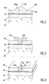
- the inlet microguide 12 can be formed by making two openings 52 and 54 in the surface layer 10 of the optical guide, the silica 10a remaining between the two openings 52 and 54 then constituting the inlet microguide.
- the openings 52 and 54 can be produced by reactive ion etching using a plasma of carbon tetrafluoride or trifluoromethane as an attack agent. This anisotropic etching is carried out over the entire thickness of the silica layer 10.
- the optical guide as shown in FIG. 2 by depositing above the silica pad 10a and the openings 52 and 54 a dielectric 56 having a refractive index lower than that of pure silica such as MgF2 .
- the microguide input as shown in FIG. 3.
- reactive ion etching of the surface layer 10 of the optical guide is carried out, over the entire thickness of the layer 10, in order to form an opening 58 which has just been fill with a dielectric 60 having a refractive index higher than that of the silica constituting the layer 10, for example alumina.
- the dimensions of the microguide are defined by the dimensions of the opening 58, while in the embodiments shown in Figures 1 and 2, the dimensions of the microguide are determined by the remaining silica pad 10a.
- the collimating lens 18 can be produced, as shown in FIG. 1, by a simple anisotropic etching of the surface layer 10, the dimensions and the shape of the opening 19 made in the silica layer 10, defining the dimensions and the optical properties of the lens.
- reactive ion etching is used using as an attack agent a trifluoromethane plasma, produced over a thickness of a few nanometers, then the etching is ended by a chemical attack in a mixture of HF-FNH4, a solution which does not attack the silicon nitride constituting the guiding layer 8 and which makes it possible to obtain very good control of the local modification of the effective index of the guide 2.
- This etching is carried out in a conventional manner, through an etching mask defining the shape and the exact dimensions of the lens 18 to be produced.
- the opening 19 made in the layer 10 and defining the dimensions of the lens 18, can be filled with a dielectric 62 having a refractive index lower than that of silica such as MgF2.
- a simple etching of the silica to form the lens 18 in order to obtain a more significant difference in the effective index of the guide (taking account of the differences in index between the air and the silica) and therefore to form diopters 18a and 18b with a small radius of curvature, which corresponds to a lens with a large aperture.
- the separating plate 22 (FIG. 1) is also produced by etching, by reactive ion etching, the layer of silica 10, with CHF3.
- ⁇ l Arsin (n e2 / n e1 ), where n e1 represents the effective index of the guide SiO2 / Si3N4 / SiO2 and n e2 represents the effective index of the air guide / Si3N4 / SiO2. This approach is only valid if n e1 -n e2 is greater than zero.
- the width of the separating blade 22 is calculated using a conventional optical calculation where the effective indices replace the real indices.
- e may for example be of the order of 2.5 ⁇ m for an angle of ⁇ l close to 78 °.
- the separating plate in the form of a diffraction grating 64, as shown in FIG. 5 operating in Bragg regime.
- the transmission and reflection coefficients of the network 64 are calculated by limiting the number of lines 66 of this network; a transmission and reflection coefficient equal to 50% is obtained using a network comprising 10 to 20 lines.
- This network can be produced by locally etching, through an appropriate etching mask obtained according to conventional photolithography methods, the silica layer 10 of the optical guide. This etching is performed anisotropically by a reactive ion etching process.
- a diffraction grating makes it possible to obtain angles ⁇ of the incident beam 20 relative to the normal N ⁇ to the lines of the grating, more distant from ⁇ / 2 than in the case of a separating plate formed by a single groove ( Figure 1).
- the network is less sensitive to any over-etching or under-etching of the silica layer 10.
- it is much more sensitive to the wavelength ⁇ 0 of the incident beam 20 than is the use of '' a single furrow.
- the diffraction grating 64 work at an order greater than 1 and for example at the order 3 or 5. This makes it possible to increase the pitch of the grating by 3 or 5 times for the same angle ⁇ and therefore to facilitate its realization: for a network working at order 1, there is a step of approximately 600 nm and for a network working at order 3, there is a step of 1800 nm.
- the angle ⁇ can be less than 78 °, leading to a smaller footprint than the single groove ( Figure 1).
- it must necessarily be greater than a limit angle ⁇ in order not to have energy loss by diffraction by the lower orders of the network.
- the phase shifter 28 is also produced, as shown in FIG. 1, by a simple groove etched in the surface layer 10 of the optical guide and over its entire thickness.
- L is typically of the order a few micrometers for a phase shifter formed by a simple etching of the layer 10.
- the mirrors 30 and 36 can be produced, as shown in FIGS. 6a and 6b, by a complete etching of the optical guide 2, up to the substrate.
- This etching is preferably carried out by reactive ion etching using as an attack agent CF4, CHF3, C2F4 or SF6 for layers of silica and silicon nitride, in order to obtain etched sides 68 perfectly anisotropic.
- a layer 72 can then be deposited on the entire guide improving in particular the properties of the microguide 12 and ensuring mechanical protection of the mirrors.
- This layer 72 can be pure silica deposited by CVD, a polyimide or a silica gel known under the name of "Spin on glass".
- the various components can be produced by etching this dielectric layer.
Landscapes
- Physics & Mathematics (AREA)
- General Physics & Mathematics (AREA)
- Engineering & Computer Science (AREA)
- Microelectronics & Electronic Packaging (AREA)
- Optics & Photonics (AREA)
- Instruments For Measurement Of Length By Optical Means (AREA)
- Optical Integrated Circuits (AREA)
Applications Claiming Priority (2)
| Application Number | Priority Date | Filing Date | Title |
|---|---|---|---|
| FR8704877 | 1987-04-07 | ||
| FR8704877A FR2613826B1 (fr) | 1987-04-07 | 1987-04-07 | Capteur de deplacement en optique integree |
Publications (2)
| Publication Number | Publication Date |
|---|---|
| EP0286528A1 true EP0286528A1 (de) | 1988-10-12 |
| EP0286528B1 EP0286528B1 (de) | 1991-06-26 |
Family
ID=9349875
Family Applications (1)
| Application Number | Title | Priority Date | Filing Date |
|---|---|---|---|
| EP88400814A Expired - Lifetime EP0286528B1 (de) | 1987-04-07 | 1988-04-05 | Optisch integrierter Verschiebungssensor |
Country Status (6)
| Country | Link |
|---|---|
| US (1) | US4865453A (de) |
| EP (1) | EP0286528B1 (de) |
| JP (1) | JPS63262504A (de) |
| CA (1) | CA1295713C (de) |
| DE (1) | DE3863382D1 (de) |
| FR (1) | FR2613826B1 (de) |
Cited By (11)
| Publication number | Priority date | Publication date | Assignee | Title |
|---|---|---|---|---|
| EP0367675A1 (de) * | 1988-11-04 | 1990-05-09 | Commissariat A L'energie Atomique | Integrierte Optikvorrichtung zur Messung des Brechungsindex einer Flüssigkeit |
| FR2660440A1 (fr) * | 1990-04-03 | 1991-10-04 | Commissariat Energie Atomique | Composant optique integre protege contre l'environnement et son procede de fabrication. |
| EP0452938A3 (en) * | 1990-04-20 | 1992-04-15 | Japan Aviation Electronics Industry, Limited | Optical integrated circuit |
| WO1992006353A1 (de) * | 1990-10-01 | 1992-04-16 | Tabarelli, Werner | Interferometer |
| EP0509716A1 (de) * | 1991-04-10 | 1992-10-21 | Canon Kabushiki Kaisha | Kantilevereinheit, und Atomkraftmikroskop, Magnetkraftmikroskop, Wiedergabe- und Informationsverarbeitungsapparat mit solcher Kantilevereinheit |
| EP0541247A1 (de) * | 1991-10-16 | 1993-05-12 | AT&T Corp. | Optische integrierte Schaltung |
| FR2685096A1 (fr) * | 1991-12-16 | 1993-06-18 | Commissariat Energie Atomique | Miroir optique integre et son procede de fabrication. |
| FR2687472A1 (fr) * | 1992-02-15 | 1993-08-20 | Daimler Benz Ag | Interferometre optique integre pour mesure d'allongement. |
| US5261014A (en) * | 1991-09-06 | 1993-11-09 | France Telecom Etablissement Autonome De Droit Public | Optoelectronic device with integrated optical guide and photo-detector. |
| FR2699269A1 (fr) * | 1992-12-10 | 1994-06-17 | Merlin Gerin | Dispositif de mesure interferrométrique. |
| FR2699270A1 (fr) * | 1992-12-10 | 1994-06-17 | Merlin Gerin | Capteur optique intégré pour la détection de la variation de chemin optique d'un faisceau lumineux. |
Families Citing this family (20)
| Publication number | Priority date | Publication date | Assignee | Title |
|---|---|---|---|---|
| DE3932663A1 (de) * | 1989-09-29 | 1991-04-18 | Hommelwerke Gmbh | Stehende-wellen-sensor |
| ATE105402T1 (de) * | 1989-12-23 | 1994-05-15 | Heidenhain Gmbh Dr Johannes | Positionsmesseinrichtung. |
| EP0468019B1 (de) * | 1990-02-09 | 1994-07-06 | Dr. Johannes Heidenhain GmbH | Interferometer |
| DE59008904D1 (de) * | 1990-06-07 | 1995-05-18 | Litef Gmbh | Integrierte optische Einrichtung zur interferometrischen Vermessung von Lichtwellen. |
| US5239183A (en) * | 1991-04-30 | 1993-08-24 | Dainippon Screen Mfg. Co., Ltd. | Optical gap measuring device using frustrated internal reflection |
| FR2676808B1 (fr) * | 1991-05-21 | 1993-08-13 | Commissariat Energie Atomique | Dispositif de mesure d'une caracteristique d'un objet en optique integree, par interferometrie. |
| US5253319A (en) * | 1992-02-24 | 1993-10-12 | Corning Incorporated | Planar optical waveguides with planar optical elements |
| DE4230087A1 (de) * | 1992-09-09 | 1994-03-10 | Bezzaoui Hocine Dipl Ing | Integrierte optisch/mikromechanische Sensoren |
| JP2802868B2 (ja) * | 1992-12-22 | 1998-09-24 | 大日本スクリーン製造株式会社 | 半導体ウエハの非接触電気測定用センサおよびその製造方法、並びに、そのセンサを用いた測定方法 |
| JPH06349920A (ja) * | 1993-06-08 | 1994-12-22 | Dainippon Screen Mfg Co Ltd | 半導体ウェハの電荷量測定方法 |
| US5493437A (en) * | 1993-09-13 | 1996-02-20 | Motorola | External communication link for a credit card pager |
| GB9320500D0 (en) * | 1993-10-05 | 1993-11-24 | Rensihaw Plc | Interferometric distance measuring apparatus |
| FR2748573B1 (fr) * | 1996-05-10 | 1998-06-05 | Commissariat Energie Atomique | Filtre en optique integree |
| EP1506440A4 (de) * | 2002-05-17 | 2005-08-10 | Nanoventions Inc | Planarer optischer wellenleiter |
| GB0222970D0 (en) * | 2002-10-04 | 2002-11-13 | Renishaw Plc | Vacuum compatible laser interferometer |
| WO2012162809A1 (en) * | 2011-05-31 | 2012-12-06 | Tornado Medical Systems, Inc. | Interferometery on a planar substrate |
| CN103900603B (zh) * | 2014-04-21 | 2016-05-11 | 哈尔滨工业大学 | 平面或曲面内无导轨二维运动物体的位移和姿态的非接触测量方法 |
| GB2545912A (en) * | 2015-12-29 | 2017-07-05 | Nokia Technologies Oy | Interferometry |
| EP3742757B1 (de) * | 2019-05-22 | 2022-12-28 | ams International AG | Optischer wandler und verfahren zur messung einer verschiebung |
| WO2022123705A1 (ja) * | 2020-12-09 | 2022-06-16 | 日本電信電話株式会社 | 光センサ |
Citations (2)
| Publication number | Priority date | Publication date | Assignee | Title |
|---|---|---|---|---|
| US4324492A (en) * | 1978-06-01 | 1982-04-13 | Drenckhan Juergen | Method of and arrangement for performing optical interference measurements |
| EP0198735A1 (de) * | 1985-03-15 | 1986-10-22 | Commissariat A L'energie Atomique | Optoelektronischer Wandler und Verfahren zu seiner Herstellung |
Family Cites Families (2)
| Publication number | Priority date | Publication date | Assignee | Title |
|---|---|---|---|---|
| DE3630887A1 (de) * | 1986-03-26 | 1987-10-08 | Hommelwerke Gmbh | Vorrichtung zur messung kleiner laengen |
| EP0242407A2 (de) * | 1986-03-26 | 1987-10-28 | Hommelwerke GmbH | Vorrichtung zur Messung kleiner Längen |
-
1987
- 1987-04-07 FR FR8704877A patent/FR2613826B1/fr not_active Expired - Lifetime
-
1988
- 1988-03-29 US US07/174,827 patent/US4865453A/en not_active Expired - Fee Related
- 1988-04-05 EP EP88400814A patent/EP0286528B1/de not_active Expired - Lifetime
- 1988-04-05 DE DE8888400814T patent/DE3863382D1/de not_active Expired - Lifetime
- 1988-04-06 CA CA000563412A patent/CA1295713C/en not_active Expired - Lifetime
- 1988-04-07 JP JP63086233A patent/JPS63262504A/ja active Pending
Patent Citations (2)
| Publication number | Priority date | Publication date | Assignee | Title |
|---|---|---|---|---|
| US4324492A (en) * | 1978-06-01 | 1982-04-13 | Drenckhan Juergen | Method of and arrangement for performing optical interference measurements |
| EP0198735A1 (de) * | 1985-03-15 | 1986-10-22 | Commissariat A L'energie Atomique | Optoelektronischer Wandler und Verfahren zu seiner Herstellung |
Non-Patent Citations (1)
| Title |
|---|
| TECHNISCHES MESSEN TM, vol. 52, no. 9, 1985, pages 321-326, Munich, DE; H.-J. BOEHNEL et al.: "Miniaturisiertes Halbleiterlaser-Interferometer für die industrielle Wegmessung" * |
Cited By (20)
| Publication number | Priority date | Publication date | Assignee | Title |
|---|---|---|---|---|
| FR2638847A1 (fr) * | 1988-11-04 | 1990-05-11 | Commissariat Energie Atomique | Dispositif optique integre pour la mesure d'indice de refraction d'un fluide |
| US5073024A (en) * | 1988-11-04 | 1991-12-17 | Commissariat A L'energie Atomique | Integrated optical device for measuring the refractive index of a fluid |
| EP0367675A1 (de) * | 1988-11-04 | 1990-05-09 | Commissariat A L'energie Atomique | Integrierte Optikvorrichtung zur Messung des Brechungsindex einer Flüssigkeit |
| US5210801A (en) * | 1990-04-03 | 1993-05-11 | Commissariat A L'energie Atomique | Environmentally protected integrated optical component and its production process |
| FR2660440A1 (fr) * | 1990-04-03 | 1991-10-04 | Commissariat Energie Atomique | Composant optique integre protege contre l'environnement et son procede de fabrication. |
| EP0451047A1 (de) * | 1990-04-03 | 1991-10-09 | Commissariat A L'energie Atomique | Vor Umwelteinflüssen geschützte integrierte optische Komponente und Verfahren zu ihrer Herstellung |
| EP0452938A3 (en) * | 1990-04-20 | 1992-04-15 | Japan Aviation Electronics Industry, Limited | Optical integrated circuit |
| WO1992006353A1 (de) * | 1990-10-01 | 1992-04-16 | Tabarelli, Werner | Interferometer |
| EP0509716A1 (de) * | 1991-04-10 | 1992-10-21 | Canon Kabushiki Kaisha | Kantilevereinheit, und Atomkraftmikroskop, Magnetkraftmikroskop, Wiedergabe- und Informationsverarbeitungsapparat mit solcher Kantilevereinheit |
| EP0791803A3 (de) * | 1991-04-10 | 1997-10-22 | Canon Kk | Cantilevereinheit und Atomkraftmikroskop, Magnetkraftmikroskop, sowie Wiedergabe- und Informationsverarbeitungsapparat damit |
| US5260567A (en) * | 1991-04-10 | 1993-11-09 | Canon Kabushiki Kaisha | Cantilever unit and atomic force microscope, magnetic force microscope, reproducing apparatus and information processing apparatus using the cantilever unit |
| US5261014A (en) * | 1991-09-06 | 1993-11-09 | France Telecom Etablissement Autonome De Droit Public | Optoelectronic device with integrated optical guide and photo-detector. |
| EP0541247A1 (de) * | 1991-10-16 | 1993-05-12 | AT&T Corp. | Optische integrierte Schaltung |
| FR2685096A1 (fr) * | 1991-12-16 | 1993-06-18 | Commissariat Energie Atomique | Miroir optique integre et son procede de fabrication. |
| EP0547955A1 (de) * | 1991-12-16 | 1993-06-23 | Commissariat A L'energie Atomique | Integriert-optischer Spiegel und Verfahren zu seiner Herstellung |
| FR2687472A1 (fr) * | 1992-02-15 | 1993-08-20 | Daimler Benz Ag | Interferometre optique integre pour mesure d'allongement. |
| FR2699269A1 (fr) * | 1992-12-10 | 1994-06-17 | Merlin Gerin | Dispositif de mesure interferrométrique. |
| FR2699270A1 (fr) * | 1992-12-10 | 1994-06-17 | Merlin Gerin | Capteur optique intégré pour la détection de la variation de chemin optique d'un faisceau lumineux. |
| WO1994014028A1 (fr) * | 1992-12-10 | 1994-06-23 | Merlin Gerin | Dispositif de mesure interferometrique |
| US5710629A (en) * | 1992-12-10 | 1998-01-20 | Schneider Electric S.A. | Interferometric measuring device forming a spacial interference pattern |
Also Published As
| Publication number | Publication date |
|---|---|
| US4865453A (en) | 1989-09-12 |
| CA1295713C (en) | 1992-02-11 |
| DE3863382D1 (de) | 1991-08-01 |
| FR2613826B1 (fr) | 1990-10-26 |
| JPS63262504A (ja) | 1988-10-28 |
| FR2613826A1 (fr) | 1988-10-14 |
| EP0286528B1 (de) | 1991-06-26 |
Similar Documents
| Publication | Publication Date | Title |
|---|---|---|
| EP0286528B1 (de) | Optisch integrierter Verschiebungssensor | |
| EP0367675B1 (de) | Integrierte Optikvorrichtung zur Messung des Brechungsindex einer Flüssigkeit | |
| EP0006052B1 (de) | Kompakte optische Struktur mit eingebauter Quelle | |
| EP0451047B1 (de) | Vor Umwelteinflüssen geschützte integrierte optische Komponente und Verfahren zu ihrer Herstellung | |
| EP0584005B1 (de) | Integrierter optischer Sensor, insbesondere für chemische Substanzen | |
| EP0270429B1 (de) | Optisch integrierter Lesekopf zum Auslesen von auf einem magnetischen Träger aufgezeichneten Informationen | |
| EP0033048B1 (de) | Interferometer mit abstimmbarer optischer Höhlung, das eine optische monomoden Faser befasst, und dessen Anwendung zur Filtrierung und Spektrographie | |
| EP0506546A2 (de) | Optischer Faser mit Bragg-Gitter und ihre Anwendungen | |
| FR2570839A1 (fr) | Dispositif de couplage entre des guides d'onde, monolithiquement integre avec ceux-ci sur un substrat semiconducteur | |
| EP0647311B1 (de) | Völlig integrierter optischer kreisel von sagnac typ | |
| EP4016053A1 (de) | Optische komponente für eine interferometrische bildgebungsvorrichtung | |
| EP0971203A1 (de) | Verfahren und Vorrichtung zur Messung der Dicke von transparenten Materialien | |
| CH684212A5 (fr) | Dispositif optique à interférométrie en lumière blanche. | |
| EP0585333B1 (de) | Optisch integrierte, interferometrische messvorrichtung | |
| FR3052923A1 (fr) | Reflecteur optique resonant a multiples couches minces de materiaux dielectriques, capteur optique et dispositif d'amplification laser comportant un tel reflecteur | |
| EP0448415B1 (de) | Abstandsdetektionsanordnung einer physikalischen Grösse durch Reflektion | |
| WO1999064905A1 (fr) | Dispositif de diffraction de lumiere enfoui dans un materiau | |
| FR3064375A1 (fr) | Dispositif a capteur optique utilisant une onde optique de surface couplee par un reseau de diffraction | |
| FR2719387A1 (fr) | Dispositif de contrôle de la position et/ou de la focalisation d'un faisceau lumineux focalisé. | |
| WO2020225513A1 (fr) | Dispositif de répartition de signal pour la mesure de décalages en longueur d'onde | |
| EP0591912B1 (de) | Interferometer, bestehend aus einer integrierten Anordnung und einem Spiegel, die durch eine Messzone voneinander getrennt sind | |
| EP0433240A2 (de) | Optische hochwirksame Wandlerzelle und deren Anwendung bei optischen Sensoren | |
| EP0499545A1 (de) | Empfänger zum paralellen Demultiplexen für ein optisches Sensornetzwerk mit Spektralmodulationskodierung | |
| FR2778458A1 (fr) | Dispositif optique de mesure interferometrique d'un deplacement relatif entre deux elements dont l'un au moins est mobile relativement a l'autre | |
| FR3052913A1 (fr) | Capteur optique comportant un reflecteur optique resonant a multiples couches minces de materiaux dielectriques |
Legal Events
| Date | Code | Title | Description |
|---|---|---|---|
| PUAI | Public reference made under article 153(3) epc to a published international application that has entered the european phase |
Free format text: ORIGINAL CODE: 0009012 |
|
| AK | Designated contracting states |
Kind code of ref document: A1 Designated state(s): CH DE GB IT LI NL |
|
| 17P | Request for examination filed |
Effective date: 19890316 |
|
| 17Q | First examination report despatched |
Effective date: 19900716 |
|
| GRAA | (expected) grant |
Free format text: ORIGINAL CODE: 0009210 |
|
| AK | Designated contracting states |
Kind code of ref document: B1 Designated state(s): CH DE GB IT LI NL |
|
| REF | Corresponds to: |
Ref document number: 3863382 Country of ref document: DE Date of ref document: 19910801 |
|
| ITF | It: translation for a ep patent filed | ||
| GBT | Gb: translation of ep patent filed (gb section 77(6)(a)/1977) | ||
| PLBE | No opposition filed within time limit |
Free format text: ORIGINAL CODE: 0009261 |
|
| STAA | Information on the status of an ep patent application or granted ep patent |
Free format text: STATUS: NO OPPOSITION FILED WITHIN TIME LIMIT |
|
| 26N | No opposition filed | ||
| PGFP | Annual fee paid to national office [announced via postgrant information from national office to epo] |
Ref country code: CH Payment date: 19970418 Year of fee payment: 10 |
|
| PGFP | Annual fee paid to national office [announced via postgrant information from national office to epo] |
Ref country code: NL Payment date: 19970425 Year of fee payment: 10 |
|
| PG25 | Lapsed in a contracting state [announced via postgrant information from national office to epo] |
Ref country code: LI Free format text: LAPSE BECAUSE OF NON-PAYMENT OF DUE FEES Effective date: 19980430 Ref country code: CH Free format text: LAPSE BECAUSE OF NON-PAYMENT OF DUE FEES Effective date: 19980430 |
|
| PG25 | Lapsed in a contracting state [announced via postgrant information from national office to epo] |
Ref country code: NL Free format text: LAPSE BECAUSE OF NON-PAYMENT OF DUE FEES Effective date: 19981101 |
|
| REG | Reference to a national code |
Ref country code: CH Ref legal event code: PL |
|
| NLV4 | Nl: lapsed or anulled due to non-payment of the annual fee |
Effective date: 19981101 |
|
| PGFP | Annual fee paid to national office [announced via postgrant information from national office to epo] |
Ref country code: GB Payment date: 19990329 Year of fee payment: 12 |
|
| PGFP | Annual fee paid to national office [announced via postgrant information from national office to epo] |
Ref country code: DE Payment date: 19990503 Year of fee payment: 12 |
|
| PG25 | Lapsed in a contracting state [announced via postgrant information from national office to epo] |
Ref country code: GB Free format text: LAPSE BECAUSE OF NON-PAYMENT OF DUE FEES Effective date: 20000405 |
|
| GBPC | Gb: european patent ceased through non-payment of renewal fee |
Effective date: 20000405 |
|
| PG25 | Lapsed in a contracting state [announced via postgrant information from national office to epo] |
Ref country code: DE Free format text: LAPSE BECAUSE OF NON-PAYMENT OF DUE FEES Effective date: 20010201 |
|
| PG25 | Lapsed in a contracting state [announced via postgrant information from national office to epo] |
Ref country code: IT Free format text: LAPSE BECAUSE OF NON-PAYMENT OF DUE FEES;WARNING: LAPSES OF ITALIAN PATENTS WITH EFFECTIVE DATE BEFORE 2007 MAY HAVE OCCURRED AT ANY TIME BEFORE 2007. THE CORRECT EFFECTIVE DATE MAY BE DIFFERENT FROM THE ONE RECORDED. Effective date: 20050405 |