EP0286829A2 - Dispositif électronique comportant une couche de polyimide et son procédé de fabrication - Google Patents
Dispositif électronique comportant une couche de polyimide et son procédé de fabrication Download PDFInfo
- Publication number
- EP0286829A2 EP0286829A2 EP88103647A EP88103647A EP0286829A2 EP 0286829 A2 EP0286829 A2 EP 0286829A2 EP 88103647 A EP88103647 A EP 88103647A EP 88103647 A EP88103647 A EP 88103647A EP 0286829 A2 EP0286829 A2 EP 0286829A2
- Authority
- EP
- European Patent Office
- Prior art keywords
- polyimide
- integer
- alkoxy
- residues
- alkyl
- Prior art date
- Legal status (The legal status is an assumption and is not a legal conclusion. Google has not performed a legal analysis and makes no representation as to the accuracy of the status listed.)
- Withdrawn
Links
- 0 CC(*)(C(*)(C(NC)=O)[Al](C)C)C(O)=O Chemical compound CC(*)(C(*)(C(NC)=O)[Al](C)C)C(O)=O 0.000 description 2
- FLHKPCPBFXYADQ-UHFFFAOYSA-N CC(CC(CC1)c(cc2C)ccc2N)C1N Chemical compound CC(CC(CC1)c(cc2C)ccc2N)C1N FLHKPCPBFXYADQ-UHFFFAOYSA-N 0.000 description 1
- NNNYSIPLRUCYSA-UHFFFAOYSA-L CC(N[Al](C)I)=O Chemical compound CC(N[Al](C)I)=O NNNYSIPLRUCYSA-UHFFFAOYSA-L 0.000 description 1
- CBCKQZAAMUWICA-UHFFFAOYSA-N Nc(cc1)ccc1N Chemical compound Nc(cc1)ccc1N CBCKQZAAMUWICA-UHFFFAOYSA-N 0.000 description 1
- KZKRMRXXJVGHKE-UHFFFAOYSA-N Nc(cc1)ccc1OC(C=C1)=CCC1=N Chemical compound Nc(cc1)ccc1OC(C=C1)=CCC1=N KZKRMRXXJVGHKE-UHFFFAOYSA-N 0.000 description 1
Images

Classifications
-
- H—ELECTRICITY
- H10—SEMICONDUCTOR DEVICES; ELECTRIC SOLID-STATE DEVICES NOT OTHERWISE PROVIDED FOR
- H10P—GENERIC PROCESSES OR APPARATUS FOR THE MANUFACTURE OR TREATMENT OF DEVICES COVERED BY CLASS H10
- H10P14/00—Formation of materials, e.g. in the shape of layers or pillars
- H10P14/60—Formation of materials, e.g. in the shape of layers or pillars of insulating materials
- H10P14/68—Organic materials, e.g. photoresists
- H10P14/683—Organic materials, e.g. photoresists carbon-based polymeric organic materials, e.g. polyimides, poly cyclobutene or PVC
-
- G—PHYSICS
- G11—INFORMATION STORAGE
- G11B—INFORMATION STORAGE BASED ON RELATIVE MOVEMENT BETWEEN RECORD CARRIER AND TRANSDUCER
- G11B5/00—Recording by magnetisation or demagnetisation of a record carrier; Reproducing by magnetic means; Record carriers therefor
- G11B5/127—Structure or manufacture of heads, e.g. inductive
- G11B5/31—Structure or manufacture of heads, e.g. inductive using thin films
-
- G—PHYSICS
- G11—INFORMATION STORAGE
- G11B—INFORMATION STORAGE BASED ON RELATIVE MOVEMENT BETWEEN RECORD CARRIER AND TRANSDUCER
- G11B5/00—Recording by magnetisation or demagnetisation of a record carrier; Reproducing by magnetic means; Record carriers therefor
- G11B5/62—Record carriers characterised by the selection of the material
- G11B5/68—Record carriers characterised by the selection of the material comprising one or more layers of magnetisable material homogeneously mixed with a bonding agent
- G11B5/70—Record carriers characterised by the selection of the material comprising one or more layers of magnetisable material homogeneously mixed with a bonding agent on a base layer
- G11B5/702—Record carriers characterised by the selection of the material comprising one or more layers of magnetisable material homogeneously mixed with a bonding agent on a base layer characterised by the bonding agent
-
- H—ELECTRICITY
- H01—ELECTRIC ELEMENTS
- H01B—CABLES; CONDUCTORS; INSULATORS; SELECTION OF MATERIALS FOR THEIR CONDUCTIVE, INSULATING OR DIELECTRIC PROPERTIES
- H01B3/00—Insulators or insulating bodies characterised by the insulating materials; Selection of materials for their insulating or dielectric properties
- H01B3/18—Insulators or insulating bodies characterised by the insulating materials; Selection of materials for their insulating or dielectric properties mainly consisting of organic substances
- H01B3/30—Insulators or insulating bodies characterised by the insulating materials; Selection of materials for their insulating or dielectric properties mainly consisting of organic substances plastics; resins; waxes
- H01B3/303—Macromolecular compounds obtained by reactions forming a linkage containing nitrogen with or without oxygen or carbon in the main chain of the macromolecule, not provided for in groups H01B3/38 or H01B3/302
- H01B3/306—Polyimides or polyesterimides
-
- H—ELECTRICITY
- H01—ELECTRIC ELEMENTS
- H01F—MAGNETS; INDUCTANCES; TRANSFORMERS; SELECTION OF MATERIALS FOR THEIR MAGNETIC PROPERTIES
- H01F10/00—Thin magnetic films, e.g. of one-domain structure
- H01F10/26—Thin magnetic films, e.g. of one-domain structure characterised by the substrate or intermediate layers
- H01F10/30—Thin magnetic films, e.g. of one-domain structure characterised by the substrate or intermediate layers characterised by the composition of the intermediate layers, e.g. seed, buffer, template, diffusion preventing, cap layers
-
- H—ELECTRICITY
- H05—ELECTRIC TECHNIQUES NOT OTHERWISE PROVIDED FOR
- H05K—PRINTED CIRCUITS; CASINGS OR CONSTRUCTIONAL DETAILS OF ELECTRIC APPARATUS; MANUFACTURE OF ASSEMBLAGES OF ELECTRICAL COMPONENTS
- H05K1/00—Printed circuits
- H05K1/02—Details
- H05K1/03—Use of materials for the substrate
- H05K1/0313—Organic insulating material
- H05K1/032—Organic insulating material consisting of one material
- H05K1/0346—Organic insulating material consisting of one material containing N
-
- H—ELECTRICITY
- H05—ELECTRIC TECHNIQUES NOT OTHERWISE PROVIDED FOR
- H05K—PRINTED CIRCUITS; CASINGS OR CONSTRUCTIONAL DETAILS OF ELECTRIC APPARATUS; MANUFACTURE OF ASSEMBLAGES OF ELECTRICAL COMPONENTS
- H05K3/00—Apparatus or processes for manufacturing printed circuits
- H05K3/10—Apparatus or processes for manufacturing printed circuits in which conductive material is applied to the insulating support in such a manner as to form the desired conductive pattern
- H05K3/14—Apparatus or processes for manufacturing printed circuits in which conductive material is applied to the insulating support in such a manner as to form the desired conductive pattern using spraying techniques to apply the conductive material, e.g. vapour evaporation
- H05K3/16—Apparatus or processes for manufacturing printed circuits in which conductive material is applied to the insulating support in such a manner as to form the desired conductive pattern using spraying techniques to apply the conductive material, e.g. vapour evaporation by cathodic sputtering
-
- H—ELECTRICITY
- H10—SEMICONDUCTOR DEVICES; ELECTRIC SOLID-STATE DEVICES NOT OTHERWISE PROVIDED FOR
- H10W—GENERIC PACKAGES, INTERCONNECTIONS, CONNECTORS OR OTHER CONSTRUCTIONAL DETAILS OF DEVICES COVERED BY CLASS H10
- H10W20/00—Interconnections in chips, wafers or substrates
- H10W20/40—Interconnections external to wafers or substrates, e.g. back-end-of-line [BEOL] metallisations or vias connecting to gate electrodes
- H10W20/45—Interconnections external to wafers or substrates, e.g. back-end-of-line [BEOL] metallisations or vias connecting to gate electrodes characterised by their insulating parts
- H10W20/48—Insulating materials thereof
-
- H—ELECTRICITY
- H10—SEMICONDUCTOR DEVICES; ELECTRIC SOLID-STATE DEVICES NOT OTHERWISE PROVIDED FOR
- H10W—GENERIC PACKAGES, INTERCONNECTIONS, CONNECTORS OR OTHER CONSTRUCTIONAL DETAILS OF DEVICES COVERED BY CLASS H10
- H10W70/00—Package substrates; Interposers; Redistribution layers [RDL]
- H10W70/60—Insulating or insulated package substrates; Interposers; Redistribution layers
- H10W70/67—Insulating or insulated package substrates; Interposers; Redistribution layers characterised by their insulating layers or insulating parts
- H10W70/69—Insulating materials thereof
-
- H—ELECTRICITY
- H10—SEMICONDUCTOR DEVICES; ELECTRIC SOLID-STATE DEVICES NOT OTHERWISE PROVIDED FOR
- H10W—GENERIC PACKAGES, INTERCONNECTIONS, CONNECTORS OR OTHER CONSTRUCTIONAL DETAILS OF DEVICES COVERED BY CLASS H10
- H10W74/00—Encapsulations, e.g. protective coatings
- H10W74/40—Encapsulations, e.g. protective coatings characterised by their materials
- H10W74/47—Encapsulations, e.g. protective coatings characterised by their materials comprising organic materials, e.g. plastics or resins
-
- H—ELECTRICITY
- H05—ELECTRIC TECHNIQUES NOT OTHERWISE PROVIDED FOR
- H05K—PRINTED CIRCUITS; CASINGS OR CONSTRUCTIONAL DETAILS OF ELECTRIC APPARATUS; MANUFACTURE OF ASSEMBLAGES OF ELECTRICAL COMPONENTS
- H05K2201/00—Indexing scheme relating to printed circuits covered by H05K1/00
- H05K2201/03—Conductive materials
- H05K2201/0332—Structure of the conductor
- H05K2201/0335—Layered conductors or foils
- H05K2201/0355—Metal foils
Definitions
- the present invention relates to electronic devices and particularly, it is concerned with electronic devices having interlaminar insulating films which exhibit high flatness and superior adhesive properties and with a method for producing such electronic devices.
- the technique of multilayer wiring has become indispensable to LSI's.
- Interlaminar insulation films in multilayer circuit devices are required to have insulation resistance sufficient to secure the insulation between wirings supported severally by two layers lying one over another. These insulation films are also required to have such high flatness as not to cause any fatal obstacle, such as notable level difference or break, to the productivity or reliability when the next layer wiring is fabricated.
- the insulating films are asked to exhibit superior adhesion to substrates, wirings, or other insulating films in view of the moisture resistance, durability, and reliability of the product multilayer circuit devices.
- interlaminar insulating films are investigated in both the aspects of organic and inorganic materials, organic materials are advantageous in film flatness.
- a typical example of the interlaminar organic insulating films heretofore disclosed is formed from PIQ of Hitachi Chemical Co., Ltd.
- PIQ is a varnish which provides a polyimide resin on thermal curing or chemical treatment.
- the resulting insulating films are excellent in heat resistance and mechanical properties.
- PIQ is applied on wafers by a suitable method such as spin coating and then subjected to heat treatment or some other treatment, providing intended interlaminar insulating films.
- the obtained films are superior in flatness to inorganic insulating film formed by CVD or the like. Nevertheless, a further improvement of the flatness has been required, as LSI's have become more highly integrated and accordingly have become finer in structure and higher in wiring aspect ratio. Thus, the flatness has been an important problem in LSI production processes.
- Reactive terminal groups hitherto investigated include half-esterified acid anhydride groups, ethynyl group, vinyl group, and biphenyl group.
- Japanese Patent Application Laid-Open No. 120723 proposes an electronic device comprising an insulating film(s) formed from a polymerizable oligomer having a vinyl group or an ethynyl group at an end of the molecule, by curing to polymerize. Any of these insulating films, however, is not comparable in insulating film characteristics to that of the present invention.
- the insulating film is required to exhibit sufficient bond strength to substrates, wirings, and further to other insulating films.
- the bond strength has great influence on the reliability of product and hence is an important matter.
- the adhesive property has great significance also to the production process. It is known that the adhesion between two materials is much due to polar groups present in their molecules. Therefore, the adhesive property of polyimide has been improved up to now by copolymerizing 1,3-bis( ⁇ -aminopropyl)tetramethyldisiloxane or the like having polar groups. But, the resulting film is not comparable in adhesive properties to that of the present invention.
- LSI devices it is desired for a plurality of materials forming a composite to have nearly the same coefficient of thermal expansion.
- LSI devices are compricate combinations of fine members, which are additionally exposed to high temperatures in the fabrication process and their mounting operations.
- Organic compounds generally have thermal expansion coefficients of about 5 ⁇ 10 ⁇ 5, which are 10 times and more those of inorganic compounds.
- thermal expansion coefficients of about 5 ⁇ 10 ⁇ 5, which are 10 times and more those of inorganic compounds.
- insulating films having an exceptionally low coefficient of thermal expansion equivalent to those of inorganic compounds can be formed from PIQ-L100 of Hitachi Chemical Co., Ltd. But, with respect to flatness, insulating films from PIQ-L100 are similar to those from conventional PIQ and hence dissimilar to the insulating film of the present invention.
- Binders used today for the magnetic members of magnetic disks are made of epoxy-phenol resins.
- the thermal expansion coefficient of these epoxy-phenol resins is of the same order as those of common organic substances.
- PIQ-L100 in a concentration of the same order, viz some dozen % by weight, as those of currently used binders, the viscosity of PIQ-L100 in such a concentration is too high and the workability thereof is therefore markedly worse.
- Varnishes are now used for various electronic devices in their fabrication processes. Such electronic devices include ⁇ -ray shield films, flexible print substrates and semiconductor passivation films, besides the above-mentioned LSI's, thin-film magnetic heads, magnetic bubble devices, etc., wherein the flatness of films formed from varnishes is regarded as an important matter. Concentrations of varnishes used for the fabrication of these devices are generally as low as some dozen % by weight. As stated above, this is because there has been no varnish that can be applied in high concentrations and on curing, provides films having satisfactory properties.
- Insulating films formed from all polyamic acid above-mentioned polyamic acid varnish cannot satisfy the required flatness and hence have the matter when applied to electronic devices.
- the roughness of the insulating film which insulates a coil from another coil and the coils from an upper magnetic member should not exceed 0.2 m ⁇ on the film-magnetic member interface.
- the above flatness requirement can be satisfied by applying a thick coat of the varnish.
- such a thick coat of varnish is undesirable with respect to the performance since the coat results in an increased distance between the coil and the upper magnetic member.
- the desired end is achieved for the present by etching the flattened surface of such thick coats to reduce the thickness.
- the etching rate at present is not necessarily stable and is not even-throughout the coat, in either the dry process or the wet process. It has become a significant problem to involve such an etching step in the fabrication process.
- the level difference between the conductor pattern and its supporting layer if transferred as such on the Permalloy pattern, will result in unnecessary magnetic poles at the level difference portion of the Permalloy pattern and these magnetic poles will have adverse effect on the transmission of bubbles. Therefore, the level difference has been decreased by using a polyamic acid such as PIQ.
- the flatness is improved to a large extent but problems arise in mechanical and thermal properties of the formed film.
- an oligoamic acid having a terminal group of half-exterified acid anhydride an imide is produced by heat treatment, but this imide has a low molecular weight and is hence brittle.
- an imide or isoimide oligomer having a vinyl or thynyl terminal group is used, the cured polymer has markedly-inferior mechanical properties and additionally contains thermally-unstable groups such as unreacted vinyl groups and alkyl carbon-carbon single bonds.
- Adhesion of each parts is important for electronic devices of composite structure, such as LSI's and high-density circuit boards.
- polyimide resin in use today are not necessarily sufficient in adhesive properties, hence detracting the moisture-proof reliability of products. This is conceivably because the polyimide skeleton has a strong cohesive force and contains no hydroxy or carboxy group in a state capable of forming a hydrogen bond with other substances.
- a polar group-containing monomer such as 1,3-bis( ⁇ -aminopropyl)-tetramethylsiloxane has been copolymerized up to now.
- gate, source, drain and wiring in LSI, coil, magnetic body and wiring in a magnetic head, and conductor, permalloy, in a bubble memory etc. correspond to it.
- the first feature of the invention is that, in an electronic device having a polyimide layer which is in direct or indirect contact with at least one active area of the electronic device, the main chain of the polyimide is constituted of all or some of the residues: (wherein, R is selected from the group consisting of alkyl, fluorinated alkyl, alkoxy, fluorinated alkoxy, acyl, and halogen, l is an integer of 0 to 4, m is an integer of 0 to 3 and n is an integer of 0 to 2, and the polyimide has, at one end of the molecule, a carboxy group attached to an aliphatic carbon atom.
- the second feature of the invention is that in an electronic device having an insulating layer formed of a polyimide between conductors or semiconductors, the main chain of the polyimide is constituted of all or some of the residues of the above formulae (1) to (5), the polyimide has, at one end of the molecule, a carboxy group attached to an aliphatic carbon atom, and the insulating layer is formed between a silicon wafer and a wiring or between wirings.
- the third feature of the invention is that in a thin-film magnetic head having an insulating layer between a substrate and a wiring or between wirings, the insulating layer is formed of a polyimide, the main chain of the polyimide is constituted of all or some of the residues of the above formulae (1) to (5), and the polyimide has, at one end of the molecule, a carboxy group attached to an aliphatic carbon atom.
- the forth feature of the invention is that in a high-density circuit board having an insulating layer between a substrate and a wiring or between wirings, the insulating layer is formed of a polyimide, the main chain of the polyimide is constituted of all or some of the residue of the above formulae (1) to (5), and the polyimide has, at one end of the molecule, a carboxy group attached to an aliphatic carbon atom.
- the fifth feature of the invention is that in a magnetic bubble memory having an insulating layer between a substrate and a wiring or between wirings, the insulating layer is formed of a polyimide, the main chain of the polyimide is constituted of all or some of the residues of the above formulae (1) to (5), and the polyimide has, at one end of the molecule, a carboxy group attached to an aliphatic carbon atom.
- the sixth feature of the invention is that in a magnetic disk comprising a magnetic material-containing insulating layer formed on a nonmagnetic substrate, the insulating layer is formed of a polyimide, the main chain of the polyimide is constituted of all or some of the residues of the above formulae (1) to (5), and the polyimide has, at one end of the molecule, a carboxy group attached to an aliphatic carbon atom.
- the seventh feature of the invention is that in a solar battery comprising a substrate coated with an insulating layer, the insulating layer is formed of a polyimide, the main chain of the polyimide is constituted of all or some of the residues of the above formulae (1) to (5), and the polyimide has, at one end of the molecule, a carboxy group attached to an aliphatic carbon atom.
- the eighth feature of the invention is that in a memory device having an insulating layer as an ⁇ -ray shield film between conductors or semiconductors, the insulating layer is formed of a polyimide, the main chain of the polyimide is constituted of all or some of the residues of the above formulae (1) to (5), and the polyimide has, at one end of the molecule, a carboxy group attached to an aliphatic carbon atom.
- the nineth feature of the invention is that in an electronic device having a polyimide layer being in direct or indirect contact with at least one active area of the electronic device, the polyimide layer is formed of a product of reacting the following compounds I and II: with each other, where the n of compound I and the n ⁇ of compound II are each an integer of 0 to 10, the n ⁇ of compound I is an integer of 2 to 12, and Ar and Ar ⁇ are aromatic residues.
- One end of the molecule of compound I need not take imido structure and may take acid anhydride structure.
- the tenth feature of the invention is that in compounds I and II, Ar is selected from the following residues. and Ar ⁇ is selected from the following residues: (in residues III to IX, R is selected from the group consisting of alkyl, fluorinated alkyl, alkoxy, fluorinated alkoxy, acyl, and halogen, l in residue III is an integer of 0 to 2 and l in residues VII, VIII and IX is an integer of 0 to 4, m is an integer of 0 to 3, and n is an integer of 0 to 4).
- Suitable aromatic diamines for use in the invention include, for example, p-phenylene-diamine, 2,5-diaminotoluene, 2,5-diaminoxylene, diaminodurene (2,3,5,6-tetramethyl-p-phenylenediamine), 2,5-diaminobenzene trifluoride, 2,5-diaminoanisole, 2,5-diaminoacetophenone, 2,5-diaminobenzophenone, 2,5-diaminodiphenyl, 2,5-diaminofluorobenzene, benzidine, o-tolidine, m-tolidine, 3,3 ⁇ ,5,5 ⁇ -tetramethylbenzidine, 3,3 ⁇ -dimethoxybenzidine, 3,3 ⁇ -di(trifluoromethyl)-benzidine, 3,3 ⁇ -diacetylbenzidine, 3,3 ⁇ -difluorobenzidine, o
- Suitable tetracarboxylic cianhydride derivatives for use in the invention include, for example, pyromellitic dianhydride, methylpyromellitic dianhydride, dimethylpyromellitic dianhydride, di(trifluoromethyl)-pyromellitic dianhydride, 3,3 ⁇ ,4,4 ⁇ -biphenyltetracarboxylic dianhydride, 5,5 ⁇ -dimethyl-3,3 ⁇ ,4,4 ⁇ -biphenyltetracarboxylic dianhydride, p-(3,4-dicarboxyphenyl)-benzene, the main chains of polyimides having low thermal expansibility in particular which are useful in the invention are constituted of at least one of the following residues: wherein, R is selected from the group consisting of alkyl, fluorinated alkyl, alkoxy, fluorinated alkoxy, acyl, and halogen, l is an integer of 0 to 4, m
- R is selected from the group consisting of alkyl, fluorinated alkyl, alkoxy, fluorinated alkoxy, acyl, and halogen
- k is an integer of 0 to 3
- l is an integer of 0 to 4
- m is an integer of 0 to 3
- n is an integer of 0 to 2.
- polyimides are formed by coating polyamic acids, followed by thermal curing of the coats. From common polyamic acids, however, it is impossible to obtain any polyimide having an aliphatic carboxy group(s) at one or both ends of the molecule. Therefore terminals of polyimide molecules need to by modified by some suitable method. However, polyimides are generally insoluble in any solvent and hence it is practically impossible to convert the terminal thereof into an aliphatic carboxy group by modification. The present inventors made intensive studies for the purpose of synthesizing a polyimide having an aliphatic carboxy group at one or both ends of the molecule. As a result, it has been revealed that the following compounds I and II are best suited for use to synthesize such a polyimide.
- n and n ⁇ are each an integer of 0 to 10
- n ⁇ is an integer of 2 to 12
- Ar and Ar ⁇ denote aromatic residues.
- compounds I where n is at least 1 can be produced each by reacting an acid anhydride with a prescribed amount of lactum at a temperature of 180 to 200°C for a period of 10 to 30 hours, cooling the resulting reaction mixture to room temperature, and adding a prescribed amount of diamine.
- a varnish prepared by dissolving compounds I and II has a much lower viscosity than that of the conventional polyamic acid varnish of the same concentration. This is consistent with the general rule of the viscosity of polymer in concentrated solution, that is, the viscosity is nearly proportional to the 6th power of the molecular weight of polymer. Accordingly, a highly concentrated varnish can be prepared by dissolving compounds I and II in a solvent. Thus, it becomes possible by using this varnish to produce electronic devices provided with insulating films superior in flatness. In addition, electronic device production processes wherein this varnish is used are advantageous industrially in that the volatilization and dissipation of solvent is limited. It has been revealed that when this varnish is heated, polymerization takes place, yielding finally a polyimide whose mechanical properties and heat resistance are equivalent to those of the polyimide produced from the conventional polyamic acid.
- n ⁇ of compound I is advantageous in that the longer CH2 , group provided the higher solubility to compound I.
- CH2 chain length is increased, the diffusion of an aminocarboxylic acid formed during the varnish curing becomes slower, causing an increase in the amount of aminocarboxylic acid remaining in the product polymer. This, having adverse effects on the heat resistance and mechanical properties of polyimide, should be avoided.
- preferred values of n ⁇ are approximately from 2 to 8.
- the molar ratio of the acid dianhydride to the lactum is preferred to be from about 1:1 to about 1:3.
- Aromatic diamines :
- modified polyimides having lower permittivity and/or lower hygroscopicity have been prepared from acid dianhydrides and aromatic diamines by introducivelying, into these starting compounds, alkyl, fluorinated alkyl, alkoxy, fluorinated alkoxy, or halogen.
- a polyimide more improved in adhesive properties may be obtained by using an adhesion improver such as 1,3-bis(3,4-dicarboxy[1,2,2]bicyclo)tetramethyldisiloxane dianhydride.
- polyimides having rod-like structure exhibit low thermal expansibility. Accordingly, electronic devices provided with insulating films which are superior in flatness and have low remaining thermal stress can be produced by using a present typical starting materials for producing such polyimides.
- Aromatic diamines :
- a polyimide used herein When a polyimide used herein has rigid rod-like structure, it is readily foreseeable that the polyimide will exhibit a low thermal expansibility. Since the low thermal expansibility results from the skeletal structure of the main chain, it is also obvious that the thermal expansibility can be further lowered by introducing alkyl, fluorinated alkyl, alkoxy, fluorinated alkoxy, acyl or halogen into the aromatic ring of the monomer(s). In addition, modifications are possible by copolymerizing other diamines or acid dianhydrides.
- a flexible polyimide is produced by copolymerizing 3,3 ⁇ ,4,4 ⁇ -benzophenonetetracarboxylic acid or the like that can provide flexibility in such an amount as not to sacrifice the low thermal expansibility; the adhesive property can be more improved by copolymerizing an adhesion improver such as 1,3-bis(3,4-dicarboxy[1,2,2]bicyclo)tetramethyldisiloxane dianhydride, as stated above; and the wet etching performance characteristic, which is important for LSI fabrication processes, can be controlled by copo1ymerizing pyromellitic dianhydride, the formula of which is given above, with 3,3 ⁇ ,4,4 ⁇ -biphenyltetracarboxylic dianhydride.
- the present inventive polyimide, electronic devices and process for the production thereof are very useful for the following applications:
- the composite film when an organic coating material is applied on a metal or inorganic plate that has a very small coefficient of thermal expansion as compared with those of common organic polymers, the composite film will deform or break or the coating will develop cracks or undergo peeling on account of the thermal stress resulting from the difference in the coefficient of thermal expansion.
- the thermal stress when remarkable may cause the passivation film (protecting film) to peel off or the silicon wafer itself to cleave to destruction.
- PIQ-L100 is a varnish which, on heating or chemical treatment, provides a polyimide having a thermal expansion coefficient of about 1.0 ⁇ 10 ⁇ 6 deg ⁇ 1, which is as small as those of inorganic substances.
- this varnish is an excellent material from the viewpoint of the relaxation of thermal stress in organic-in-organic composites.
- a problem of PIQ-L100 is that the flattening property is not taken into consideration. This is explained below taking an LSI multilayer circuit device as an example.
- the interlaminar insulating film is made up in the following way: A polyimide coating 3-4 m ⁇ thick is formed on a layer having a wiring level difference of about 1 um and flattened, and then a large part of the coating thickness is etched back by oxygen RIE (Reactive Ion Etching).
- RIE reactive Ion Etching
- the speed of etch back by the RIE is not necessary uniform throughout the whole area of the coating and the end point is different to detect.
- process problems such as the contamination of the reactor and product with matter resulting from the etching. Accordingly, the etching needs to be minimized.
- a resin superior in the flattening property is strongly desired.
- electronic devices wherein thermal stress is reduced in the extreme, provided with flat insulating films which exhibit satisfactory-mechanical properties and heat resistance can be produced by using a varnish of low viscosity which contains low molecular compounds in high concentrations but, on heating provides a macromolecular imide resin exhibiting low thermal expansibility.
- varnishes in various forms are used in numerous processes for producing electronic devices. These varnishes are used in low concentrations of some dozen %.
- polyamic acids in varnish form are converted into polyimides by volatilizing the solvent and further heating or chemical treatment of the residue.
- a varnish of low concentration is used, a long time will be consumed for drying as written in Journal of Applied Polymer Science, 32 , 4541-4552 (1986) and in addition more energy will be consumed.
- Another problem is the development of voids.
- the varnish of low concentration as compared with a varnish having the same viscosity at a high concentration, loses fluidity in drying while the solvent remains in a larger amount.
- the electronic device of the present invention is provided with a homogeneous interlaminar insulating film which combines superior flatness and adhesive properties as well as excellent mechanical properties. Accordingly, the production process and the product have improved reliability and the product exhibits higher performance.
- the present inventive process for producing electronic devices employs a low-viscosity varnish comprising high-concentrations of compounds I and II which have low molecular weights but, on heating, react with each other to form a macromolecular polyimide, thereby providing electronic devices having interlaminar insulating films which combine superior flatness and adhesive properties as well as excellent mechanical properties.
- a low-viscosity varnish comprising high-concentrations of compounds I and II which have low molecular weights but, on heating, react with each other to form a macromolecular polyimide, thereby providing electronic devices having interlaminar insulating films which combine superior flatness and adhesive properties as well as excellent mechanical properties.
- the rationalization of facilities and the preservation of energy can also be achieved since the curing of the varnish requires the volatilization of less solvent.
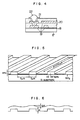
- Fig. 1 shows a cross section of the multilayer circuit portion of an LSI.
- 1 is a silicon wafer, 2 a thermally oxidized film, 3 an aluminum wiring, and 4 an insulating polyimide film of low thermal expansibility.
- This insulating film when formed by spin coating, offsets largely the level difference due to the Al wiring, thus providing a flat and highly reliable wiring structure.
- thermal stress exerted on the device is minimized because of the low thermal expansibility of the insulating film. If the thermal stress is great, cracks will develop in the device.
- the film of low thermal expansibility can be readily processed by using hydrazine or the like.
- the etching speed is about twice as high as in case of the conventional polyimide.
- the shrinkage under curing is inhibited by the silicon wafer and thus the insulating film exhibits low thermal expansibility.
- Fig. 2 is a cross-sectional view of a magnetic bubble memory device.
- 5 is a substrate made of garnet, 6 a conductor, 7 an insulating polyimide film, and 8 a Permalloy member.
- the insulating film is formed from the present inventive varnish by spin coating, the level difference due to the conductor can be offset to a great extent and transmission characteristics of the magnetic bubble device can be largely improved.
- the rise angle 9 also is much smaller than in the case of polyimides formed from conventional polyamic acids. When a present inventive polyimide of lower thermal expansibility is used, less thermal stress is exerted between the polyimide film and each of other inorganic materials.
- Fig. 3 show a cross section of a thin-film magnetic head.
- 10 is an underlying alumina layer, 11 a lower magnetic member, 12 a gap alumina, 13 the first conductor coil, 14 an interlaminar insulating polyimide film, 15 the second conductor coil, and 16 an upper magnetic member.
- the interlaminar insulating film is formed from the present inventive varnish by spin coating, the level differences due to the conductor coils can be offset to a great extent.
- a flat-surfaced insulating film has been formed by thick coating, followed by etching back. The amount of insulating layer etched can be reduced to one half by forming the present invention polyimide. Thereby, the production process can be cut largely and the accuracy of film thickness can be improved.
- Fig. 4 shows a cross section of a high-density circuit board.
- 17 is a silicon wafer, 18 a thermally oxidized film, 19 a copper wiring, 20 an interlaminar insulating polyimide film, 21 a BLM (Burried Layered Metal), and 22 a Pb/Sm electrode.
- the interlaminar insulating film is formed of the present inventive polyimide by spin coating, the level difference due to the copper wiring can be offset to a large extent and a flat, highly reliable wiring structure can be provided.
- a present inventive polyimide of low thermal expansibility is used, thermal stress in the device can be reduced extremely.
- Table 1 shows results of evaluating typical polyimides for flatness and mechanical and thermal properties, which are regarded as necessary characteristics to use in electronic devices.
- Coefficients of thermal expansion of these polyimides were measured in the following way: A sample of the varnish was applied by an application to coat uniformly a glass plate. The coating was dried at a temperature of 80 to 100°C for a period of 30 to 60 minutes to form a film. This film was peeled from the glass plate fixed on an iron frame, and heated at 200, 300 and 400°C for 60 minutes each, giving a 30-200- ⁇ m thick polyimide film. A piece (3 mm ⁇ 80 mm) was cut off from this polyimide film, interposed between two glass plates, then heated again to 500°C, and cooled gradually to remove residual strain. The dimensional change of this film with temperature below the glass transition point was measured by using.
- the flatness was evaluated by using test substrates prepared each by forming an aluminum pattern as shown in Fig. 5 on a silicon base plate. That is, a sample varnish was applied on this test substrate by spin coating and cured under the same conditions as used in the above stated preparation of thermal expansion test specimens, thereby preparing a flatness test specimen having a predetermined thickness.
- the revolution of the spinner coater was varied from 1000 to 8000 rpm depending on the necessary film thickness.
- the heat resistance is represented by the temperature at which heating of the sampler for 100 minutes resulted in 3% loss in the weight of the sample.
- the tensile strength was measured of the same test specimens as prepared in the measurement of the coefficient of thermal expansion, at room temperature by using a Thamal Mechanical Analizer.
- Table 2 shows results of testing for adhesive properties of typical polyimides.
- Polyimides 19 and 20 were obtained similarly to polyimide 18 from polyamic acids which were prepared from the same acid dianhydride and the same respective diamines as used for the preparation of polyimides 2 and 3.
- the sample tested for adhesive properties was prepared by forming a thermally oxidized film on a silicon substrate, treating the oxidized film with an aluminum chelate, applying a given varnish on the treated surface by spin coating, curing the varnish coat at 350°C to form the first polyimide layer, coarsening the surface of this polyimide layer by using an oxygen plasma etcher, applying further the same varnish on the coarsened surface by spin coating, and curing this varnish coat to form the polyimide layer.
- the thermally oxidized film treated with the aluminum chelate exhibits sufficiently-high adhesion to the polyimide, that is, this adhesion is not important. Therefore, tests were made for the adhesion between the first and second polyimide layers.
- the peel strength was measured in the following mannaer: A rectangular piece 10 mm wide and 20 mm long was cut off from the test sample. The rear wall of the silicon substrate of the piece was scored in the width direction at the longitudinally central position. Then, the silicon substrate was cut into two along the score line so as not to break or hurt the polyimide layer.
- This test piece was subjected to a pressure cooker test (PCT, wherein the specimen is left standing in steam of 2 atm and 120°C) for a predetermined time. Then, one side of the piece was fixed on a cylindrical table and the other side on a phosphor bronze plate (0.1 mm thick) with an adhesive, and the peel strength was measured by using a universal tension tester at a draw speed of 0.5 mm/min.
- PCT pressure cooker test
- the present inventive varnish provides a polyimide resin having flattening effect of twice or more that of the conventional resin.
- the present varnish when prepared from particularly selected monomers, provides a resin having a thermal expansion coefficient of 2 ⁇ 10 ⁇ 5/deg or less, which is exceptionally small as the value of an organic substance, and superior mechanical properties.
- various process merits, e.g. reduction in the size of production facilities are attainably by using high concentrations of a varnish of the invention.
- the electronic device of the present invention has at least one homogeneous interlaminar insulating film which is improved in flatness and adhesive properties without imparing the heat resistance, mechanical properties, etc of the conventional film. Therefore, it is possible according to the invention to improve electronic devices in reliability and performance.
Landscapes
- Engineering & Computer Science (AREA)
- Microelectronics & Electronic Packaging (AREA)
- Spectroscopy & Molecular Physics (AREA)
- Physics & Mathematics (AREA)
- Manufacturing & Machinery (AREA)
- Chemical Kinetics & Catalysis (AREA)
- Chemical & Material Sciences (AREA)
- Power Engineering (AREA)
- Macromolecular Compounds Obtained By Forming Nitrogen-Containing Linkages In General (AREA)
- Formation Of Insulating Films (AREA)
- Internal Circuitry In Semiconductor Integrated Circuit Devices (AREA)
- Insulated Conductors (AREA)
- Polymers With Sulfur, Phosphorus Or Metals In The Main Chain (AREA)
- Production Of Multi-Layered Print Wiring Board (AREA)
Applications Claiming Priority (2)
| Application Number | Priority Date | Filing Date | Title |
|---|---|---|---|
| JP62054032A JPS63221629A (ja) | 1987-03-11 | 1987-03-11 | 電子装置 |
| JP54032/87 | 1987-03-11 |
Publications (2)
| Publication Number | Publication Date |
|---|---|
| EP0286829A2 true EP0286829A2 (fr) | 1988-10-19 |
| EP0286829A3 EP0286829A3 (fr) | 1990-07-18 |
Family
ID=12959247
Family Applications (1)
| Application Number | Title | Priority Date | Filing Date |
|---|---|---|---|
| EP88103647A Withdrawn EP0286829A3 (fr) | 1987-03-11 | 1988-03-08 | Dispositif électronique comportant une couche de polyimide et son procédé de fabrication |
Country Status (2)
| Country | Link |
|---|---|
| EP (1) | EP0286829A3 (fr) |
| JP (1) | JPS63221629A (fr) |
Cited By (4)
| Publication number | Priority date | Publication date | Assignee | Title |
|---|---|---|---|---|
| EP0527100A3 (en) * | 1991-08-05 | 1993-08-11 | International Business Machines Corporation | Low tce polyimides as improved insulator in multilayer interconnected structures |
| EP0917195A4 (fr) * | 1997-01-17 | 2000-03-22 | Seiko Epson Corp | Composant electronique, dispositif a semiconducteur, procede de fabrication, carte imprimee et equipement electronique |
| WO2003049178A3 (fr) * | 2001-11-30 | 2004-05-27 | Motorola Inc | Dispositif de puissance a semi-conducteur et son procede de fabrication |
| WO2012178111A3 (fr) * | 2011-06-24 | 2013-02-28 | E. I. Du Pont De Nemours And Company | Carte de circuit imprimé encapsulée par un stratifié adhésif contenant un diisoimide, et procédé de fabrication de ladite carte de circuit imprimé |
Family Cites Families (6)
| Publication number | Priority date | Publication date | Assignee | Title |
|---|---|---|---|---|
| JPS6040705B2 (ja) * | 1978-06-26 | 1985-09-12 | インタ−ナシヨナル・ビジネス・マシ−ンンズ・コ−ポレ−シヨン | 電子回路の保護被覆形成方法 |
| EP0019391B1 (fr) * | 1979-05-12 | 1982-10-06 | Fujitsu Limited | Procédé de fabrication d'un dispositif électronique avec structure de câblage à plusieurs couches |
| US4481339A (en) * | 1983-09-15 | 1984-11-06 | General Electric Company | Acid-extended copolyamideimides and method for their preparation |
| EP0184591A1 (fr) * | 1984-12-13 | 1986-06-18 | General Electric Company | Copolyamideimides, leurs prépolymères et leur méthode de préparation |
| US4670342A (en) * | 1985-04-08 | 1987-06-02 | General Electric Company | Method of making electrical inductive devices for use in hermetic refrigerant atmospheres |
| US4728697A (en) * | 1985-09-27 | 1988-03-01 | General Electric Company | Novel copolyamideimides, prepolymers therefor and method for their preparation |
-
1987
- 1987-03-11 JP JP62054032A patent/JPS63221629A/ja active Pending
-
1988
- 1988-03-08 EP EP88103647A patent/EP0286829A3/fr not_active Withdrawn
Cited By (18)
| Publication number | Priority date | Publication date | Assignee | Title |
|---|---|---|---|---|
| EP0527100A3 (en) * | 1991-08-05 | 1993-08-11 | International Business Machines Corporation | Low tce polyimides as improved insulator in multilayer interconnected structures |
| US5976710A (en) * | 1991-08-05 | 1999-11-02 | International Business Machines Corporation | Low TCE polyimides as improved insulator in multilayer interconnect structures |
| CN100521175C (zh) * | 1997-01-17 | 2009-07-29 | 精工爱普生株式会社 | 半导体装置 |
| EP0917195A4 (fr) * | 1997-01-17 | 2000-03-22 | Seiko Epson Corp | Composant electronique, dispositif a semiconducteur, procede de fabrication, carte imprimee et equipement electronique |
| US6518651B2 (en) | 1997-01-17 | 2003-02-11 | Seiko Epson Corporation | Electronic component, semiconductor device, methods of manufacturing the same, circuit board, and electronic instrument |
| US8399999B2 (en) | 1997-01-17 | 2013-03-19 | Seiko Epson Corporation | Electronic component, semiconductor device, methods of manufacturing the same, circuit board, and electronic instrument |
| US7888177B2 (en) | 1997-01-17 | 2011-02-15 | Seiko Epson Corporation | Electronic component, semiconductor device, methods of manufacturing the same, circuit board, and electronic instrument |
| US7235881B2 (en) | 1997-01-17 | 2007-06-26 | Seiko Epson Corporation | Electronic component, semiconductor device, methods of manufacturing the same, circuit board, and electronic instrument |
| US7755205B2 (en) | 1997-01-17 | 2010-07-13 | Seiko Epson Corporation | Electronic component, semiconductor device, methods of manufacturing the same, circuit board, and electronic instrument |
| US7307351B2 (en) | 1997-01-17 | 2007-12-11 | Seiko Epson Corporation | Electronic component, semiconductor device, methods of manufacturing the same, circuit board, and electronic instrument |
| US7485973B2 (en) | 1997-01-17 | 2009-02-03 | Seiko Epson Corporation | Electronic component, semiconductor device, methods of manufacturing the same, circuit board, and electronic instrument |
| CN100517625C (zh) * | 1997-01-17 | 2009-07-22 | 精工爱普生株式会社 | 电子部件和半导体装置及其制造方法 |
| US6323542B1 (en) | 1997-01-17 | 2001-11-27 | Seiko Epson Corporation | Electronic component, semiconductor device, methods of manufacturing the same, circuit board, and electronic instrument |
| KR100922704B1 (ko) * | 2001-11-30 | 2009-10-22 | 프리스케일 세미컨덕터, 인크. | 반도체 전력 소자 |
| CN1326221C (zh) * | 2001-11-30 | 2007-07-11 | 自由度半导体公司 | 半导体功率器件和形成方法 |
| US6888246B2 (en) | 2001-11-30 | 2005-05-03 | Freescale Semiconductor, Inc. | Semiconductor power device with shear stress compensation |
| WO2003049178A3 (fr) * | 2001-11-30 | 2004-05-27 | Motorola Inc | Dispositif de puissance a semi-conducteur et son procede de fabrication |
| WO2012178111A3 (fr) * | 2011-06-24 | 2013-02-28 | E. I. Du Pont De Nemours And Company | Carte de circuit imprimé encapsulée par un stratifié adhésif contenant un diisoimide, et procédé de fabrication de ladite carte de circuit imprimé |
Also Published As
| Publication number | Publication date |
|---|---|
| EP0286829A3 (fr) | 1990-07-18 |
| JPS63221629A (ja) | 1988-09-14 |
Similar Documents
| Publication | Publication Date | Title |
|---|---|---|
| US5171828A (en) | Copolyimide ODPA/BPDA/4,4'-ODA or P-PDA | |
| EP0424805B1 (fr) | Copolyimide ODPA/BPDA/4,4'-ODA/p-PDA | |
| JP2993453B2 (ja) | テープ自動化接合テープ用基材 | |
| EP1266926B1 (fr) | Resine polyimide adhesive et stratifie adhesif | |
| US6320019B1 (en) | Method for the preparation of polyamic acid and polyimide | |
| KR960007934B1 (ko) | 저-열팽창성 수지 | |
| US4686147A (en) | Magnetic head and method of producing the same | |
| US5133989A (en) | Process for producing metal-polyimide composite article | |
| EP0286829A2 (fr) | Dispositif électronique comportant une couche de polyimide et son procédé de fabrication | |
| KR19980079256A (ko) | 폴리이미드 전구체 용액, 이의 제조방법, 이러한 용액으로부터 수득한 피막 또는 필름 및 필름의 제조방법 | |
| KR100936857B1 (ko) | 내열성 수지 페이스트 및 그 제조방법 | |
| EP0552984B1 (fr) | Procédés de fabrication de plaques de circuit à film mince | |
| JP3074661B2 (ja) | ポリイミドシロキサン組成物 | |
| JPH0477587A (ja) | 低粘度ワニスとそれを用いた電子装置の製法 | |
| JPH04283234A (ja) | ブロック型イソシアネートとテトラカルボン酸二無水物を含む低粘度ワニスおよびそれを用いた電子装置の製法 | |
| JP2021160364A (ja) | 金属被覆ポリマーフィルム及び電子デバイス | |
| JP3011302B2 (ja) | 被覆電気導電体 | |
| JP3304479B2 (ja) | Tab用接着剤付きテープ | |
| JPH08120040A (ja) | 耐熱性電気絶縁材料およびそれを用いた耐熱性電気絶縁膜の製造方法 | |
| JP2001261822A (ja) | ポリイミドおよびその製造方法 | |
| JPH0477586A (ja) | 低粘度ワニスとそれを用いた電子装置の製法 | |
| JPH04293937A (ja) | オキシジフタル酸二無水物を含有するテトラポリイミドフィルム | |
| JPH02167741A (ja) | 金属/ポリイミド複合体の製造方法 | |
| JPH0477583A (ja) | 低粘度ワニスとそれを用いた電子装置の製法 | |
| JPS59133225A (ja) | 耐熱性塗料 |
Legal Events
| Date | Code | Title | Description |
|---|---|---|---|
| PUAI | Public reference made under article 153(3) epc to a published international application that has entered the european phase |
Free format text: ORIGINAL CODE: 0009012 |
|
| AK | Designated contracting states |
Kind code of ref document: A2 Designated state(s): CH DE FR GB IT LI NL SE |
|
| PUAL | Search report despatched |
Free format text: ORIGINAL CODE: 0009013 |
|
| AK | Designated contracting states |
Kind code of ref document: A3 Designated state(s): CH DE FR GB IT LI NL SE |
|
| STAA | Information on the status of an ep patent application or granted ep patent |
Free format text: STATUS: THE APPLICATION IS DEEMED TO BE WITHDRAWN |
|
| 18D | Application deemed to be withdrawn |
Effective date: 19900402 |