EP0288075A2 - Zusatz-Boosterschaltung zum Anheben der Ausgangsspannung einer Haupt-Boosterspannung - Google Patents
Zusatz-Boosterschaltung zum Anheben der Ausgangsspannung einer Haupt-Boosterspannung Download PDFInfo
- Publication number
- EP0288075A2 EP0288075A2 EP88106492A EP88106492A EP0288075A2 EP 0288075 A2 EP0288075 A2 EP 0288075A2 EP 88106492 A EP88106492 A EP 88106492A EP 88106492 A EP88106492 A EP 88106492A EP 0288075 A2 EP0288075 A2 EP 0288075A2
- Authority
- EP
- European Patent Office
- Prior art keywords
- mos transistor
- booster circuit
- circuit
- sub
- input terminal
- Prior art date
- Legal status (The legal status is an assumption and is not a legal conclusion. Google has not performed a legal analysis and makes no representation as to the accuracy of the status listed.)
- Granted
Links
- 239000003990 capacitor Substances 0.000 claims abstract description 39
- QHGVXILFMXYDRS-UHFFFAOYSA-N pyraclofos Chemical compound C1=C(OP(=O)(OCC)SCCC)C=NN1C1=CC=C(Cl)C=C1 QHGVXILFMXYDRS-UHFFFAOYSA-N 0.000 abstract 1
- 239000004065 semiconductor Substances 0.000 description 10
- 230000015654 memory Effects 0.000 description 7
- 230000008878 coupling Effects 0.000 description 5
- 238000010168 coupling process Methods 0.000 description 5
- 238000005859 coupling reaction Methods 0.000 description 5
- 238000010276 construction Methods 0.000 description 3
- 238000010586 diagram Methods 0.000 description 3
- 230000002093 peripheral effect Effects 0.000 description 3
- 230000000694 effects Effects 0.000 description 2
- 230000009467 reduction Effects 0.000 description 2
- 238000006722 reduction reaction Methods 0.000 description 2
- 230000005689 Fowler Nordheim tunneling Effects 0.000 description 1
- 101150088150 VTH2 gene Proteins 0.000 description 1
- 230000001747 exhibiting effect Effects 0.000 description 1
- 238000004519 manufacturing process Methods 0.000 description 1
- 230000003071 parasitic effect Effects 0.000 description 1
- 229920000136 polysorbate Polymers 0.000 description 1
- 230000003334 potential effect Effects 0.000 description 1
- 230000005641 tunneling Effects 0.000 description 1
Images

Classifications
-
- G—PHYSICS
- G11—INFORMATION STORAGE
- G11C—STATIC STORES
- G11C11/00—Digital stores characterised by the use of particular electric or magnetic storage elements; Storage elements therefor
- G11C11/21—Digital stores characterised by the use of particular electric or magnetic storage elements; Storage elements therefor using electric elements
- G11C11/34—Digital stores characterised by the use of particular electric or magnetic storage elements; Storage elements therefor using electric elements using semiconductor devices
- G11C11/40—Digital stores characterised by the use of particular electric or magnetic storage elements; Storage elements therefor using electric elements using semiconductor devices using transistors
-
- G—PHYSICS
- G11—INFORMATION STORAGE
- G11C—STATIC STORES
- G11C5/00—Details of stores covered by group G11C11/00
- G11C5/14—Power supply arrangements, e.g. power down, chip selection or deselection, layout of wirings or power grids, or multiple supply levels
- G11C5/145—Applications of charge pumps; Boosted voltage circuits; Clamp circuits therefor
-
- G—PHYSICS
- G11—INFORMATION STORAGE
- G11C—STATIC STORES
- G11C16/00—Erasable programmable read-only memories
- G11C16/02—Erasable programmable read-only memories electrically programmable
- G11C16/06—Auxiliary circuits, e.g. for writing into memory
- G11C16/30—Power supply circuits
-
- H—ELECTRICITY
- H03—ELECTRONIC CIRCUITRY
- H03K—PULSE TECHNIQUE
- H03K17/00—Electronic switching or gating, i.e. not by contact-making and –breaking
- H03K17/06—Modifications for ensuring a fully conducting state
-
- H—ELECTRICITY
- H03—ELECTRONIC CIRCUITRY
- H03K—PULSE TECHNIQUE
- H03K3/00—Circuits for generating electric pulses; Monostable, bistable or multistable circuits
- H03K3/02—Generators characterised by the type of circuit or by the means used for producing pulses
- H03K3/353—Generators characterised by the type of circuit or by the means used for producing pulses by the use, as active elements, of field-effect transistors with internal or external positive feedback
- H03K3/356—Bistable circuits
- H03K3/356008—Bistable circuits ensuring a predetermined initial state when the supply voltage has been applied; storing the actual state when the supply voltage fails
Definitions
- This invention relates to a M0S semiconductor integrated circuit, and more particularly to a sub-booster circuit for raising an output voltage of a main booster circuit which generates a voltage higher than a power source voltage.
- EPROM floating gate type nonvolatile semiconductor memories
- EEPROM erasable programmable read-only memory
- This type of semiconductor memory includes, for example, a memory which utilizes the Fowler-Nordheim tunneling effect. In the memory utilizing the tunneling effect, electrons are injected into or discharged from the floating gate via the thin oxide film in the data write-in or erasing operation. In the data write-in or erasing operation, there is little current consumption.
- the data write-in or erasing operation can be effected by using an output voltage of a booster circuit provided in the memory instead of externally applying a high voltage required for the data write-in or erasing operation.
- the booster circuit has a low current supplying ability, it can be used without any serious problem.
- the circuit scale of the nonvolatile memory becomes large and the number of peripheral circuits (load circuits) to be supplied with a stepped-up voltage increases. Therefore, the load capacitance of the booster circuit increases, thereby making it necessary to take a long step-up time for raising an output voltage to a desired level.
- the load circuits to be supplied with an output voltage of the booster circuit are divided into a plurality of blocks and transfer gates are connected to input terminals of the respective blocks. The transfer gates are selectively activated by a control signal for selecting one of the blocks. An output voltage of the booster circuit is supplied to the load circuit block via the selected transfer gate.
- the load capacitance of the booster circuit is lowered, preventing the voltage step-up time from being increased.
- the output voltage of the sub-booster circuit is supplied to the transfer gates to selectively activate the transfer gate. Since the transfer gate is selectively activated by a high voltage (equal to or higher than the sum of an output voltage of the main booster circuit and the threshold voltage of the transfer gate) of the sub-booster circuit, a voltage supplied from the booster circuit to the load circuit block will not be lowered by the threshold voltage of the transfer gate. Therefore, the output voltage of the booster circuit is efficiently supplied to the selected load circuit block.
- the load capacitance of the main booster circuit can be lowered, thereby permitting a stepped-up voltage to be supplied to the load circuit in a brief time without lowering the output voltage of the main booster circuit.
- a high voltage used for writing or erasing data in a semiconductor memory can be generated in the semiconductor integrated circuit (such as a nonvolatile semiconductor memory).
- a MOS transistor is used in the input stage of the load circuit, and a stepped-up voltage is applied to the gate of the MOS transistor. Therefore, a voltage supplied to the internal circuit of the load circuit is lowered by the threshold voltage of the input stage MOS transistor. For this reason, it is preferable to further raise an output voltage of the main booster circuit by means of the sub-booster circuit and supply it to the gate of the input stage MOS transistor even when the load circuits are not divided into a plurality of blocks.
- the voltage step-up efficiency of the sub-booster circuit which is commonly used is not sufficiently high to further raise the output voltage of the main booster circuit, and therefore it is strongly required to develop the sub-booster circuit.
- An object of this invention is to provide a sub-booster circuit capable of raising an output voltage of a main booster circuit at a high efficiency.
- a sub-booster circuit comprising a first switching circuit which is connected at one end to receive an output voltage of a main booster circuit and has a control input terminal connected to an input terminal of an object circuit to be supplied with a stepped-up voltage; a second switching circuit having one end and a control terminal connected to the other end of the first switching circuit and the other end connected to the input terminal of the object circuit, a potential for turning on the second switching circuit being larger in its absolute value than a potential for turning on the first switching circuit; and a capacitance circuit having a first electrode connected to a connection node between the first and second switching circuits and a second electrode connected to receive a clock pulse signal, the capacitance circuit functioning as a capacitor when a potential at the first electrode is substantially equal to or higher than the potential for turning on the second switching circuit and exhibiting no capacitance property when the potential at the first electrode is lower than the potential for turning on the second switching circuit.
- ON-resistances of the first and second switching circuits can be set to a small value and the second switching circuit can be kept in the off condition when the clock pulse falls.
- a sub-booster circuit is provided in which reduction in the output voltage caused by the presence of the first and second switching circuits may be suppressed to a minimum and which is operated to raise a voltage at a high step-up efficiency and high reliability.
- Fig. 1 shows a sub-booster circuit according to one embodiment of this invention and the peripheral circuits thereof.
- Power source voltage Vcc (or externally supplied high voltage Vpp) is stepped up or boosted by means of main booster circuit 11.
- Stepped-up voltage Vpu which is obtained by raising power source voltage Vcc or high voltage Vpp by using main booster circuit 11 is supplied to sub-booster circuit 12 and object circuit 13 which is operated by the stepped-up voltage.
- Sub-booster circuit 12 includes N-channel MOS transistors Q1 and Q2 and MOS capacitor C1.
- the drain of MOS transistor Q1 is connected to the output terminal of main booster circuit 11, and the gate thereof is connected to the output terminal (node N1) of selection circuit 14.
- the input terminal of selection circuit 14 is connected to receive selection signals SS1 to SSn for selecting sub-booster circuit 12. Further, the output terminal of selection circuit 14 is connected to the input terminal of object circuit 13.
- the source of MOS transistor Q1 is connected to the drain and gate of MOS transistor Q2 and the source of MOS transistor Q2 is connected to node N1.
- a connection node (node N2) between the source of MOS transistor Q1 and the drain of MOS transistor Q2 is connected to a first electrode of MOS capacitor C1.
- a second electrode of MOS capacitor C1 is connected to the output terminal of clock generation circuit 15 so as to receive clock pulse ⁇ c.
- Object circuit 13 includes N-channel MOS transistor Q3.
- the drain of MOS transistor Q3 is connected to the output terminal of main booster circuit 11 and the gate thereof is connected to node N1. Further, the source of MOS transistor Q3 is connected to an internal circuit which is not shown.
- a parasitic capacitor such as a wiring capacitor and a gate capacitor is denoted by capacitor C2 which is grounded at one electrode.
- V1b denotes a potential at node N1 after the rise potential has been reached.
- potential V1a at node N1 rises by "(V ⁇ - V TH1 - VTH2 ) ⁇ C1/(C1 + C2)".
- V GS2 denotes a potential difference between the gate and source of MOS transistor Q2.
- a booster circuit having a high step-up efficiency can be obtained by satisfying the condition on the threshold voltage. Further, if condition (d) is satisfied, a booster circuit capable of supplying a high stepped-up voltage can be designed while the reduction of the output voltage due to the threshold voltage of MOS transistors Q and Q2 can be suppressed to a minimum. In the first embodiment, this is achieved by using an intrinsic MOS transistor having a threshold voltage of substantially 0 V as MOS transistor Q1 and using an enhancement type MOS transistor having a positive threshold voltage as MOS transistor Q2.
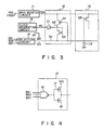
- Fig. 3 shows a sub-booster circuit according to a second embodiment of this invention and peripheral circuits thereof. Portions in Fig. 3 which correspond to those in Fig. 1 are denoted by the same reference numerals and the explanations thereof are therefore omitted.
- Depletion type N-channel MOS transistor Q4 having a gate grounded is connected between the output terminal of selection circuit 14 and node N1 of sub-booster circuit 12.
- sub-booster circuit 14 includes NAND gate (or NOR gate) 16 and CMOS inverter 17.
- Input terminals of NAND gate 16 are connected to receive selection signals SS1 to SSn (which can be replaced by address signals in the case of memory) which are used to select sub-booster circuit 12.
- an output potential of CMOS inverter 17 is set to a Vcc level (for example, 5 V), and when sub-booster circuit 12 is not selected, the output potential is set to 0 V.
- Vcc level for example, 5 V
- MOS capacitor C1 is formed to have the same structure as enhancement type MOS transistor Q2 so as to have threshold voltage V THC of 1 V, for example, MOS transistor Q1 is formed to have threshold voltage V TH1 of 0 V, and MOS transistor Q4 is formed in the same manner as a depletion type so as to have threshold voltage V TH4 of -3 V, for example.
- a sub-booster circuit which can step up an output voltage of a main booster circuit with a high step-up efficiency can be provided.
Landscapes
- Engineering & Computer Science (AREA)
- Power Engineering (AREA)
- Microelectronics & Electronic Packaging (AREA)
- Computer Hardware Design (AREA)
- Dc-Dc Converters (AREA)
- Read Only Memory (AREA)
- Metal-Oxide And Bipolar Metal-Oxide Semiconductor Integrated Circuits (AREA)
- Semiconductor Integrated Circuits (AREA)
- Semiconductor Memories (AREA)
- Non-Volatile Memory (AREA)
Applications Claiming Priority (2)
| Application Number | Priority Date | Filing Date | Title |
|---|---|---|---|
| JP101419/87 | 1987-04-24 | ||
| JP10141987A JPH0748310B2 (ja) | 1987-04-24 | 1987-04-24 | 半導体集積回路 |
Publications (3)
| Publication Number | Publication Date |
|---|---|
| EP0288075A2 true EP0288075A2 (de) | 1988-10-26 |
| EP0288075A3 EP0288075A3 (en) | 1990-10-17 |
| EP0288075B1 EP0288075B1 (de) | 1995-02-15 |
Family
ID=14300189
Family Applications (1)
| Application Number | Title | Priority Date | Filing Date |
|---|---|---|---|
| EP88106492A Expired - Lifetime EP0288075B1 (de) | 1987-04-24 | 1988-04-22 | Zusatz-Boosterschaltung zum Anheben der Ausgangsspannung einer Haupt-Boosterspannung |
Country Status (5)
| Country | Link |
|---|---|
| US (1) | US4905314A (de) |
| EP (1) | EP0288075B1 (de) |
| JP (1) | JPH0748310B2 (de) |
| KR (1) | KR910003387B1 (de) |
| DE (1) | DE3853016T2 (de) |
Cited By (2)
| Publication number | Priority date | Publication date | Assignee | Title |
|---|---|---|---|---|
| EP0640985A3 (de) * | 1993-08-23 | 1996-07-10 | Advanced Micro Devices Inc | Verteilte negative Torstromversorgung. |
| US5633134A (en) * | 1992-10-06 | 1997-05-27 | Ig Laboratories, Inc. | Method for simultaneously detecting multiple mutations in a DNA sample |
Families Citing this family (9)
| Publication number | Priority date | Publication date | Assignee | Title |
|---|---|---|---|---|
| JP3059737B2 (ja) * | 1989-12-25 | 2000-07-04 | シャープ株式会社 | 半導体記憶装置 |
| EP0954102A1 (de) * | 1991-12-09 | 1999-11-03 | Fujitsu Limited | Exklusiv-NOR-Gatter |
| US5255224A (en) * | 1991-12-18 | 1993-10-19 | International Business Machines Corporation | Boosted drive system for master/local word line memory architecture |
| KR940008206B1 (ko) * | 1991-12-28 | 1994-09-08 | 삼성전자 주식회사 | 고전압 스위치 회로 |
| KR960012789B1 (ko) * | 1993-12-01 | 1996-09-24 | 현대전자산업 주식회사 | 부트스트랩 회로 |
| KR100307514B1 (ko) * | 1994-07-30 | 2001-12-01 | 김영환 | 차지펌프회로 |
| JP3378457B2 (ja) * | 1997-02-26 | 2003-02-17 | 株式会社東芝 | 半導体装置 |
| JP2001160295A (ja) * | 1999-12-01 | 2001-06-12 | Toshiba Corp | 半導体集積回路 |
| US6788578B1 (en) | 2003-01-27 | 2004-09-07 | Turbo Ic, Inc. | Charge pump for conductive lines in programmable memory array |
Family Cites Families (9)
| Publication number | Priority date | Publication date | Assignee | Title |
|---|---|---|---|---|
| JPS5693422A (en) * | 1979-12-05 | 1981-07-29 | Fujitsu Ltd | Level-up circuit |
| JPS56129570A (en) * | 1980-03-14 | 1981-10-09 | Mitsubishi Electric Corp | Booster circuit |
| US4725746A (en) * | 1981-10-20 | 1988-02-16 | Kabushiki Kaisha Toshiba | MOSFET buffer circuit with an improved bootstrapping circuit |
| US4511811A (en) * | 1982-02-08 | 1985-04-16 | Seeq Technology, Inc. | Charge pump for providing programming voltage to the word lines in a semiconductor memory array |
| JPS58184821A (ja) * | 1982-03-31 | 1983-10-28 | Fujitsu Ltd | 昇圧回路 |
| JPS59124095A (ja) * | 1982-12-29 | 1984-07-18 | Fujitsu Ltd | 半導体記憶装置 |
| US4716303A (en) * | 1985-05-01 | 1987-12-29 | Sharp Kabushiki Kaisha | MOS IC pull-up circuit |
| JPS61260717A (ja) * | 1985-05-14 | 1986-11-18 | Mitsubishi Electric Corp | 半導体昇圧信号発生回路 |
| US4689495A (en) * | 1985-06-17 | 1987-08-25 | Advanced Micro Devices, Inc. | CMOS high voltage switch |
-
1987
- 1987-04-24 JP JP10141987A patent/JPH0748310B2/ja not_active Expired - Lifetime
-
1988
- 1988-04-21 US US07/184,580 patent/US4905314A/en not_active Expired - Lifetime
- 1988-04-22 EP EP88106492A patent/EP0288075B1/de not_active Expired - Lifetime
- 1988-04-22 DE DE3853016T patent/DE3853016T2/de not_active Expired - Lifetime
- 1988-04-23 KR KR1019880004663A patent/KR910003387B1/ko not_active Expired
Cited By (2)
| Publication number | Priority date | Publication date | Assignee | Title |
|---|---|---|---|---|
| US5633134A (en) * | 1992-10-06 | 1997-05-27 | Ig Laboratories, Inc. | Method for simultaneously detecting multiple mutations in a DNA sample |
| EP0640985A3 (de) * | 1993-08-23 | 1996-07-10 | Advanced Micro Devices Inc | Verteilte negative Torstromversorgung. |
Also Published As
| Publication number | Publication date |
|---|---|
| US4905314A (en) | 1990-02-27 |
| DE3853016D1 (de) | 1995-03-23 |
| JPS63268196A (ja) | 1988-11-04 |
| EP0288075B1 (de) | 1995-02-15 |
| EP0288075A3 (en) | 1990-10-17 |
| DE3853016T2 (de) | 1995-07-20 |
| JPH0748310B2 (ja) | 1995-05-24 |
| KR910003387B1 (ko) | 1991-05-28 |
| KR880013173A (ko) | 1988-11-30 |
Similar Documents
| Publication | Publication Date | Title |
|---|---|---|
| US6538930B2 (en) | Charge pump circuit for generating positive and negative voltage with reverse current prevention circuit and a nonvolatile memory using the same | |
| US7372739B2 (en) | High voltage generation and regulation circuit in a memory device | |
| US4733371A (en) | Semiconductor memory device with high voltage switch | |
| JP2652694B2 (ja) | 昇圧回路 | |
| JP3881020B2 (ja) | プログラム可能論理回路用のプログラム可能不揮発性両方向スイッチ | |
| US6137344A (en) | High speed charge pump circuit having field effect transistors possessing an improved charge transfer efficiency | |
| JP2003217291A (ja) | 不揮発性半導体記憶装置の昇圧回路 | |
| EP0288075A2 (de) | Zusatz-Boosterschaltung zum Anheben der Ausgangsspannung einer Haupt-Boosterspannung | |
| US4667312A (en) | Charge pump method and apparatus | |
| EP0280883A2 (de) | Halbleiter-Festwertspeichereinrichtung | |
| EP0376065A2 (de) | Integrierte Halbleiterspeicherschaltung | |
| US4580067A (en) | MOS dynamic load circuit for switching high voltages and adapted for use with high threshold transistors | |
| JPH07234265A (ja) | テスト電位転送回路およびこれを用いた半導体記憶装置 | |
| EP1041705A2 (de) | Ladungspumpenschaltung | |
| JPH0766675B2 (ja) | プログラマブルrom | |
| JP4243027B2 (ja) | 改良されたワードラインブースト回路 | |
| JPS6027118B2 (ja) | 半導体メモリ装置 | |
| KR0157343B1 (ko) | 반도체 메모리장치의 고전압 스위치 회로 | |
| JPH06111591A (ja) | 半導体集積回路 | |
| JPH1069796A (ja) | 高速試験機能付半導体集積回路 | |
| US6154084A (en) | Method for switching voltages higher than a supply voltage on a semiconductor chip with a circuit configuration | |
| JPH07321293A (ja) | 電源選択回路 | |
| EP0477896B1 (de) | Nichtflüchtige Halbleiterspeicheranordnung | |
| US6157225A (en) | Driving circuit with three output levels, one output level being a boosted level | |
| JPH01194861A (ja) | 昇圧回路 |
Legal Events
| Date | Code | Title | Description |
|---|---|---|---|
| PUAI | Public reference made under article 153(3) epc to a published international application that has entered the european phase |
Free format text: ORIGINAL CODE: 0009012 |
|
| 17P | Request for examination filed |
Effective date: 19880422 |
|
| AK | Designated contracting states |
Kind code of ref document: A2 Designated state(s): DE FR GB |
|
| PUAL | Search report despatched |
Free format text: ORIGINAL CODE: 0009013 |
|
| AK | Designated contracting states |
Kind code of ref document: A3 Designated state(s): DE FR GB |
|
| 17Q | First examination report despatched |
Effective date: 19920706 |
|
| RAP1 | Party data changed (applicant data changed or rights of an application transferred) |
Owner name: KABUSHIKI KAISHA TOSHIBA Owner name: TOSHIBA MICRO-ELECTRONICS CORPORATION |
|
| GRAA | (expected) grant |
Free format text: ORIGINAL CODE: 0009210 |
|
| AK | Designated contracting states |
Kind code of ref document: B1 Designated state(s): DE FR GB |
|
| REF | Corresponds to: |
Ref document number: 3853016 Country of ref document: DE Date of ref document: 19950323 |
|
| ET | Fr: translation filed | ||
| PLBE | No opposition filed within time limit |
Free format text: ORIGINAL CODE: 0009261 |
|
| STAA | Information on the status of an ep patent application or granted ep patent |
Free format text: STATUS: NO OPPOSITION FILED WITHIN TIME LIMIT |
|
| 26N | No opposition filed | ||
| REG | Reference to a national code |
Ref country code: GB Ref legal event code: IF02 |
|
| PGFP | Annual fee paid to national office [announced via postgrant information from national office to epo] |
Ref country code: DE Payment date: 20070419 Year of fee payment: 20 |
|
| PGFP | Annual fee paid to national office [announced via postgrant information from national office to epo] |
Ref country code: GB Payment date: 20070418 Year of fee payment: 20 |
|
| PGFP | Annual fee paid to national office [announced via postgrant information from national office to epo] |
Ref country code: FR Payment date: 20070411 Year of fee payment: 20 |
|
| REG | Reference to a national code |
Ref country code: GB Ref legal event code: PE20 Expiry date: 20080421 |
|
| PG25 | Lapsed in a contracting state [announced via postgrant information from national office to epo] |
Ref country code: GB Free format text: LAPSE BECAUSE OF EXPIRATION OF PROTECTION Effective date: 20080421 |