EP0296754A2 - Procédé de fabrication de dispositifs semi-conducteurs ayant des régions d'isolation comportant des rainures - Google Patents
Procédé de fabrication de dispositifs semi-conducteurs ayant des régions d'isolation comportant des rainures Download PDFInfo
- Publication number
- EP0296754A2 EP0296754A2 EP88305465A EP88305465A EP0296754A2 EP 0296754 A2 EP0296754 A2 EP 0296754A2 EP 88305465 A EP88305465 A EP 88305465A EP 88305465 A EP88305465 A EP 88305465A EP 0296754 A2 EP0296754 A2 EP 0296754A2
- Authority
- EP
- European Patent Office
- Prior art keywords
- layer
- corners
- trench region
- forming
- trench
- Prior art date
- Legal status (The legal status is an assumption and is not a legal conclusion. Google has not performed a legal analysis and makes no representation as to the accuracy of the status listed.)
- Granted
Links
Images



Classifications
-
- H—ELECTRICITY
- H10—SEMICONDUCTOR DEVICES; ELECTRIC SOLID-STATE DEVICES NOT OTHERWISE PROVIDED FOR
- H10P—GENERIC PROCESSES OR APPARATUS FOR THE MANUFACTURE OR TREATMENT OF DEVICES COVERED BY CLASS H10
- H10P90/00—Preparation of wafers not covered by a single main group of this subclass, e.g. wafer reinforcement
- H10P90/19—Preparing inhomogeneous wafers
- H10P90/1904—Preparing vertically inhomogeneous wafers
- H10P90/1906—Preparing SOI wafers
-
- H—ELECTRICITY
- H10—SEMICONDUCTOR DEVICES; ELECTRIC SOLID-STATE DEVICES NOT OTHERWISE PROVIDED FOR
- H10W—GENERIC PACKAGES, INTERCONNECTIONS, CONNECTORS OR OTHER CONSTRUCTIONAL DETAILS OF DEVICES COVERED BY CLASS H10
- H10W10/00—Isolation regions in semiconductor bodies between components of integrated devices
- H10W10/01—Manufacture or treatment
- H10W10/011—Manufacture or treatment of isolation regions comprising dielectric materials
- H10W10/012—Manufacture or treatment of isolation regions comprising dielectric materials using local oxidation of silicon [LOCOS]
- H10W10/0121—Manufacture or treatment of isolation regions comprising dielectric materials using local oxidation of silicon [LOCOS] in regions recessed from the surface, e.g. in trenches or grooves
-
- H—ELECTRICITY
- H10—SEMICONDUCTOR DEVICES; ELECTRIC SOLID-STATE DEVICES NOT OTHERWISE PROVIDED FOR
- H10W—GENERIC PACKAGES, INTERCONNECTIONS, CONNECTORS OR OTHER CONSTRUCTIONAL DETAILS OF DEVICES COVERED BY CLASS H10
- H10W10/00—Isolation regions in semiconductor bodies between components of integrated devices
- H10W10/01—Manufacture or treatment
- H10W10/011—Manufacture or treatment of isolation regions comprising dielectric materials
- H10W10/014—Manufacture or treatment of isolation regions comprising dielectric materials using trench refilling with dielectric materials, e.g. shallow trench isolations
-
- H—ELECTRICITY
- H10—SEMICONDUCTOR DEVICES; ELECTRIC SOLID-STATE DEVICES NOT OTHERWISE PROVIDED FOR
- H10W—GENERIC PACKAGES, INTERCONNECTIONS, CONNECTORS OR OTHER CONSTRUCTIONAL DETAILS OF DEVICES COVERED BY CLASS H10
- H10W10/00—Isolation regions in semiconductor bodies between components of integrated devices
- H10W10/01—Manufacture or treatment
- H10W10/041—Manufacture or treatment of isolation regions comprising polycrystalline semiconductor materials
-
- H—ELECTRICITY
- H10—SEMICONDUCTOR DEVICES; ELECTRIC SOLID-STATE DEVICES NOT OTHERWISE PROVIDED FOR
- H10W—GENERIC PACKAGES, INTERCONNECTIONS, CONNECTORS OR OTHER CONSTRUCTIONAL DETAILS OF DEVICES COVERED BY CLASS H10
- H10W10/00—Isolation regions in semiconductor bodies between components of integrated devices
- H10W10/01—Manufacture or treatment
- H10W10/061—Manufacture or treatment using SOI processes together with lateral isolation, e.g. combinations of SOI and shallow trench isolations
-
- H—ELECTRICITY
- H10—SEMICONDUCTOR DEVICES; ELECTRIC SOLID-STATE DEVICES NOT OTHERWISE PROVIDED FOR
- H10W—GENERIC PACKAGES, INTERCONNECTIONS, CONNECTORS OR OTHER CONSTRUCTIONAL DETAILS OF DEVICES COVERED BY CLASS H10
- H10W10/00—Isolation regions in semiconductor bodies between components of integrated devices
- H10W10/10—Isolation regions comprising dielectric materials
- H10W10/13—Isolation regions comprising dielectric materials formed using local oxidation of silicon [LOCOS], e.g. sealed interface localised oxidation [SILO] or side-wall mask isolation [SWAMI]
-
- H—ELECTRICITY
- H10—SEMICONDUCTOR DEVICES; ELECTRIC SOLID-STATE DEVICES NOT OTHERWISE PROVIDED FOR
- H10W—GENERIC PACKAGES, INTERCONNECTIONS, CONNECTORS OR OTHER CONSTRUCTIONAL DETAILS OF DEVICES COVERED BY CLASS H10
- H10W10/00—Isolation regions in semiconductor bodies between components of integrated devices
- H10W10/10—Isolation regions comprising dielectric materials
- H10W10/17—Isolation regions comprising dielectric materials formed using trench refilling with dielectric materials, e.g. shallow trench isolations
-
- H—ELECTRICITY
- H10—SEMICONDUCTOR DEVICES; ELECTRIC SOLID-STATE DEVICES NOT OTHERWISE PROVIDED FOR
- H10W—GENERIC PACKAGES, INTERCONNECTIONS, CONNECTORS OR OTHER CONSTRUCTIONAL DETAILS OF DEVICES COVERED BY CLASS H10
- H10W10/00—Isolation regions in semiconductor bodies between components of integrated devices
- H10W10/10—Isolation regions comprising dielectric materials
- H10W10/181—Semiconductor-on-insulator [SOI] isolation regions, e.g. buried oxide regions of SOI wafers
-
- H—ELECTRICITY
- H10—SEMICONDUCTOR DEVICES; ELECTRIC SOLID-STATE DEVICES NOT OTHERWISE PROVIDED FOR
- H10W—GENERIC PACKAGES, INTERCONNECTIONS, CONNECTORS OR OTHER CONSTRUCTIONAL DETAILS OF DEVICES COVERED BY CLASS H10
- H10W10/00—Isolation regions in semiconductor bodies between components of integrated devices
- H10W10/40—Isolation regions comprising polycrystalline semiconductor materials
-
- H—ELECTRICITY
- H10—SEMICONDUCTOR DEVICES; ELECTRIC SOLID-STATE DEVICES NOT OTHERWISE PROVIDED FOR
- H10P—GENERIC PROCESSES OR APPARATUS FOR THE MANUFACTURE OR TREATMENT OF DEVICES COVERED BY CLASS H10
- H10P90/00—Preparation of wafers not covered by a single main group of this subclass, e.g. wafer reinforcement
- H10P90/19—Preparing inhomogeneous wafers
- H10P90/1904—Preparing vertically inhomogeneous wafers
- H10P90/1906—Preparing SOI wafers
- H10P90/1914—Preparing SOI wafers using bonding
-
- H—ELECTRICITY
- H10—SEMICONDUCTOR DEVICES; ELECTRIC SOLID-STATE DEVICES NOT OTHERWISE PROVIDED FOR
- H10W—GENERIC PACKAGES, INTERCONNECTIONS, CONNECTORS OR OTHER CONSTRUCTIONAL DETAILS OF DEVICES COVERED BY CLASS H10
- H10W10/00—Isolation regions in semiconductor bodies between components of integrated devices
- H10W10/01—Manufacture or treatment
- H10W10/011—Manufacture or treatment of isolation regions comprising dielectric materials
- H10W10/012—Manufacture or treatment of isolation regions comprising dielectric materials using local oxidation of silicon [LOCOS]
Definitions
- This invention concerns a method of manufacturing a semiconductor device and a device so manufactured. More particularly, this invention relates to a method of forming an improved trench region for the purpose of isolation of semiconductor elements formed in a semiconductor substrate.
- a trench method using trenches filled with a dielectric material and a polycrystalline silicon layer is used for the separation of semiconductor elements.
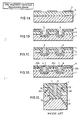
- Fig. 1 shows an example of a conventional trench method.
- an insulating layer 3 of sufficient thickness to serve as a mask layer for a following etching process is formed on the surface of the epitaxial growth layer 2 of P type (or N type) formed on the semiconductor substrate 1 of N type (or P type).
- the insulating layer 3 e.g., a silicon oxide layer, is selectively removed by conventional photo-etching techniques to expose the surface of the layer 2 where a trench region is to be formed, as shown in Fig 1A.
- an etching process is carried out to form trench regions 5 using the insulating layer 3 as the mask.
- the depth of the trench regions 5 is chosen approximately equal to the depth of an isolation region to be formed.
- an ion-implantation process using dopant of the same conductivity type to the substrate 1, is carried out to form a channel stopper region (not illustrated) beneath the trench region to reduce a parasitic MOS effect.
- an oxidation treatment is carried out to form an insulating layer 4 , e.g., a silicon oxide layer, for the purpose of protection and partial filling of the trench regions 5.
- a polycrystalline layer is formed to fill and cover the trench regions 5 , completely.
- an etching process is carried out to remove any excess polycrystalline layer above the top of the trench regions 5(FIG 1C) .
- an oxidation treatment is carried out to form an insulating layer 7 on the top surface of the polycrystalline layer 6 to get a flat surface as shown in FIG 1D .
- insulated island regions 201 , 202 and 203 are achieved.
- great stress is applied to the corner of the trench region 5 .
- stress concentration occurs at the corners. This stress causes crystal defects 19 in the island regions 201 , 202 and the substrate 1 , as shown in FIG 1E .
- another process using a thin insulating film has been used.
- FIG 2 shows an example using a thin insulating film 12 , e.g., less than 2000 ⁇ .
- FIG 2A shows a state after the formation of insulated island regions 11 and 14 .
- a thick insulating layer 16 such as a field oxide layer
- wedge-shaped insulating regions are formed at the corners of the island regions 11 and 14 , as illustrated by numeral 17(FIG 2B) .
- FIG 3 shows an improved conventional process to reduce the stress concentration at the corners of the trench region by rounding the corners thereof.
- an insulating layer 21 is formed, as illustrated in FIG 3B .
- the insulating layer 21 is removed, as illustrated in FIG 3C .
- the insulating layer 21 is formed by the reaction of oxygen diffused into the substrate 20 with the material, e.g., silicon, of the substrate 20 .
- the boundary between the insulating layer 21 and the substrate 20 are determined by the profile of the diffused oxygen.
- the constant density line of the diffused oxygen at the corners is round, the formation of a rounded corner would be expected.
- stress is also applied to the substrate. The more the stress is applied, slower the growth rate of the insulating layer becomes.
- the growth rate of the insulating layer at the edge of the corners is slower than that at other portions.
- a sharp portion is formed at the corner of the trench region, as illustrated in FIG 3D . This process is also insufficient to round the corner.
- the sharp portion causes a concentration of the electric field.
- an object of this invention is to provide a method for effectively rounding the corners of the trench region.
- the corners of the trench region are effectively rounded by, preparing a semiconductor substrate having a first surface; forming a trench region in the first surface of the substrate, having corners at the intersections of the trench region with the first surface; forming a first polycrystalline layer over the first surface covering the corners of, and only partially filling the trench region, and oxidizing the first polycrystalline layer, thereby rounding the corners of the trench region and only partially filling the trench region.
- a thick insulating film can be formed without causing stress concentrations towards the corners of the trench region. Furthermore, the rounded corners reduce the electric concentration when a trench capacitor is formed at the trench region. Thus, the break down voltage of the trench capacitor is increased.
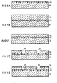
- FIGS 4A to 4F One embodiment of this invention is illustrated in FIGS 4A to 4F .
- a semiconductor substrate 24 of a first conductivity type e.g., P type or N type is prepared.
- an epitaxial layer 23 of a second conductivity type, e.g., N type or P type, is formed on the semiconductor substrate 24 .
- the thickness of the epitaxial layer is chosen, e.g., between 1 to 2 ⁇ m.
- an insulating oxide layer 22 is formed by conventional oxidation treatment.
- the insulating layer 22 is partially removed to selectively expose the surface of the epitaxial layer 22 , as illustrated in FIG 4A , using a photo-etching process.
- an etching process is carried out to form trench regions 25 , as shown in FIG 4B .
- the depth of the trench region is chosen approximately equal to the depth of an isolation region to be formed.
- a dry etching process such as reactive ion etching (RIE) using the remaining insulating layer 22 as a mask, rather than a wet etching process using, e.g., HF and HNO3, so as to prevent side etching.
- RIE reactive ion etching
- the remaining insulating layer 22 is removed.
- a polycrystalline layer 27 is deposited over the surface by chemical vapor deposition (CVD). In this case, because of the property of the polycrystalline layer of covering the corner roundly, the corner of the trench region after the formation of the polycrystalline layer 27 becomes round.
- a low pressure CVD e.g., under a reduced pressure of about 150m Torr
- the thickness of the polycrystalline layer 27 should be chosen considering the width of the trench region 25 . For example, when the width of the trench region 25 is between 1 and 1.5 ⁇ m, the thickness of the polycrystalline layer 27 is selected between a few hundred ⁇ and 3,000 ⁇ .
- an oxidation treatment is carried out to convert the polycrystalline layer 27 into an insulating oxide layer 28 to fill partially the trench regions 25 , as shown in FIG 4D . In the case where the insulating oxide layer 28 fills the trench regions 25 completely, great stress occurs within the trench regions 25 .
- the epitaxial layer 23 from the side thereof.
- a part of the substrate 24 and the epitaxial layer 23 is also oxidized.
- the stress concentrations at the corners during the formation of the insulating oxide layer 28 are reduced.
- the oxidation of the corners of epitaxial layer 23 is done substantially according to the oxygen profile diffused into the epitaxial layer 23 .
- the oxygen profile at the corners of the epitaxial layer 23 is round, the corners of the epitaxial layer after the oxidation become round.
- the insulating oxide layer 28 is removed by an etching process, e.g., wet etching using HF etchant, as shown in FIG 4E .
- an etching process e.g., wet etching using HF etchant
- the shape of the corners after the removal of the insulating oxide layer 28 is round.
- oxidation treatment is carried out to form an insulating oxide layer 29 serving as a protection layer of the trench region 25 and as a field oxide layer. In this oxidation treatment, as the corners of the epitaxial layer 23 are round, the stress towards the corners at the oxidation treatment is reduced.
- the thickness of the insulation layer 29 is chosen between 8,000 and 10,000 ⁇ , for example.
- a polycrystalline layer of sufficient thickness to fill the trench region is deposited by a CVD process. It is preferable to choose a thickness of the polycrystalline layer of more than 1.2 to 1.5 times the width of the trench region after the formation of the insulating oxide layer 29 to obtain a flat surface.
- an etching process e.g., a plasma etching process, is performed to remove the excess polycrystalline layer over the insulating layer 29 .
- an oxidation treatment is carried out to form an insulating oxide layer 31 at the surface of the polycrystalline layer 30 , as shown in FIG 4H .
- epitaxial island regions 301 , 302 and 303 are achieved.
- circuit elements are formed in these island regions (not illustrated).
- FIGS 5A to 5I shows another embodiment of this invention.
- a semiconductor wafer 51 of about 450 to 625 ⁇ m of a first conductivity type, e.g.,P type or N type is prepared.
- an oxidation treatment at a temperature of about 1100°C is carried out to form an insulating oxide film 52 of about 1 ⁇ m thickness over the surface of the semiconductor wafter 51 , as shown in FIG 5A .
- a second semiconductor wafer 53 having a mirror face, of P type or N type is positioned on the insulating layer 52 so as to face the mirror face to the insulating layer 52 .
- an annealing process of about 2 hours at a temperature of 1100°C in nitrogen atmosphere is carried out to provide a combination structure of two wafers 51 , 53 and an insulating oxide layer 52 , as shown in FIG 5B .
- an etching process including a lapping process, is applied to the wafer 53 to produce a semiconductor layer 54 of about 20 ⁇ m thickness.
- an anisotropic etching process such as RIE, is carried out to form trench regions 55 of about 1 ⁇ m width as shown in FIG 5D .
- an oxidation treatment at a temperature of about 1,000°C is carried out to form a thin oxide layer 56 of about 200 ⁇ thickness at the surface of the semiconductor substrate 54 , as shown in FIG 5E .
- a polycrystalline layer 57 of about 2,000 ⁇ thickness is formed over the entire surface, as shown in FIG 5F .
- LPCVD of about 150 m Torr, to improve the coverage of the polycrystalline layer at the corners of the trench region.
- the structure is then subjected to an oxidation treatment at a temperature of about 1,100°C to convert the polycrystalline layer 57 into an insulating oxide layer.
- the numeral 58 designates the total insulating oxide layer of the insulating layer 56 , the converted insulating oxide layer of the polycrystalline layer 57 and the oxide layer of the semiconductor layer 54 formed during the oxidation process of the polycrystalline layer 57 .
- the oxidation at the corners of semiconductor layer 54 is done substantially according to the oxygen profile diffused into the semiconductor region 54 .
- the oxygen profile at the corners of the semiconductor region 54 is round, the corners of the semiconductor region after the oxidation of the semiconductor region 54 become round.
- a polycrystalline layer is formed over the surface. It is preferable to choose a thickness of the polycrystalline layer of more than 1.2 to 1.5 times the width of the trench region after the formation of the insulating oxide layer 58 . Then, an etching process is carried out to remove the excess polycrystalline layer over the insulating layer 58 to produce a flat surface. Next, the construction is subjected to an oxidation treatment to form an insulating oxide layer at the surface of the polycrystalline layer 59. In this way, island regions 501, 502 and 503 surrounded by insulating material, are achieved, as shown in Fig 5H. In this embodiment, the property of the polycrystalline layer of covering the corners of trench region roundly is used, also.
- the insulating layer 52 is etched during the etching process for forming the trench regions 55.
- an overhanging structure of the island regions 501, 502 at the bottom of the trench region 55 is formed, as shown in Fig. 5I.
- the bottom corners of the semiconductor layer 54 also are covered roundly with the polycrystalline layer 57.
- the stress concentration during formation of the thick insulating layer 58 at the bottom corners of the semiconductor region 54 is also reduced.
Landscapes
- Element Separation (AREA)
- Semiconductor Integrated Circuits (AREA)
Applications Claiming Priority (2)
| Application Number | Priority Date | Filing Date | Title |
|---|---|---|---|
| JP62150281A JPS63314844A (ja) | 1987-06-18 | 1987-06-18 | 半導体装置の製造方法 |
| JP150281/87 | 1987-06-18 |
Publications (3)
| Publication Number | Publication Date |
|---|---|
| EP0296754A2 true EP0296754A2 (fr) | 1988-12-28 |
| EP0296754A3 EP0296754A3 (en) | 1990-08-01 |
| EP0296754B1 EP0296754B1 (fr) | 1996-08-14 |
Family
ID=15493543
Family Applications (1)
| Application Number | Title | Priority Date | Filing Date |
|---|---|---|---|
| EP88305465A Expired - Lifetime EP0296754B1 (fr) | 1987-06-18 | 1988-06-15 | Procédé de fabrication de dispositifs semi-conducteurs ayant des régions d'isolation comportant des rainures |
Country Status (5)
| Country | Link |
|---|---|
| US (1) | US4916086A (fr) |
| EP (1) | EP0296754B1 (fr) |
| JP (1) | JPS63314844A (fr) |
| KR (1) | KR920001033B1 (fr) |
| DE (1) | DE3855469T2 (fr) |
Cited By (19)
| Publication number | Priority date | Publication date | Assignee | Title |
|---|---|---|---|---|
| DE3902701A1 (de) * | 1988-01-30 | 1989-08-10 | Toshiba Kawasaki Kk | Verfahren zur herstellung einer halbleiteranordnung |
| EP0444836A3 (en) * | 1990-02-23 | 1991-11-06 | Sharp Kabushiki Kaisha | Process for forming semiconductor device isolation regions |
| EP0437950A3 (en) * | 1989-12-20 | 1992-04-22 | Fujitsu Limited | Semiconductor device having silicon-on-insulator structure and method of producing the same |
| EP0485719A2 (fr) * | 1990-11-16 | 1992-05-20 | Shin-Etsu Handotai Company Limited | Substrat avec isolation diélectrique et procédé de sa fabrication |
| EP0392468A3 (fr) * | 1989-04-10 | 1992-07-08 | Kabushiki Kaisha Toshiba | Dispositif semi-conducteur à plusieurs composants comportant une couche d'isolation électrique |
| EP0423722A3 (en) * | 1989-10-16 | 1993-01-13 | Kabushiki Kaisha Toshiba | Method of making complete dielectric isolation structure in semiconductor integrated circuit |
| EP0464837A3 (en) * | 1990-07-05 | 1993-01-27 | Kabushiki Kaisha Toshiba | Method of manufacturing semiconductor substrate using semiconductor integrated circuit having dielectric separation structure |
| EP0469583A3 (en) * | 1990-07-31 | 1993-02-03 | Kabushiki Kaisha Toshiba | Semiconductor substrate with complete dielectric isolation structure and method of making the same |
| EP0421703A3 (en) * | 1989-10-02 | 1993-03-10 | Motorola, Inc. | Encapsulation method for localized oxidation of silicon |
| EP0386778B1 (fr) * | 1989-03-09 | 1993-07-28 | Tanabe Seiyaku Co., Ltd. | Dérivés biphényliques |
| US5250836A (en) * | 1989-12-20 | 1993-10-05 | Fujitsu Limited | Semiconductor device having silicon-on-insulator structure |
| EP0451454A3 (en) * | 1990-02-09 | 1994-08-24 | Toshiba Kk | Semiconductor device having element regions being electrically isolated from each other |
| EP0445471A3 (en) * | 1990-03-06 | 1994-10-26 | Digital Equipment Corp | Method of forming isolation trenches in a semiconductor substrate |
| EP0631305A1 (fr) * | 1993-06-23 | 1994-12-28 | Siemens Aktiengesellschaft | Procédé de fabrication d'une région d'isolation dans un substrat pour la technologie de puissance intélligente |
| EP0631306A1 (fr) * | 1993-06-23 | 1994-12-28 | Siemens Aktiengesellschaft | Procédé de fabrication d'une région d'isolation dans un substrat pour la technologie de puissance intélligente |
| EP0645808A1 (fr) * | 1993-09-27 | 1995-03-29 | Siemens Aktiengesellschaft | Procédé de fabrication d'une rainure d'isolation dans un substrat du type SOI |
| EP0735580A1 (fr) * | 1995-03-31 | 1996-10-02 | Co.Ri.M.Me. Consorzio Per La Ricerca Sulla Microelettronica Nel Mezzogiorno | Procédé de formation de rainures d'isolation |
| EP0736897A3 (fr) * | 1995-04-04 | 1998-03-11 | Motorola, Inc. | Procédé pour former une structure de rainure pour isolation pour circuit intégré |
| US6524931B1 (en) | 1999-07-20 | 2003-02-25 | Motorola, Inc. | Method for forming a trench isolation structure in an integrated circuit |
Families Citing this family (24)
| Publication number | Priority date | Publication date | Assignee | Title |
|---|---|---|---|---|
| US5332683A (en) * | 1989-06-14 | 1994-07-26 | Kabushiki Kaisha Toshiba | Method of manufacturing semiconductor device having elements isolated by trench |
| FR2651068B1 (fr) * | 1989-08-16 | 1994-06-10 | France Etat | Procede de fabrication de transistor mos mesa de type silicium sur isolant |
| KR960006714B1 (ko) * | 1990-05-28 | 1996-05-22 | 가부시끼가이샤 도시바 | 반도체 장치의 제조 방법 |
| JPH05304202A (ja) * | 1992-04-02 | 1993-11-16 | Nec Corp | 半導体装置の製造方法 |
| EP0603106A2 (fr) * | 1992-12-16 | 1994-06-22 | International Business Machines Corporation | Procédé pour réduire le stress d'une structure de rainure pour un substrat du type SOI |
| JP2955459B2 (ja) * | 1993-12-20 | 1999-10-04 | 株式会社東芝 | 半導体装置の製造方法 |
| JP3396553B2 (ja) * | 1994-02-04 | 2003-04-14 | 三菱電機株式会社 | 半導体装置の製造方法及び半導体装置 |
| US5472902A (en) * | 1994-03-21 | 1995-12-05 | United Microelectronics Corp. | Silicon-on-insulator isolation technology using liquid phase deposition |
| JPH07326664A (ja) * | 1994-05-31 | 1995-12-12 | Fuji Electric Co Ltd | ウエハの誘電体分離溝の充填方法 |
| TW350122B (en) * | 1997-02-14 | 1999-01-11 | Winbond Electronics Corp | Method of forming a shallow groove |
| US5811346A (en) * | 1997-04-14 | 1998-09-22 | Vlsi Technology, Inc. | Silicon corner rounding in shallow trench isolation process |
| US5994229A (en) * | 1998-01-12 | 1999-11-30 | Taiwan Semiconductor Manufacturing Company Ltd. | Achievement of top rounding in shallow trench etch |
| JP3917327B2 (ja) * | 1999-06-01 | 2007-05-23 | 株式会社ルネサステクノロジ | 半導体装置の製造方法及び装置 |
| US20020102500A1 (en) * | 2001-01-31 | 2002-08-01 | Lian-Fa Hung | Method for raising etching selectivity of oxide to photoresist |
| US6524929B1 (en) | 2001-02-26 | 2003-02-25 | Advanced Micro Devices, Inc. | Method for shallow trench isolation using passivation material for trench bottom liner |
| US6486038B1 (en) * | 2001-03-12 | 2002-11-26 | Advanced Micro Devices | Method for and device having STI using partial etch trench bottom liner |
| US6521510B1 (en) * | 2001-03-23 | 2003-02-18 | Advanced Micro Devices, Inc. | Method for shallow trench isolation with removal of strained island edges |
| US6534379B1 (en) | 2001-03-26 | 2003-03-18 | Advanced Micro Devices, Inc. | Linerless shallow trench isolation method |
| US6583488B1 (en) | 2001-03-26 | 2003-06-24 | Advanced Micro Devices, Inc. | Low density, tensile stress reducing material for STI trench fill |
| KR100416795B1 (ko) * | 2001-04-27 | 2004-01-31 | 삼성전자주식회사 | 소자분리막 형성방법 및 이를 이용한 반도체 장치의제조방법 |
| US6562696B1 (en) * | 2002-03-06 | 2003-05-13 | Taiwan Semiconductor Manufacturing Co., Ltd | Method for forming an STI feature to avoid acidic etching of trench sidewalls |
| US6902867B2 (en) * | 2002-10-02 | 2005-06-07 | Lexmark International, Inc. | Ink jet printheads and methods therefor |
| US7129149B1 (en) | 2004-06-07 | 2006-10-31 | Integrated Device Technology, Inc. | Method for forming shallow trench isolation structure with anti-reflective liner |
| US7176104B1 (en) | 2004-06-08 | 2007-02-13 | Integrated Device Technology, Inc. | Method for forming shallow trench isolation structure with deep oxide region |
Family Cites Families (9)
| Publication number | Priority date | Publication date | Assignee | Title |
|---|---|---|---|---|
| JPS53148988A (en) * | 1977-05-31 | 1978-12-26 | Matsushita Electric Ind Co Ltd | Manufacture of semiconductor substrate |
| JPS5864045A (ja) * | 1981-10-14 | 1983-04-16 | Fujitsu Ltd | 半導体装置の製造方法 |
| JPS58168233A (ja) * | 1982-03-30 | 1983-10-04 | Fujitsu Ltd | 半導体装置の製造方法 |
| JPS60223153A (ja) * | 1984-04-19 | 1985-11-07 | Nippon Telegr & Teleph Corp <Ntt> | Mis型キャパシタを有する半導体装置の製法 |
| JPS61176133A (ja) * | 1985-01-31 | 1986-08-07 | Toshiba Corp | 半導体装置の製造方法 |
| US4621414A (en) * | 1985-03-04 | 1986-11-11 | Advanced Micro Devices, Inc. | Method of making an isolation slot for integrated circuit structure |
| US4666556A (en) * | 1986-05-12 | 1987-05-19 | International Business Machines Corporation | Trench sidewall isolation by polysilicon oxidation |
| US4693781A (en) * | 1986-06-26 | 1987-09-15 | Motorola, Inc. | Trench formation process |
| GB2200794A (en) * | 1986-11-19 | 1988-08-10 | Plessey Co Plc | Semiconductor device manufacture |
-
1987
- 1987-06-18 JP JP62150281A patent/JPS63314844A/ja active Granted
-
1988
- 1988-06-09 US US07/204,550 patent/US4916086A/en not_active Expired - Lifetime
- 1988-06-15 DE DE3855469T patent/DE3855469T2/de not_active Expired - Lifetime
- 1988-06-15 EP EP88305465A patent/EP0296754B1/fr not_active Expired - Lifetime
- 1988-06-18 KR KR1019880007354A patent/KR920001033B1/ko not_active Expired
Cited By (25)
| Publication number | Priority date | Publication date | Assignee | Title |
|---|---|---|---|---|
| DE3902701A1 (de) * | 1988-01-30 | 1989-08-10 | Toshiba Kawasaki Kk | Verfahren zur herstellung einer halbleiteranordnung |
| EP0386778B1 (fr) * | 1989-03-09 | 1993-07-28 | Tanabe Seiyaku Co., Ltd. | Dérivés biphényliques |
| EP0392468A3 (fr) * | 1989-04-10 | 1992-07-08 | Kabushiki Kaisha Toshiba | Dispositif semi-conducteur à plusieurs composants comportant une couche d'isolation électrique |
| EP0421703A3 (en) * | 1989-10-02 | 1993-03-10 | Motorola, Inc. | Encapsulation method for localized oxidation of silicon |
| EP0423722A3 (en) * | 1989-10-16 | 1993-01-13 | Kabushiki Kaisha Toshiba | Method of making complete dielectric isolation structure in semiconductor integrated circuit |
| EP0437950A3 (en) * | 1989-12-20 | 1992-04-22 | Fujitsu Limited | Semiconductor device having silicon-on-insulator structure and method of producing the same |
| US5250836A (en) * | 1989-12-20 | 1993-10-05 | Fujitsu Limited | Semiconductor device having silicon-on-insulator structure |
| EP0451454A3 (en) * | 1990-02-09 | 1994-08-24 | Toshiba Kk | Semiconductor device having element regions being electrically isolated from each other |
| US5116779A (en) * | 1990-02-23 | 1992-05-26 | Sharp Kabushiki Kaisha | Process for forming semiconductor device isolation regions |
| EP0444836A3 (en) * | 1990-02-23 | 1991-11-06 | Sharp Kabushiki Kaisha | Process for forming semiconductor device isolation regions |
| EP0445471A3 (en) * | 1990-03-06 | 1994-10-26 | Digital Equipment Corp | Method of forming isolation trenches in a semiconductor substrate |
| EP0464837A3 (en) * | 1990-07-05 | 1993-01-27 | Kabushiki Kaisha Toshiba | Method of manufacturing semiconductor substrate using semiconductor integrated circuit having dielectric separation structure |
| EP0469583A3 (en) * | 1990-07-31 | 1993-02-03 | Kabushiki Kaisha Toshiba | Semiconductor substrate with complete dielectric isolation structure and method of making the same |
| EP0485719A2 (fr) * | 1990-11-16 | 1992-05-20 | Shin-Etsu Handotai Company Limited | Substrat avec isolation diélectrique et procédé de sa fabrication |
| US5700712A (en) * | 1993-06-23 | 1997-12-23 | Siemens Aktiengesellschaft | Method for manufacturing an insulating trench in an SOI substrate for smartpower technologies |
| EP0631306A1 (fr) * | 1993-06-23 | 1994-12-28 | Siemens Aktiengesellschaft | Procédé de fabrication d'une région d'isolation dans un substrat pour la technologie de puissance intélligente |
| US5496765A (en) * | 1993-06-23 | 1996-03-05 | Siemens Aktiengesellschaft | Method for manufacturing an insulating trench in a substrate for smart-power technologies |
| EP0631305A1 (fr) * | 1993-06-23 | 1994-12-28 | Siemens Aktiengesellschaft | Procédé de fabrication d'une région d'isolation dans un substrat pour la technologie de puissance intélligente |
| EP0645808A1 (fr) * | 1993-09-27 | 1995-03-29 | Siemens Aktiengesellschaft | Procédé de fabrication d'une rainure d'isolation dans un substrat du type SOI |
| US5416041A (en) * | 1993-09-27 | 1995-05-16 | Siemens Aktiengesellschaft | Method for producing an insulating trench in an SOI substrate |
| EP0735580A1 (fr) * | 1995-03-31 | 1996-10-02 | Co.Ri.M.Me. Consorzio Per La Ricerca Sulla Microelettronica Nel Mezzogiorno | Procédé de formation de rainures d'isolation |
| US6001705A (en) * | 1995-03-31 | 1999-12-14 | Consorzio Per La Ricerca Sulla Microelettronica Nel Mezzogiorno | Process for realizing trench structures |
| US6362072B1 (en) | 1995-03-31 | 2002-03-26 | Stmicroelectronics S.R.L. | Process for realizing trench structures |
| EP0736897A3 (fr) * | 1995-04-04 | 1998-03-11 | Motorola, Inc. | Procédé pour former une structure de rainure pour isolation pour circuit intégré |
| US6524931B1 (en) | 1999-07-20 | 2003-02-25 | Motorola, Inc. | Method for forming a trench isolation structure in an integrated circuit |
Also Published As
| Publication number | Publication date |
|---|---|
| DE3855469D1 (de) | 1996-09-19 |
| DE3855469T2 (de) | 1997-02-13 |
| EP0296754B1 (fr) | 1996-08-14 |
| KR890001165A (ko) | 1989-03-18 |
| JPH0423422B2 (fr) | 1992-04-22 |
| EP0296754A3 (en) | 1990-08-01 |
| KR920001033B1 (ko) | 1992-02-01 |
| US4916086A (en) | 1990-04-10 |
| JPS63314844A (ja) | 1988-12-22 |
Similar Documents
| Publication | Publication Date | Title |
|---|---|---|
| US4916086A (en) | Method of manufacturing a semiconductor device having rounded trench corners | |
| US6174785B1 (en) | Method of forming trench isolation region for semiconductor device | |
| US5084408A (en) | Method of making complete dielectric isolation structure in semiconductor integrated circuit | |
| EP0048175B1 (fr) | Dispositif semi-conducteur et procédé pour sa fabrication | |
| KR100338767B1 (ko) | 트렌치 소자분리 구조와 이를 갖는 반도체 소자 및 트렌치 소자분리 방법 | |
| JP2554831B2 (ja) | 基板分離トレンチを形成するための半導体処理方法 | |
| US4771328A (en) | Semiconductor device and process | |
| JPH104136A (ja) | 半導体装置の素子分離膜の形成方法 | |
| CN87104640A (zh) | 集成电路绝缘工艺方法 | |
| KR100278729B1 (ko) | 집적 회로에서의 전기적 분리 구조체 형성 방법 | |
| US4916087A (en) | Method of manufacturing a semiconductor device by filling and planarizing narrow and wide trenches | |
| JPH11111710A (ja) | 半導体装置およびその製造方法 | |
| US4876214A (en) | Method for fabricating an isolation region in a semiconductor substrate | |
| US6130467A (en) | Shallow trench isolation with spacers for improved gate oxide quality | |
| EP0645809B1 (fr) | Procédé pour fabriquer un dispositif semi-conducteur comportant un corps semi-conducteur comportant des régions d'isolation de champ formées par des rainures remplies de matériau isolant | |
| US5641704A (en) | Method of isolating active areas of a semiconductor substrate by shallow trenches and narrow trenches | |
| EP0095328B1 (fr) | Procédé de réalisation d'un dispositif semi-conducteur par le contrôle de l'épaisseur de la couche isolante sur la partie périphérique de l'élement | |
| EP0641022B1 (fr) | Structure d'isolation et procédé de sa fabrication | |
| US6486038B1 (en) | Method for and device having STI using partial etch trench bottom liner | |
| US5472902A (en) | Silicon-on-insulator isolation technology using liquid phase deposition | |
| EP1067599B1 (fr) | Méthode de formation de structures comportant des régions oxidées enfouies dans un substrat semiconducteur | |
| EP0402897B1 (fr) | Procédé pour la fabrication de dispositifs semi-conducteurs comportant des composants isolés par des rainures | |
| EP0137195B1 (fr) | Cicuit à isolement diélectrique et procédé de fabrication | |
| US6261966B1 (en) | Method for improving trench isolation | |
| KR100191713B1 (ko) | 반도체 소자의 필드 산화막 형성방법 |
Legal Events
| Date | Code | Title | Description |
|---|---|---|---|
| PUAI | Public reference made under article 153(3) epc to a published international application that has entered the european phase |
Free format text: ORIGINAL CODE: 0009012 |
|
| 17P | Request for examination filed |
Effective date: 19880623 |
|
| AK | Designated contracting states |
Kind code of ref document: A2 Designated state(s): DE FR GB |
|
| PUAL | Search report despatched |
Free format text: ORIGINAL CODE: 0009013 |
|
| AK | Designated contracting states |
Kind code of ref document: A3 Designated state(s): DE FR GB |
|
| 17Q | First examination report despatched |
Effective date: 19910418 |
|
| GRAH | Despatch of communication of intention to grant a patent |
Free format text: ORIGINAL CODE: EPIDOS IGRA |
|
| GRAA | (expected) grant |
Free format text: ORIGINAL CODE: 0009210 |
|
| GRAH | Despatch of communication of intention to grant a patent |
Free format text: ORIGINAL CODE: EPIDOS IGRA |
|
| AK | Designated contracting states |
Kind code of ref document: B1 Designated state(s): DE FR GB |
|
| REF | Corresponds to: |
Ref document number: 3855469 Country of ref document: DE Date of ref document: 19960919 |
|
| ET | Fr: translation filed | ||
| ET | Fr: translation filed | ||
| PLBE | No opposition filed within time limit |
Free format text: ORIGINAL CODE: 0009261 |
|
| STAA | Information on the status of an ep patent application or granted ep patent |
Free format text: STATUS: NO OPPOSITION FILED WITHIN TIME LIMIT |
|
| 26N | No opposition filed | ||
| REG | Reference to a national code |
Ref country code: GB Ref legal event code: 746 Effective date: 19981010 |
|
| REG | Reference to a national code |
Ref country code: FR Ref legal event code: D6 |
|
| REG | Reference to a national code |
Ref country code: GB Ref legal event code: IF02 |
|
| PGFP | Annual fee paid to national office [announced via postgrant information from national office to epo] |
Ref country code: DE Payment date: 20070607 Year of fee payment: 20 |
|
| PGFP | Annual fee paid to national office [announced via postgrant information from national office to epo] |
Ref country code: GB Payment date: 20070613 Year of fee payment: 20 |
|
| PGFP | Annual fee paid to national office [announced via postgrant information from national office to epo] |
Ref country code: FR Payment date: 20070608 Year of fee payment: 20 |
|
| REG | Reference to a national code |
Ref country code: GB Ref legal event code: PE20 Expiry date: 20080614 |
|
| PG25 | Lapsed in a contracting state [announced via postgrant information from national office to epo] |
Ref country code: GB Free format text: LAPSE BECAUSE OF EXPIRATION OF PROTECTION Effective date: 20080614 |