EP0631306A1 - Procédé de fabrication d'une région d'isolation dans un substrat pour la technologie de puissance intélligente - Google Patents
Procédé de fabrication d'une région d'isolation dans un substrat pour la technologie de puissance intélligente Download PDFInfo
- Publication number
- EP0631306A1 EP0631306A1 EP94108804A EP94108804A EP0631306A1 EP 0631306 A1 EP0631306 A1 EP 0631306A1 EP 94108804 A EP94108804 A EP 94108804A EP 94108804 A EP94108804 A EP 94108804A EP 0631306 A1 EP0631306 A1 EP 0631306A1
- Authority
- EP
- European Patent Office
- Prior art keywords
- trench
- layer
- doped silicon
- silicon layer
- silicon
- Prior art date
- Legal status (The legal status is an assumption and is not a legal conclusion. Google has not performed a legal analysis and makes no representation as to the accuracy of the status listed.)
- Granted
Links
Images



Classifications
-
- H—ELECTRICITY
- H10—SEMICONDUCTOR DEVICES; ELECTRIC SOLID-STATE DEVICES NOT OTHERWISE PROVIDED FOR
- H10W—GENERIC PACKAGES, INTERCONNECTIONS, CONNECTORS OR OTHER CONSTRUCTIONAL DETAILS OF DEVICES COVERED BY CLASS H10
- H10W10/00—Isolation regions in semiconductor bodies between components of integrated devices
-
- H—ELECTRICITY
- H10—SEMICONDUCTOR DEVICES; ELECTRIC SOLID-STATE DEVICES NOT OTHERWISE PROVIDED FOR
- H10P—GENERIC PROCESSES OR APPARATUS FOR THE MANUFACTURE OR TREATMENT OF DEVICES COVERED BY CLASS H10
- H10P32/00—Diffusion of dopants within, into or out of wafers, substrates or parts of devices
- H10P32/10—Diffusion of dopants within, into or out of semiconductor bodies or layers
- H10P32/14—Diffusion of dopants within, into or out of semiconductor bodies or layers within a single semiconductor body or layer in a solid phase; between different semiconductor bodies or layers, both in a solid phase
- H10P32/1408—Diffusion of dopants within, into or out of semiconductor bodies or layers within a single semiconductor body or layer in a solid phase; between different semiconductor bodies or layers, both in a solid phase from or through or into an external applied layer, e.g. photoresist or nitride layers
- H10P32/141—Diffusion of dopants within, into or out of semiconductor bodies or layers within a single semiconductor body or layer in a solid phase; between different semiconductor bodies or layers, both in a solid phase from or through or into an external applied layer, e.g. photoresist or nitride layers the applied layer comprising oxides only
-
- H—ELECTRICITY
- H10—SEMICONDUCTOR DEVICES; ELECTRIC SOLID-STATE DEVICES NOT OTHERWISE PROVIDED FOR
- H10P—GENERIC PROCESSES OR APPARATUS FOR THE MANUFACTURE OR TREATMENT OF DEVICES COVERED BY CLASS H10
- H10P32/00—Diffusion of dopants within, into or out of wafers, substrates or parts of devices
- H10P32/10—Diffusion of dopants within, into or out of semiconductor bodies or layers
- H10P32/14—Diffusion of dopants within, into or out of semiconductor bodies or layers within a single semiconductor body or layer in a solid phase; between different semiconductor bodies or layers, both in a solid phase
- H10P32/1408—Diffusion of dopants within, into or out of semiconductor bodies or layers within a single semiconductor body or layer in a solid phase; between different semiconductor bodies or layers, both in a solid phase from or through or into an external applied layer, e.g. photoresist or nitride layers
- H10P32/1414—Diffusion of dopants within, into or out of semiconductor bodies or layers within a single semiconductor body or layer in a solid phase; between different semiconductor bodies or layers, both in a solid phase from or through or into an external applied layer, e.g. photoresist or nitride layers the applied layer being silicon, silicide or SIPOS, e.g. polysilicon or porous silicon
-
- H—ELECTRICITY
- H10—SEMICONDUCTOR DEVICES; ELECTRIC SOLID-STATE DEVICES NOT OTHERWISE PROVIDED FOR
- H10P—GENERIC PROCESSES OR APPARATUS FOR THE MANUFACTURE OR TREATMENT OF DEVICES COVERED BY CLASS H10
- H10P32/00—Diffusion of dopants within, into or out of wafers, substrates or parts of devices
- H10P32/10—Diffusion of dopants within, into or out of semiconductor bodies or layers
- H10P32/17—Diffusion of dopants within, into or out of semiconductor bodies or layers characterised by the semiconductor material
- H10P32/171—Diffusion of dopants within, into or out of semiconductor bodies or layers characterised by the semiconductor material being group IV material
-
- H—ELECTRICITY
- H10—SEMICONDUCTOR DEVICES; ELECTRIC SOLID-STATE DEVICES NOT OTHERWISE PROVIDED FOR
- H10P—GENERIC PROCESSES OR APPARATUS FOR THE MANUFACTURE OR TREATMENT OF DEVICES COVERED BY CLASS H10
- H10P90/00—Preparation of wafers not covered by a single main group of this subclass, e.g. wafer reinforcement
- H10P90/19—Preparing inhomogeneous wafers
- H10P90/1904—Preparing vertically inhomogeneous wafers
- H10P90/1906—Preparing SOI wafers
-
- H—ELECTRICITY
- H10—SEMICONDUCTOR DEVICES; ELECTRIC SOLID-STATE DEVICES NOT OTHERWISE PROVIDED FOR
- H10W—GENERIC PACKAGES, INTERCONNECTIONS, CONNECTORS OR OTHER CONSTRUCTIONAL DETAILS OF DEVICES COVERED BY CLASS H10
- H10W10/00—Isolation regions in semiconductor bodies between components of integrated devices
- H10W10/01—Manufacture or treatment
-
- H—ELECTRICITY
- H10—SEMICONDUCTOR DEVICES; ELECTRIC SOLID-STATE DEVICES NOT OTHERWISE PROVIDED FOR
- H10W—GENERIC PACKAGES, INTERCONNECTIONS, CONNECTORS OR OTHER CONSTRUCTIONAL DETAILS OF DEVICES COVERED BY CLASS H10
- H10W10/00—Isolation regions in semiconductor bodies between components of integrated devices
- H10W10/01—Manufacture or treatment
- H10W10/061—Manufacture or treatment using SOI processes together with lateral isolation, e.g. combinations of SOI and shallow trench isolations
-
- H—ELECTRICITY
- H10—SEMICONDUCTOR DEVICES; ELECTRIC SOLID-STATE DEVICES NOT OTHERWISE PROVIDED FOR
- H10W—GENERIC PACKAGES, INTERCONNECTIONS, CONNECTORS OR OTHER CONSTRUCTIONAL DETAILS OF DEVICES COVERED BY CLASS H10
- H10W10/00—Isolation regions in semiconductor bodies between components of integrated devices
- H10W10/10—Isolation regions comprising dielectric materials
- H10W10/181—Semiconductor-on-insulator [SOI] isolation regions, e.g. buried oxide regions of SOI wafers
-
- H—ELECTRICITY
- H10—SEMICONDUCTOR DEVICES; ELECTRIC SOLID-STATE DEVICES NOT OTHERWISE PROVIDED FOR
- H10P—GENERIC PROCESSES OR APPARATUS FOR THE MANUFACTURE OR TREATMENT OF DEVICES COVERED BY CLASS H10
- H10P90/00—Preparation of wafers not covered by a single main group of this subclass, e.g. wafer reinforcement
- H10P90/19—Preparing inhomogeneous wafers
- H10P90/1904—Preparing vertically inhomogeneous wafers
- H10P90/1906—Preparing SOI wafers
- H10P90/1914—Preparing SOI wafers using bonding
-
- H—ELECTRICITY
- H10—SEMICONDUCTOR DEVICES; ELECTRIC SOLID-STATE DEVICES NOT OTHERWISE PROVIDED FOR
- H10W—GENERIC PACKAGES, INTERCONNECTIONS, CONNECTORS OR OTHER CONSTRUCTIONAL DETAILS OF DEVICES COVERED BY CLASS H10
- H10W10/00—Isolation regions in semiconductor bodies between components of integrated devices
- H10W10/01—Manufacture or treatment
- H10W10/011—Manufacture or treatment of isolation regions comprising dielectric materials
- H10W10/012—Manufacture or treatment of isolation regions comprising dielectric materials using local oxidation of silicon [LOCOS]
-
- H—ELECTRICITY
- H10—SEMICONDUCTOR DEVICES; ELECTRIC SOLID-STATE DEVICES NOT OTHERWISE PROVIDED FOR
- H10W—GENERIC PACKAGES, INTERCONNECTIONS, CONNECTORS OR OTHER CONSTRUCTIONAL DETAILS OF DEVICES COVERED BY CLASS H10
- H10W10/00—Isolation regions in semiconductor bodies between components of integrated devices
- H10W10/01—Manufacture or treatment
- H10W10/041—Manufacture or treatment of isolation regions comprising polycrystalline semiconductor materials
-
- H—ELECTRICITY
- H10—SEMICONDUCTOR DEVICES; ELECTRIC SOLID-STATE DEVICES NOT OTHERWISE PROVIDED FOR
- H10W—GENERIC PACKAGES, INTERCONNECTIONS, CONNECTORS OR OTHER CONSTRUCTIONAL DETAILS OF DEVICES COVERED BY CLASS H10
- H10W10/00—Isolation regions in semiconductor bodies between components of integrated devices
- H10W10/10—Isolation regions comprising dielectric materials
- H10W10/13—Isolation regions comprising dielectric materials formed using local oxidation of silicon [LOCOS], e.g. sealed interface localised oxidation [SILO] or side-wall mask isolation [SWAMI]
-
- H—ELECTRICITY
- H10—SEMICONDUCTOR DEVICES; ELECTRIC SOLID-STATE DEVICES NOT OTHERWISE PROVIDED FOR
- H10W—GENERIC PACKAGES, INTERCONNECTIONS, CONNECTORS OR OTHER CONSTRUCTIONAL DETAILS OF DEVICES COVERED BY CLASS H10
- H10W10/00—Isolation regions in semiconductor bodies between components of integrated devices
- H10W10/40—Isolation regions comprising polycrystalline semiconductor materials
Definitions
- An SOI substrate comprises an insulating layer of SiO2 on a single-crystal silicon wafer and a single-crystal silicon layer on the insulating layer, which comprises the surface of the SOI substrate.
- the insulating layer of the SOI substrate ensures vertical isolation, while the lateral isolation of the components is realized by trenches filled with insulating material.
- the voltage behavior of the components is improved in that before the trenches are filled with oxide, the side walls of the trenches are n+- or p+-doped over the entire depth down to the insulating layer of the SOI material (see N. Yasuhara et al, IEDM 1991, pp. 141-144).
- the layer of doped glass or the covering layer When doping by diffusion out of glasses or covering from the gas phase, the layer of doped glass or the covering layer must be removed again after the formation of the diffusion area in order to avoid uncontrolled out-diffusion from these layers or contamination of the equipment in the further process.
- the layers serving as doping sources must therefore be removed without residues. There is a risk that the insulating layer of the SOI substrate will be attacked as there is no etch stop at the bottom of the trench.
- the trench is then filled. Since the trench has a high aspect ratio, it cannot be filled without any cavities. SiO2 layers that are deposited in CVD processes under atmospheric pressure (APCVD) cannot meet this requirement because of the insufficient conformity of the layer. If the SiO2 layer is deposited in a CVD process at low pressure (LPCVD), its conformity improves, but the deposition rates are too low to fill the trench in a time that is acceptable for production.
- APCVD atmospheric pressure
- LPCVD low pressure
- EP-444836-A Another way to avoid the problems of CVD deposition is known from EP-444836-A.
- the trench is first lined with a thin insulating layer of SiO2 and Si3N4.
- Polysilicon is subsequently deposited, etched back and oxidized.
- the invention is based on the problem of specifying a method for producing an isolation trench in an SOI substrate, in which logic components and high-voltage power components are integrated, with which diffusion regions of defined extent can be produced in the side walls of the trench, in which an etching through of the insulating layer of the SOI substrate is avoided and with which the trench can be filled without voids.
- the doped silicon structure is used both as a diffusion source for producing the diffusion region adjacent to the trench and for filling the trench by oxidizing the doped silicon structure. Since the diffusion source, after oxidation to SiO2, is used as a trench filling, there is no need to remove the diffusion source and the associated risk of the etching of the insulating layer.
- the diffusion out of the doped silicon structure and the oxidation of the doped silicon structure take place in separate or in a common step. It is advantageous to carry out the out-diffusion from the doped silicon structure in an oxidizing atmosphere, since it then coincides with the out-diffusion the doped silicon structure is oxidized and a process step can be saved.
- doped silicon layer with an essentially conformal edge covering in order to form the doped silicon structure.
- the doped silicon structure is then produced by structuring the doped silicon layer.
- the doped silicon layer in the trench is preferably deposited in situ doped. This ensures a uniform distribution of the dopant in the doped silicon layer. Furthermore, the process is simplified by the in situ doped deposition of the layer.
- the doped silicon layer is deposited in the trench as an undoped silicon layer.
- a coating layer of doped glass is applied on top.
- the silicon layer is doped by diffusion out of the doped glass.
- phosphorus silicate glass or borosilicate glass is suitable as the doped glass.
- the covering layer is removed after the diffusion by dry and / or wet etching.
- the doped silicon structure is then produced by structuring the doped silicon layer.
- the doped silicon layer serves as an etching stop.
- the doped silicon layer protects the surface of the insulating layer of the SOI substrate from an etching attack. Massive overetching is therefore also possible for the residue-free removal of the coating layer.
- This embodiment of the invention can be used when using conventional process equipment with APCVD processes, in which the deposition of an in-situ doped silicon layer is not provided.
- the doped silicon layer can be deposited as an amorphous or as a polycrystalline layer. It is advantageous to deposit the doped silicon layer as an amorphous layer, since amorphous silicon shows better homogeneity.
- a trench mask is used for etching the trench, which comprises SiO2 at least on its surface.
- the trench is then etched selectively to SiO2.
- the insulating layer of the SOI substrate then represents an etch stop, since this also consists of SiO2.
- the doped silicon structure is deposited by doped selective epitaxy on the flanks of the monocrystalline silicon layer of the SOI substrate that are exposed in the trench.
- silicon grows on silicon surfaces. No silicon grows on the exposed surfaces of the trench mask and the insulating layer.
- no structuring step for example anisotropic etching, is required to form the silicon structure, which leads to a process simplification.
- the free space within the isolation structure in the trench is obtained by depositing SiO2 in an O3-TEOS-CVD process, as described in S. Fischer et al., ECS, Ext. Abstr., Vol. 92-2 (1992) , P. 381 is known, filled.
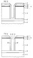
- An SOI substrate comprises a monocrystalline silicon wafer 1, which is p+-doped, for example, an insulating layer 2 made of SiO 2 arranged thereon and a monocrystalline silicon layer 3 arranged thereon (see FIG. 1).
- the SOI substrate is preferably produced by the direct wafer bonding (DWB) or silicon direct bonding (SDB) method, which is known, for example, from Yu Ohata et al, IEEE 1987, pp. 443-446.
- the thickness of the insulating layer 2 is, for example, 2 ⁇ m.
- the thickness of the monocrystalline silicon layer 3 is, for example, 20 ⁇ m.
- the monocrystalline silicon layer 3 is, for example, weakly n-doped.
- the dopant concentration in the monocrystalline silicon layer 3 is, for example, 1014 phosphorus atoms / cm 3. The components are later produced in the monocrystalline silicon layer 3.
- a trench mask 4 is applied to the surface of the monocrystalline silicon layer 3.
- the trench mask 4 comprises a lower layer 41, a middle layer 42 and an upper layer 43.
- the lower layer 41 is produced, for example, by thermal oxidation in a thickness of 50 nm.
- the middle layer 42 is produced for example by CVD deposition of Si3N3 in a thickness of 150 nm.
- the upper layer 43 is produced for example by CVD deposition of SiO2 in a thickness of 1600 nm.
- a resist mask 5 is applied to this layer sequence.
- the trench mask 4 is structured using the resist mask 5 in a CHF3 / O2 dry etching process.
- the trench mask must be suitable for etching a deep trench.
- a trench 6 is etched into the monocrystalline silicon layer 3 with the aid of the trench mask 4 (see FIG. 2).
- the etching takes place, for example, anisotropically in a dry etching process with a Cl2 / O2 chemistry.
- the etching is selective to SiO2. Therefore, the etching stops as soon as the surface of the insulating layer 2 is exposed.
- etching products located on the side walls are removed in an HF dip.
- a doped silicon layer 7 is deposited on the surface of the trench mask 4, the side walls 61 of the trench and the exposed surface of the insulating layer 2 (see FIG. 3).
- the doped silicon layer 7 is doped in situ.
- the doped silicon layer 7 consists for example of amorphous silicon and has a dopant concentration of for example 4. 1020 cm ⁇ 3 boron.
- the doped silicon layer 7 is deposited at 400 to 550 ° C.
- the dopant is embedded in the amorphous silicon, but is not yet activated.
- the doped silicon layer 7 is deposited with an essentially conformal edge covering. This means that the layer thickness of the doped silicon layer 7 on horizontal and on vertical substrates is essentially the same.
- the thickness of the doped silicon layer 7 is matched to the width and the geometry of the trench 6. With a width of the trench 6 of, for example, 2 ⁇ m, the doped silicon layer 7 is deposited, for example, in a thickness of 400 nm.
- the coating layer is made of borosilicate glass or phosphorus silicate glass by atmospheric CVD deposition (APCVD).
- the dopant content in the coating layer is 1 to 8 percent by weight, preferably 4 to 6 percent by weight.
- a tempering step at, for example, 1000 ° C. in a nitrogen atmosphere for 20 minutes, the dopant is diffused out of the covering layer, so that a doped silicon layer 7 is formed from the undoped silicon layer.
- any fluctuations in the thickness of the covering layer do not lead to nonuniformities in the doping in the doped silicon layer 7, since a uniform dopant concentration is established in the doped silicon layer 7 due to the diffusion in silicon.
- the covering layer is removed selectively with respect to the doped silicon layer 7 by means of dry and / or wet etching.
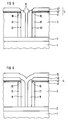
- the doped silicon layer 7 is etched until horizontal surfaces of the trench mask 4 and the insulating layer 2 are exposed (see FIG. 4). This creates 6 spacers 8 made of doped silicon on the side walls 61 of the trench.
- the spacers 8 made of doped silicon can also be deposited by selective epitaxy.
- silicon only grows on exposed silicon surfaces. Since the horizontal surface of the trench mask 4 and the insulating layer 2 consists of SiO2 and the surface of the monocrystalline silicon layer 3 is only exposed on the side walls 61 of the trench 6, the spacers grow 8 in the case of selective epitaxy only on the side walls 61 of the trench 6.
- the selective epitaxy is carried out, for example, using a mixture of Cl2 and SiH4.
- the process gas is added as a doping gas in N2 diluted B2H6 to dope the spacer 8 in situ with, for example, 4 x 1020 cm ⁇ 3 boron.
- the spacers 8 are to be n-doped, AsH3 diluted in N2 is suitable as the doping gas.
- the selective epitaxy is carried out, for example, in the temperature range between 800 ° C and 900 ° C and at a pressure of 500 mTorr - 100 Torr.
- dopant diffuses from the spacers 8 into the monocrystalline silicon layer 3 and forms diffusion regions 11 there, adjacent to the trench 6 (see FIG. 5).
- the amorphous silicon of the spacers 8 is partially recrystallized. This forms an insulation structure 9 and an SiO2 bird's beak 10 at the upper edge of the monocrystalline silicon layer 3.
- the temperature treatment is continued at least until the oxide thickness required for insulation is reached.
- the SiO2 bird's beak 10 is formed by oxidation of silicon in the monocrystalline silicon layer 3.
- the insulation structure 9 is formed by oxidation of silicon in the spacer 8.
- the dopant concentration in the diffusion region 11 is established depending on the doping of the spacer 8.
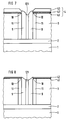
- the remaining free space in the trench 6 is filled by depositing a further silicon layer 12 (see FIG. 6).
- the further silicon layer 12 consists, for example, of amorphous silicon (see FIG. 6).
- the surface of the upper layer 43 of the trench mask 4 is exposed.
- Amorphous silicon of the further silicon layer 12 remaining in the free space of the trench 6 forms a silicon filling 121 (see FIG. 7). The etching is continued until the upper edge of the silicon fill 121 closes below the lower layer 41 made of thermal SiO 2 of the trench mask 4.
- the upper layer 43 of the trench mask 4 is removed by etching with, for example, CHF3 / O2 (see FIG. 8).
- the etching is selective to Si3N4, so that it stops on the surface of the middle layer 42 of the trench mask 4.
- the insulation structure 9, which also consists of SiO2 is etched back in the upper region, so that the insulation structure 9 then closes approximately in height with the middle layer 42 of the trench mask 4.
- the surface of the silicon filling 121 is oxidized. This creates an insulation termination 13 which completely covers the silicon filling 121.
- the insulation termination 13 is created without the use of a mask technique, that is to say self-adjusted. Simultaneously with the formation of the insulation termination 13, the SiO2 bird's beak 10 continues to form at the upper edge of the monocrystalline silicon layer 13. By rounding the edges, it contributes to increasing the breakdown voltage.
- the free space remaining within the insulation structure 9 can be filled in as an alternative to the method described with reference to FIGS. 6 to 9 by conformal deposition of SiO2, for example in an O3 / TEOS method.
- a CVD process is carried out in which a process gas containing O3 and Si (OC2H5) 4 is used.
- the CVD process is carried out, for example, at a pressure in the range from 50 to 600 torr and a temperature in the range from 200 to 600 ° C.
- the proportion of O3 in the process gas is 0.5 - 6 percent by weight.
- the remaining space in the trench is completely filled with SiO2.
- the logic components and the high-voltage components are then produced in the monocrystalline silicon layer 3.
- FIG. 10 shows the boron distribution of a boron-doped silicon layer arranged on a substrate.
- the dashed line O1 indicates the surface of the silicon substrate.
- the silicon substrate is doped with 1015 phosphorus atoms per cm3.
- the boron-doped silicon layer has a thickness of 500 nm and is doped with 4 x 1020cm ⁇ 3 boron.
- the region corresponding to the doped silicon layer is denoted by S1 and the region corresponding to the substrate by S2.
- the boron dope concentration shows a steep decrease in the area O 1 of the substrate S 2.
- FIG. 11 shows the boron distribution after outdiffusion and oxidation of the doped silicon layer in a humid atmosphere at 1000 ° C.
- a SiO2 layer which corresponds to the area labeled S3 in Figure 11 corresponds.
- a p-doped diffusion region is formed in the surface of the substrate by outdiffusion.
- the diffusion area corresponds to the area designated S..
- the initial doping of the substrate predominates in the region designated by Sd in FIG.
- the dashed line labeled O2 in Figure 11 corresponds to the surface of the substrate.
- the dashed line labeled O3 in Figure 11 corresponds to the boundary of the diffusion area.
- FIG. 10 and FIG. 11 are the result of simulation calculations, with which it was verified that, at 1000 ° C. in a humid atmosphere, both a complete oxidation of an amorphous silicon layer and the outdiffusion and formation of the diffusion area are possible.
- Another advantage of the method according to the invention is that the process steps for doping the side wall of the trench and for filling the trench are conventional process steps from CMOS technology. Since such CMOS processes are required in any case for the production of the logic components, this means that only steps compatible with CMOS processes are used.
Landscapes
- Element Separation (AREA)
Applications Claiming Priority (2)
| Application Number | Priority Date | Filing Date | Title |
|---|---|---|---|
| DE4320885 | 1993-06-23 | ||
| DE4320885 | 1993-06-23 |
Publications (2)
| Publication Number | Publication Date |
|---|---|
| EP0631306A1 true EP0631306A1 (fr) | 1994-12-28 |
| EP0631306B1 EP0631306B1 (fr) | 2000-04-26 |
Family
ID=6491041
Family Applications (1)
| Application Number | Title | Priority Date | Filing Date |
|---|---|---|---|
| EP94108804A Expired - Lifetime EP0631306B1 (fr) | 1993-06-23 | 1994-06-08 | Procédé de fabrication d'une région d'isolation dans un substrat pour la technologie de puissance intélligente |
Country Status (4)
| Country | Link |
|---|---|
| US (1) | US5700712A (fr) |
| EP (1) | EP0631306B1 (fr) |
| JP (1) | JPH0799241A (fr) |
| DE (1) | DE59409300D1 (fr) |
Cited By (3)
| Publication number | Priority date | Publication date | Assignee | Title |
|---|---|---|---|---|
| DE19728282A1 (de) * | 1997-07-02 | 1999-01-07 | Siemens Ag | Herstellverfahren für einen Isolationsgraben in einem SOI-Substrat |
| DE10234165A1 (de) * | 2002-07-26 | 2004-02-12 | Advanced Micro Devices, Inc., Sunnyvale | Verfahren zum Füllen einer in einer Materialschicht gebildeten Öffnung mit einem isolierenden Material |
| EP2317555A3 (fr) * | 2008-03-27 | 2013-03-13 | Hitachi, Ltd. | Dispositif de semi-conducteurs et son procédé de fabrication |
Families Citing this family (46)
| Publication number | Priority date | Publication date | Assignee | Title |
|---|---|---|---|---|
| JPH09172061A (ja) * | 1995-12-18 | 1997-06-30 | Fuji Electric Co Ltd | 半導体装置の製造方法 |
| US5933746A (en) * | 1996-04-23 | 1999-08-03 | Harris Corporation | Process of forming trench isolation device |
| US6025220A (en) | 1996-06-18 | 2000-02-15 | Micron Technology, Inc. | Method of forming a polysilicon diode and devices incorporating such diode |
| JP3353644B2 (ja) * | 1997-04-24 | 2002-12-03 | 日本電気株式会社 | プロセスシミュレーション方法 |
| KR100519834B1 (ko) * | 1997-05-29 | 2005-10-06 | 코닌클리즈케 필립스 일렉트로닉스 엔.브이. | 전자 디바이스의 제조 방법 |
| US6153478A (en) * | 1998-01-28 | 2000-11-28 | United Microelectronics Corp. | STI process for eliminating kink effect |
| DE19816449C2 (de) | 1998-04-14 | 2000-10-26 | Siemens Ag | Verfahren zum Herstellen eines SOI-Wafers für niederohmige Hochvolt-Halbleiterbauelemente |
| FR2785087B1 (fr) * | 1998-10-23 | 2003-01-03 | St Microelectronics Sa | Procede de formation dans une plaquette de silicium d'un caisson isole |
| US6191447B1 (en) | 1999-05-28 | 2001-02-20 | Micro-Ohm Corporation | Power semiconductor devices that utilize tapered trench-based insulating regions to improve electric field profiles in highly doped drift region mesas and methods of forming same |
| GB9915589D0 (en) * | 1999-07-02 | 1999-09-01 | Smithkline Beecham Plc | Novel compounds |
| GB9929613D0 (en) * | 1999-12-15 | 2000-02-09 | Koninkl Philips Electronics Nv | Manufacture of semiconductor material and devices using that material |
| US6506657B1 (en) * | 2000-04-19 | 2003-01-14 | National Semiconductor Corporation | Process for forming damascene-type isolation structure for BJT device formed in trench |
| US6627949B2 (en) * | 2000-06-02 | 2003-09-30 | General Semiconductor, Inc. | High voltage power MOSFET having low on-resistance |
| US6479352B2 (en) * | 2000-06-02 | 2002-11-12 | General Semiconductor, Inc. | Method of fabricating high voltage power MOSFET having low on-resistance |
| KR100419869B1 (ko) * | 2000-08-02 | 2004-02-25 | 주식회사 하이닉스반도체 | 쉘로우트렌치분리 형성방법 |
| KR20020051351A (ko) * | 2000-12-22 | 2002-06-29 | 박종섭 | 반도체장치의 소자격리방법 |
| US6436791B1 (en) | 2001-06-14 | 2002-08-20 | Taiwan Semiconductor Manufacturing Company | Method of manufacturing a very deep STI (shallow trench isolation) |
| DE10148491B4 (de) * | 2001-10-01 | 2006-09-07 | Infineon Technologies Ag | Verfahren zum Herstellen einer integrierten Halbleiteranordnung mit Hilfe einer thermischen Oxidation und Halbleiteranordnung |
| US6576516B1 (en) * | 2001-12-31 | 2003-06-10 | General Semiconductor, Inc. | High voltage power MOSFET having a voltage sustaining region that includes doped columns formed by trench etching and diffusion from regions of oppositely doped polysilicon |
| JP2004047624A (ja) * | 2002-07-10 | 2004-02-12 | Renesas Technology Corp | 半導体装置およびその製造方法 |
| US6627502B1 (en) * | 2002-10-24 | 2003-09-30 | Taiwan Semiconductor Manufacturing Company | Method for forming high concentration shallow junctions for short channel MOSFETs |
| US7238588B2 (en) * | 2003-01-14 | 2007-07-03 | Advanced Micro Devices, Inc. | Silicon buffered shallow trench isolation |
| US7648886B2 (en) * | 2003-01-14 | 2010-01-19 | Globalfoundries Inc. | Shallow trench isolation process |
| US6962857B1 (en) | 2003-02-05 | 2005-11-08 | Advanced Micro Devices, Inc. | Shallow trench isolation process using oxide deposition and anneal |
| US7422961B2 (en) * | 2003-03-14 | 2008-09-09 | Advanced Micro Devices, Inc. | Method of forming isolation regions for integrated circuits |
| TWI230432B (en) * | 2003-05-05 | 2005-04-01 | Nanya Technology Corp | Method for improving sneakage at shallow trench isolation and STI structure thereof |
| US6921709B1 (en) | 2003-07-15 | 2005-07-26 | Advanced Micro Devices, Inc. | Front side seal to prevent germanium outgassing |
| US7462549B2 (en) * | 2004-01-12 | 2008-12-09 | Advanced Micro Devices, Inc. | Shallow trench isolation process and structure with minimized strained silicon consumption |
| US7183610B2 (en) * | 2004-04-30 | 2007-02-27 | Siliconix Incorporated | Super trench MOSFET including buried source electrode and method of fabricating the same |
| ITTO20050056A1 (it) * | 2005-02-03 | 2006-08-04 | St Microelectronics Srl | Procedimento di fabbricazione di una fetta soi con aumentata capacita' di segregazione delle impurita' |
| US7553740B2 (en) | 2005-05-26 | 2009-06-30 | Fairchild Semiconductor Corporation | Structure and method for forming a minimum pitch trench-gate FET with heavy body region |
| US7723204B2 (en) * | 2006-03-27 | 2010-05-25 | Freescale Semiconductor, Inc. | Semiconductor device with a multi-plate isolation structure |
| US8153502B2 (en) * | 2006-05-16 | 2012-04-10 | Micron Technology, Inc. | Methods for filling trenches in a semiconductor material |
| KR100869742B1 (ko) * | 2006-12-29 | 2008-11-21 | 동부일렉트로닉스 주식회사 | 반도체 소자의 소자 분리막 형성 방법 |
| US7786535B2 (en) * | 2008-01-11 | 2010-08-31 | International Business Machines Corporation | Design structures for high-voltage integrated circuits |
| US7772651B2 (en) * | 2008-01-11 | 2010-08-10 | International Business Machines Corporation | Semiconductor-on-insulator high-voltage device structures, methods of fabricating such device structures, and design structures for high-voltage circuits |
| US7790543B2 (en) * | 2008-01-11 | 2010-09-07 | International Business Machines Corporation | Device structures for a metal-oxide-semiconductor field effect transistor and methods of fabricating such device structures |
| US7790524B2 (en) * | 2008-01-11 | 2010-09-07 | International Business Machines Corporation | Device and design structures for memory cells in a non-volatile random access memory and methods of fabricating such device structures |
| US7700428B2 (en) * | 2008-05-09 | 2010-04-20 | International Business Machines Corporation | Methods of fabricating a device structure for use as a memory cell in a non-volatile random access memory |
| US7804124B2 (en) * | 2008-05-09 | 2010-09-28 | International Business Machines Corporation | Device structures for a memory cell of a non-volatile random access memory and design structures for a non-volatile random access memory |
| US9578128B2 (en) * | 2012-10-29 | 2017-02-21 | Google Inc. | Systems and methods for message delivery to mobile devices supporting multiple users |
| JP6059085B2 (ja) * | 2013-05-27 | 2017-01-11 | 東京エレクトロン株式会社 | トレンチを充填する方法及び処理装置 |
| KR102318197B1 (ko) | 2014-09-22 | 2021-10-26 | 삼성전자주식회사 | 씨모스 이미지 센서의 픽셀 및 이를 포함하는 이미지 센서 |
| CN109643639B (zh) * | 2016-09-13 | 2023-08-11 | 应用材料公司 | 用于间隔件和硬掩模应用的硼烷介导的从硅烷和烷基硅烷物质脱氢的工艺 |
| US10707330B2 (en) | 2018-02-15 | 2020-07-07 | Globalfoundries Inc. | Semiconductor device with interconnect to source/drain |
| WO2023140838A1 (fr) * | 2022-01-20 | 2023-07-27 | Applied Materials, Inc. | Procédés de formation de structures d'isolation de tranchée profonde |
Citations (6)
| Publication number | Priority date | Publication date | Assignee | Title |
|---|---|---|---|---|
| WO1985004760A1 (fr) * | 1984-04-05 | 1985-10-24 | American Telephone & Telegraph Company | Procede de dopage regule des parois laterales d'une tranchee dans un corps de semi-conducteur |
| WO1986004454A1 (fr) * | 1985-01-25 | 1986-07-31 | American Telephone & Telegraph Company | Dopage regule du silicium par du bore |
| US4666556A (en) * | 1986-05-12 | 1987-05-19 | International Business Machines Corporation | Trench sidewall isolation by polysilicon oxidation |
| EP0265958A2 (fr) * | 1986-10-30 | 1988-05-04 | SGS Microelettronica SpA | Procédé pour faire des transistors à effet de champ à porte isolée |
| EP0295786A2 (fr) * | 1987-06-15 | 1988-12-21 | DELCO ELECTRONICS CORPORATION (a Delaware corp.) | Procédé pour faire croître des plaquettes de silicium-sur-isolant |
| EP0296754A2 (fr) * | 1987-06-18 | 1988-12-28 | Kabushiki Kaisha Toshiba | Procédé de fabrication de dispositifs semi-conducteurs ayant des régions d'isolation comportant des rainures |
Family Cites Families (16)
| Publication number | Priority date | Publication date | Assignee | Title |
|---|---|---|---|---|
| DE2449688C3 (de) * | 1974-10-18 | 1980-07-10 | Siemens Ag, 1000 Berlin Und 8000 Muenchen | Verfahren zur Herstellung einer dotierten Zone eines Leitfähigkeitstyps in einem Halbleiterkörper |
| US4274892A (en) * | 1978-12-14 | 1981-06-23 | Trw Inc. | Dopant diffusion method of making semiconductor products |
| US4333794A (en) * | 1981-04-07 | 1982-06-08 | International Business Machines Corporation | Omission of thick Si3 N4 layers in ISA schemes |
| US4473598A (en) * | 1982-06-30 | 1984-09-25 | International Business Machines Corporation | Method of filling trenches with silicon and structures |
| US4861729A (en) * | 1987-08-24 | 1989-08-29 | Matsushita Electric Industrial Co., Ltd. | Method of doping impurities into sidewall of trench by use of plasma source |
| US4847214A (en) * | 1988-04-18 | 1989-07-11 | Motorola Inc. | Method for filling trenches from a seed layer |
| KR910005401B1 (ko) * | 1988-09-07 | 1991-07-29 | 경상현 | 비결정 실리콘을 이용한 자기정렬 트랜지스터 제조방법 |
| JP3130906B2 (ja) * | 1989-12-01 | 2001-01-31 | セイコーインスツルメンツ株式会社 | 半導体内壁に対する不純物の注入方法 |
| US5116778A (en) * | 1990-02-05 | 1992-05-26 | Advanced Micro Devices, Inc. | Dopant sources for cmos device |
| JP2597022B2 (ja) * | 1990-02-23 | 1997-04-02 | シャープ株式会社 | 素子分離領域の形成方法 |
| EP0469555B1 (fr) * | 1990-07-31 | 1996-04-17 | Nec Corporation | Electrode à stockage de charges d'une capacité et sa méthode de fabrication |
| KR100209856B1 (ko) * | 1990-08-31 | 1999-07-15 | 가나이 쓰도무 | 반도체장치의 제조방법 |
| KR920020676A (ko) * | 1991-04-09 | 1992-11-21 | 김광호 | 반도체 장치의 소자분리 방법 |
| US5192708A (en) * | 1991-04-29 | 1993-03-09 | International Business Machines Corporation | Sub-layer contact technique using in situ doped amorphous silicon and solid phase recrystallization |
| JPH05234900A (ja) * | 1992-02-19 | 1993-09-10 | Nec Corp | 半導体装置の製造方法 |
| US5416041A (en) * | 1993-09-27 | 1995-05-16 | Siemens Aktiengesellschaft | Method for producing an insulating trench in an SOI substrate |
-
1994
- 1994-06-08 DE DE59409300T patent/DE59409300D1/de not_active Expired - Fee Related
- 1994-06-08 EP EP94108804A patent/EP0631306B1/fr not_active Expired - Lifetime
- 1994-06-20 JP JP6160625A patent/JPH0799241A/ja active Pending
-
1995
- 1995-11-03 US US08/552,976 patent/US5700712A/en not_active Expired - Fee Related
Patent Citations (6)
| Publication number | Priority date | Publication date | Assignee | Title |
|---|---|---|---|---|
| WO1985004760A1 (fr) * | 1984-04-05 | 1985-10-24 | American Telephone & Telegraph Company | Procede de dopage regule des parois laterales d'une tranchee dans un corps de semi-conducteur |
| WO1986004454A1 (fr) * | 1985-01-25 | 1986-07-31 | American Telephone & Telegraph Company | Dopage regule du silicium par du bore |
| US4666556A (en) * | 1986-05-12 | 1987-05-19 | International Business Machines Corporation | Trench sidewall isolation by polysilicon oxidation |
| EP0265958A2 (fr) * | 1986-10-30 | 1988-05-04 | SGS Microelettronica SpA | Procédé pour faire des transistors à effet de champ à porte isolée |
| EP0295786A2 (fr) * | 1987-06-15 | 1988-12-21 | DELCO ELECTRONICS CORPORATION (a Delaware corp.) | Procédé pour faire croître des plaquettes de silicium-sur-isolant |
| EP0296754A2 (fr) * | 1987-06-18 | 1988-12-28 | Kabushiki Kaisha Toshiba | Procédé de fabrication de dispositifs semi-conducteurs ayant des régions d'isolation comportant des rainures |
Non-Patent Citations (3)
| Title |
|---|
| "SIDEWALL CHANNEL-STOP DOPING FOR DEEP-TRENCH ISOLATION OF FET DEVICES", IBM TECHNICAL DISCLOSURE BULLETIN., vol. 27, no. 10A, March 1985 (1985-03-01), NEW YORK US, pages 5501 - 5504 * |
| A. NAKAGAWA ET AL.: "500 V LATERAL DOUBLE GATE BIPOLAR-MODE MOSFET(DGIGBT) DIELECTRICALLY ISOLATED BY SILICON WAFER DIRECT-BONDING (DISDB)", EXTENDED ABSTRACTS OF THE 20TH (1988 INTERNATIONAL ) CONFERENCE ON SOLID STATE DEVICES ANS MATERIALS TOKYO 1988, 1988, TOKYO, pages 33 - 36 * |
| K. FUJINO ET AL.: "SURFACE MODIFICATION OF BASE MATERIALS FOR TEOS/O3 ATMOSPHERIC PRESSURE CHEMICAL VAPOR DEPOSITION.", JOURNAL OF THE ELECTROCHEMICAL SOCIETY, vol. 139, no. 6, June 1992 (1992-06-01), MANCHESTER, NEW HAMPSHIRE US, pages 1690 - 1692, XP000324421 * |
Cited By (5)
| Publication number | Priority date | Publication date | Assignee | Title |
|---|---|---|---|---|
| DE19728282A1 (de) * | 1997-07-02 | 1999-01-07 | Siemens Ag | Herstellverfahren für einen Isolationsgraben in einem SOI-Substrat |
| DE10234165A1 (de) * | 2002-07-26 | 2004-02-12 | Advanced Micro Devices, Inc., Sunnyvale | Verfahren zum Füllen einer in einer Materialschicht gebildeten Öffnung mit einem isolierenden Material |
| US6812115B2 (en) | 2002-07-26 | 2004-11-02 | Advanced Micro Devices, Inc. | Method of filling an opening in a material layer with an insulating material |
| DE10234165B4 (de) * | 2002-07-26 | 2008-01-03 | Advanced Micro Devices, Inc., Sunnyvale | Verfahren zum Füllen eines Grabens, der in einem Substrat gebildet ist, mit einem isolierenden Material |
| EP2317555A3 (fr) * | 2008-03-27 | 2013-03-13 | Hitachi, Ltd. | Dispositif de semi-conducteurs et son procédé de fabrication |
Also Published As
| Publication number | Publication date |
|---|---|
| US5700712A (en) | 1997-12-23 |
| EP0631306B1 (fr) | 2000-04-26 |
| JPH0799241A (ja) | 1995-04-11 |
| DE59409300D1 (de) | 2000-05-31 |
Similar Documents
| Publication | Publication Date | Title |
|---|---|---|
| EP0631306B1 (fr) | Procédé de fabrication d'une région d'isolation dans un substrat pour la technologie de puissance intélligente | |
| EP0631305B1 (fr) | Procédé de fabrication d'une région d'isolation dans un substrat pour la technologie de puissance intélligente | |
| EP0645808B1 (fr) | Procédé de fabrication d'une rainure d'isolation dans un substrat du type SOI | |
| DE3784958T2 (de) | Seitenwanddistanzschichten zur Spannungsaufnahme und Isolierung von CMOS Schaltungen und Herstellungsverfahren. | |
| EP0635884A1 (fr) | Procédé pour la fabrication d'une rainure dans un substrat et application à la technologie de puissance vive | |
| DE19906030B4 (de) | Grabenisolationsstruktur eines Halbleiterbauteils und Verfahren zum Herstellen einer Grabenisolationsstruktur mit Polysiliziumkontakt | |
| DE4310954C2 (de) | Halbleiter-Bearbeitungsverfahren zum Herstellen eines Isoliergrabens in einem Substrat | |
| DE3686453T2 (de) | Verfahren zum herstellen einer duennen halbleiterschicht. | |
| DE19909993B4 (de) | Verfahren zum Bilden von Bipolartransistoren mit selbstausrichtender epitaktischer Basis | |
| DE3129558C2 (fr) | ||
| DE19961085A1 (de) | Verfahren zum Herstellen einer Tiefgrabenspeicherelektrode eines Kondensators | |
| DE4404757C2 (de) | Verfahren zur Herstellung eines einem Graben benachbarten Diffusionsgebietes in einem Substrat | |
| DE10324433B4 (de) | Verfahren zur Herstellung eines Substratkontakts für ein SOI-Halbleiterbauteil | |
| DE2510593C3 (de) | Integrierte Halbleiter-Schaltungsanordnung | |
| DE4211050C2 (de) | Verfahren zur Herstellung eines Bipolartransistors in einem Substrat | |
| DE4409875C2 (de) | Verfahren zur Herstellung eines MOS Transistors unter Verwendung einer doppelt dotierten Schicht | |
| EP0855088B1 (fr) | Procede de realisation d'une tranchee d'isolation dans un substrat | |
| DE19840385C2 (de) | Verfahren zm Isolieren von Bereichen eines integrierten Schaltkreises und Halbleiterbaustein mit integriertem Schaltkreis | |
| DE10261308A1 (de) | Bildung einer PBL-SiN-Barriere mit hohem Streckungsverhältnis | |
| DE4320062A1 (de) | Verfahren zum Isolieren einzelner Elemente in einem Halbleiterchip | |
| DE2738961A1 (de) | Verfahren zur herstellung einer integrierten halbleiterschaltung mit luftisolation | |
| DE4341180B4 (de) | Verfahren zur Isolation einer Halbleiterschicht auf einem Isolator zur Festlegung eines aktiven Gebiets | |
| EP0520214B1 (fr) | Méthode de formation d'une région dopée dans un substrat et application à la fabrication d'un transistor bipolaire | |
| EP0875931B1 (fr) | Procédé de fabrication d'un dispositif de circuit CMOS | |
| EP0517727B1 (fr) | Procede de production d'un ilot de silicium monocristallin isole |
Legal Events
| Date | Code | Title | Description |
|---|---|---|---|
| PUAI | Public reference made under article 153(3) epc to a published international application that has entered the european phase |
Free format text: ORIGINAL CODE: 0009012 |
|
| AK | Designated contracting states |
Kind code of ref document: A1 Designated state(s): DE FR GB IT |
|
| 17P | Request for examination filed |
Effective date: 19950428 |
|
| 17Q | First examination report despatched |
Effective date: 19950711 |
|
| GRAG | Despatch of communication of intention to grant |
Free format text: ORIGINAL CODE: EPIDOS AGRA |
|
| GRAG | Despatch of communication of intention to grant |
Free format text: ORIGINAL CODE: EPIDOS AGRA |
|
| GRAH | Despatch of communication of intention to grant a patent |
Free format text: ORIGINAL CODE: EPIDOS IGRA |
|
| GRAH | Despatch of communication of intention to grant a patent |
Free format text: ORIGINAL CODE: EPIDOS IGRA |
|
| GRAA | (expected) grant |
Free format text: ORIGINAL CODE: 0009210 |
|
| AK | Designated contracting states |
Kind code of ref document: B1 Designated state(s): DE FR GB IT |
|
| REF | Corresponds to: |
Ref document number: 59409300 Country of ref document: DE Date of ref document: 20000531 |
|
| ITF | It: translation for a ep patent filed | ||
| GBT | Gb: translation of ep patent filed (gb section 77(6)(a)/1977) |
Effective date: 20000629 |
|
| ET | Fr: translation filed | ||
| PLBE | No opposition filed within time limit |
Free format text: ORIGINAL CODE: 0009261 |
|
| STAA | Information on the status of an ep patent application or granted ep patent |
Free format text: STATUS: NO OPPOSITION FILED WITHIN TIME LIMIT |
|
| 26N | No opposition filed | ||
| PGFP | Annual fee paid to national office [announced via postgrant information from national office to epo] |
Ref country code: GB Payment date: 20010612 Year of fee payment: 8 |
|
| PGFP | Annual fee paid to national office [announced via postgrant information from national office to epo] |
Ref country code: FR Payment date: 20010622 Year of fee payment: 8 |
|
| PGFP | Annual fee paid to national office [announced via postgrant information from national office to epo] |
Ref country code: DE Payment date: 20010823 Year of fee payment: 8 |
|
| REG | Reference to a national code |
Ref country code: GB Ref legal event code: IF02 |
|
| PG25 | Lapsed in a contracting state [announced via postgrant information from national office to epo] |
Ref country code: GB Free format text: LAPSE BECAUSE OF NON-PAYMENT OF DUE FEES Effective date: 20020608 |
|
| PG25 | Lapsed in a contracting state [announced via postgrant information from national office to epo] |
Ref country code: DE Free format text: LAPSE BECAUSE OF NON-PAYMENT OF DUE FEES Effective date: 20030101 |
|
| GBPC | Gb: european patent ceased through non-payment of renewal fee |
Effective date: 20020608 |
|
| PG25 | Lapsed in a contracting state [announced via postgrant information from national office to epo] |
Ref country code: FR Free format text: LAPSE BECAUSE OF NON-PAYMENT OF DUE FEES Effective date: 20030228 |
|
| REG | Reference to a national code |
Ref country code: FR Ref legal event code: ST |
|
| PG25 | Lapsed in a contracting state [announced via postgrant information from national office to epo] |
Ref country code: IT Free format text: LAPSE BECAUSE OF NON-PAYMENT OF DUE FEES;WARNING: LAPSES OF ITALIAN PATENTS WITH EFFECTIVE DATE BEFORE 2007 MAY HAVE OCCURRED AT ANY TIME BEFORE 2007. THE CORRECT EFFECTIVE DATE MAY BE DIFFERENT FROM THE ONE RECORDED. Effective date: 20050608 |