EP0645809B1 - Procédé pour fabriquer un dispositif semi-conducteur comportant un corps semi-conducteur comportant des régions d'isolation de champ formées par des rainures remplies de matériau isolant - Google Patents
Procédé pour fabriquer un dispositif semi-conducteur comportant un corps semi-conducteur comportant des régions d'isolation de champ formées par des rainures remplies de matériau isolant Download PDFInfo
- Publication number
- EP0645809B1 EP0645809B1 EP94202660A EP94202660A EP0645809B1 EP 0645809 B1 EP0645809 B1 EP 0645809B1 EP 94202660 A EP94202660 A EP 94202660A EP 94202660 A EP94202660 A EP 94202660A EP 0645809 B1 EP0645809 B1 EP 0645809B1
- Authority
- EP
- European Patent Office
- Prior art keywords
- semiconductor body
- auxiliary layer
- etching mask
- layer
- grooves
- Prior art date
- Legal status (The legal status is an assumption and is not a legal conclusion. Google has not performed a legal analysis and makes no representation as to the accuracy of the status listed.)
- Expired - Lifetime
Links
Images

Classifications
-
- H—ELECTRICITY
- H10—SEMICONDUCTOR DEVICES; ELECTRIC SOLID-STATE DEVICES NOT OTHERWISE PROVIDED FOR
- H10P—GENERIC PROCESSES OR APPARATUS FOR THE MANUFACTURE OR TREATMENT OF DEVICES COVERED BY CLASS H10
- H10P50/00—Etching of wafers, substrates or parts of devices
- H10P50/69—Etching of wafers, substrates or parts of devices using masks for semiconductor materials
- H10P50/691—Etching of wafers, substrates or parts of devices using masks for semiconductor materials for Group V materials or Group III-V materials
-
- H—ELECTRICITY
- H10—SEMICONDUCTOR DEVICES; ELECTRIC SOLID-STATE DEVICES NOT OTHERWISE PROVIDED FOR
- H10P—GENERIC PROCESSES OR APPARATUS FOR THE MANUFACTURE OR TREATMENT OF DEVICES COVERED BY CLASS H10
- H10P52/00—Grinding, lapping or polishing of wafers, substrates or parts of devices
- H10P52/40—Chemomechanical polishing [CMP]
- H10P52/402—Chemomechanical polishing [CMP] of semiconductor materials
-
- H—ELECTRICITY
- H10—SEMICONDUCTOR DEVICES; ELECTRIC SOLID-STATE DEVICES NOT OTHERWISE PROVIDED FOR
- H10W—GENERIC PACKAGES, INTERCONNECTIONS, CONNECTORS OR OTHER CONSTRUCTIONAL DETAILS OF DEVICES COVERED BY CLASS H10
- H10W10/00—Isolation regions in semiconductor bodies between components of integrated devices
- H10W10/01—Manufacture or treatment
Definitions
- the invention relates to a method of manufacturing a semiconductor device comprising a semiconductor body with field insulation regions formed by grooves filled with insulating material, by which method the grooves are etched into the semiconductor body with the use of an etching mask formed on an auxiliary layer provided on a surface of the semiconductor body, the auxiliary layer is removed from the portion of the surface situated next to the etching mask and from an edge of the surface situated below the etching mask, and a layer of the insulating material is deposited on the semiconductor body, whereby the grooves are filled and the edge of the surface situated below the etching mask is covered, after which the semiconductor body is subjected to a treatment by which material is removed parallel to the surface down to said auxiliary layer and finally the remaining portion of the auxiliary layer is removed.
- Field insulation regions are thus formed which extend over an edge of active regions of the semiconductor body surrounded by the field insulation regions. These field insulation regions may be provided by processes in which no treatments at temperatures higher than 650 °C are required. Doping profiles already present in the semiconductor body, accordingly, are not interfered with by this method of providing the field oxide regions.
- Doped surface zones may subsequently be formed in the active regions of the semiconductor body surrounded by the field insulation regions.
- a layer of a doped semiconductor material is deposited on the semiconductor body then, after which the semiconductor body is subjected to a heat treatment whereby dopant diffuses from this layer into the semiconductor body. Since the edge of the active regions is covered by a strip of insulating material during this, it is prevented that dopants penetrate to an undesirable depth into the edge of the active regions during this heat treatment. This renders it impossible for pn junctions already present in the active regions to be short-circuited.
- JP-A-63/185043 discloses a method of the kind mentioned in the opening paragraph whereby the etching mask and the auxiliary layer are subjected to an isotropic etching treatment before the grooves are etched into the semiconductor body, which treatment is continued until the auxiliary layer has been removed both from the portion of the surface situated next to the etching mask and from the edge of the surface situated below the mask.
- the grooves are then etched into the semiconductor body in that the latter is subjected to an anisotropic etching treatment.
- a pattern of electric conductors may be applied on the active regions which were thus formed and surrounded by the field insulation regions.
- the semiconductor body is then covered with a layer of electrically conducting material which is subsequently provided with a photoresist mask corresponding to the pattern to be formed, after which the pattern is etched into the electrically conducting layer.
- the electric conductors formed interconnect inter alia doped surface zones. It is found in practice that short-circuits may occur in the pattern of electric conductors thus provided.
- JP-A-59-107534 discloses a method of manufacturing a semiconductor device comprising a semiconductor substrate with field isolation regions formed by grooves filled with insulating material.
- the grooves are filled using a lift-off method. After depositing the insulating material in the groove and on the masking layer, the masking layer is etched away whereby the silicon oxide layer on the masked layer is lifted off. The portion of the silicon oxide layer in the groove remains unchanged.
- the lift-off work can be done easily, because eaves are formed before the insulating material is deposited. The voids under the eaves however are not filled with insulating material.
- EP-A-0 166 141 and EP-A-0 542 647 disclose a method of manufacturing a semiconductor device comprising grooves filled with insulating material. In both cases however the grooves are etched and filled after the semiconductor zones have been formed. The problem of diffusion of dopants along the edges of the grooves during forming of semiconductor zones, for which the invention seeks a solution, thus will not occur in these known methods.
- US-A-5 236 861 and JP-A-5047920 disclose two different methods of forming field isolation regions which extend over an edge of the active regions surrounded by the field isolation regions.
- grooves are filled with insulating material by deposition and etch-back of a thick layer of silicon oxide. Then a selective thermal oxidation is carried out whereby said extensions of the field isolation regions are formed.
- JP-A-5047920 the grooves are etched in two successive steps. in the first step isotropic, in the second step anisotropic. Thus tapered grooves are formed which are provided with extensions at their upper side. The grooves with extensions are filled, so that the field isolation regions extend over an edged of the active regions.
- the invention has for its object inter alia to provide a method of manufacturing a semiconductor device comprising a semiconductor body with field insulation regions formed by grooves filled with insulating material, which grooves extend over an edge of the active regions of the semiconductor body surrounded by the field insulation regions, while the occurrence of short-circuits is counteracted in the formation of a pattern of electric conductors as described above.
- the method mentioned in the opening paragraph is for this purpose characterized in that the auxiliary layer is removed from the portion of the surface situated next to the etching mask before the grooves are etched into the semiconductor body, and in that the auxiliary layer is removed from the edge of the surface situated below the etching mask after the grooves have been etched into the semiconductor body.
- the auxiliary layer is etched isotropically until the auxiliary layer has been removed both from the portion of the surface situated next to the etching mask and from the edge of the surface situated below the mask.
- the auxiliary layer is etched from its upper side.
- the auxiliary layer is given a profile below the etching mask which encloses an acute angle with the surface of the semiconductor body.
- the strip of the field insulation regions which is deposited on the edge of the active regions lies against the auxiliary layer after the grooves have been filled.
- the strip exhibits an overhanging edge on the active regions after the removal of the remaining portion of the auxiliary layer.
- conducting tracks may be formed below this edge, which cause the short-circuits mentioned.
- the auxiliary layer is given a profile below the etchng mask which does not enclose an acute angle with the surface of the semiconductor body. The formation of conductor tracks which cause the said short-circuits is strongly counteracted thereby.
- a preferred embodiment of the method according to the invention is characterized in that the auxiliary layer is etched away anisotropically from the portion of the surface situated next to the etching mask, the grooves are subsequently etched anisotropically into the semiconductor body, and after that the auxiliary layer is etched away isotropically from the edge of the surface situated below the etching mask.
- the auxiliary layer is etched from its flat side which is exposed at that moment and is given a profile which is directed transversely to the surface of the semiconductor body.
- the strip of the field insulation regions, which is deposited on the edge of the active regions, as a result shows a substantially straight edge on the active regions after removal of the auxiliary layer.
- the formation of the conductor tracks which cause the said short-circuits is strongly counteracted thereby.
- the active regions have dimensions which are practically identical to those of the etching mask in this embodiment of the method.
- auxiliary layer is etched away anisotropically from the portion of the surface situated next to the etching mask, the grooves are subsequently etched isotropically into the semiconductor body, and the auxiliary layer is then etched away isotropically from the edge of the surface situated below the etching mask.
- the grooves etched in this manner extend to below the auxiliary layer.
- the auxiliary layer is then in fact etched away from the etching mask, the active region being used as a mask.
- the auxiliary layer accordingly gets a profile which encloses an obtuse angle with the surface of the semiconductor body, and the field insulation regions are given a strip situated on the active regions and having a profile which encloses an acute angle with the surface.
- the formation of conductor tracks which cause the said short-circuits has become practically impossible as a result.
- the active regions have dimensions smaller than those of the etching mask. This should accordingly be taken into account in the design of semiconductor devices manufactured by this embodiment of the method.
- the etched grooves may be filled with insulating material in that a layer of this material is provided to such a depth that it has a substantially plane surface, upon which an etching treatment is carried out.
- the layer of insulating material then has a surface which runs practically parallel to the surface of the device, and a material reduction which proceeds parallel to the surface is obtained by the etching treatment. If a thinner layer of insulating material is provided, it will have a surface which more or less follows the etched grooves. In that case a photoresist layer may be provided on the layer of insulating material to such a thickness that it shows a practically plane surface.
- the semiconductor body is subjected to a chemical-mechanical polishing treatment after the deposition of the layer of insulating material, by which treatment the insulating material and the subjacent etching mask are taken off parallel to the surface down to said auxiliary layer.
- a chemical-mechanical polishing treatment it is immaterial whether the layer of insulating material itself has a comparatively plane surface or not. The layer of insulating material need not be provided to a comparatively great thickness, and a photoresist layer is unnecessary.
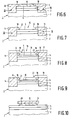
- Figs. 1 to 8 diagrammatically and in cross-section show a number of stages in the manufacture of a semiconductor device comprising a semiconductor body 1 with field insulation regions 14 formed by grooves 10 filled with insulating material 13.
- the semiconductor 1 in this example is provided with a surface layer 2 of n-type doped silicon with a doping concentration of 10 20 atoms per cc, provided with an n-type epitaxially grown, approximately 0.3 ⁇ m thick n-type layer 3 with a doping concentration of 10 17 atoms per cc.
- An approximately 0.1 ⁇ m thick p-type surface zone 4 with a doping concentration of 3.10 18 atoms per cc has already been provided in this layer 3 in a usual manner.
- a layer of, for example, p-type Si 1-x Ge x with 0.1 ⁇ x ⁇ 0.5 may alternatively be grown epitaxially on the layer 3.
- An approximately 0.15 ⁇ m thick auxiliary layer 6 of silicon nitride and an approximately 0.2 ⁇ m thick masking layer 7 of silicon oxide are deposited on a surface 5 of the semiconductor body 1.
- An approximately 20 nm thick layer of silicon oxide (not shown) may be provided below the auxiliary layer 6.
- a photoresist mask 8 is provided in usual manner on the auxiliary layer 6, with which mask an etching mask 9 is etched into the masking layer 7. Grooves 10 are etched into the semiconductor body 1 with the use of the etching mask 9 which is formed on the auxiliary layer 6 provided on the surface 5 of the semiconductor body 1.
- the auxiliary layer 6 is removed from the portion 11 of the surface 5 situated next to the etching mask 8 and from an edge 12 of the surface 5 situated below the etching mask 8. Then a layer 13 of the insulating material with which the grooves 10 are to be filled is deposited on the semiconductor body 1. The grooves 10 are filled thereby and the edge 12 of the surface 5 situated below the etching mask 9 is covered. As is shown in Figs. 5 and 6, the semiconductor body 1 is then subjected to a treatment by which material is taken off parallel to the surface 5 down to said auxiliary layer 6, and finally the remaining portion of the auxiliary layer 6 is eliminated.
- Field insulation regions 14 are thus formed, extending over the edge 12 of active regions 15 of the semiconductor body 1 surrounded by the field insulation regions 14.
- These field insulation regions 14 may he provided in usual manner by processes in which no treatments at a temperature higher than 650 °C are required. Doping profiles of the epitaxially grown layer 3 and the surface zone 4 already present in the semiconductor body 1 are accordingly not interfered with by the creation of the field oxide regions.
- Doped surface zones 16 are subsequently formed in the active regions 15 of the semiconductor body surrounded by the field insulation regions 14.
- a layer 17 of n-type doped polycrystalline silicon with a doping of 10 21 atoms per cc is deposited on the semiconductor body 1, after which the semiconductor body 1 is subjected to a heat treatment whereby dopant diffuses from this layer into the semiconductor body. Since the edge 12 of the active regions 15 is covered by a strip of insulating material 18 during this, it is prevented that dopant penetrates to an undesirable depth into the edge 12 of the active regions 15 during this heat treatment. Thus it is prevented that the surface zone 16 and the epitaxially grown layer 3 are interconnected in the active regions 15, whereby any pn junctions present between the layers 16, 4 and 3 would be short-circuited.
- a pattern of electric conductors can be provided on the active regions 15 thus formed and surrounded by the field insulation regions 14. In this case this would refer to the layer of n-type doped polycrystalline silicon 17. It would be alternatively possible, however, to cover the semiconductor body 1 with a layer of a different electrically conducting material after removal of the layer 17.
- the layer 14 is provided with a photoresist mask (not shown) corresponding to the pattern to be formed, after which the conductors 19 are etched into the layer of polycrystalline silicon 17.
- the electric conductors formed interconnect inter alia doped surface zones 16 across the field oxide regions 14.
- the auxiliary layer 6 is removed from the portion 11 of the surface 5 situated next to the etchng mask 9 before the grooves 10 are etched into the semiconductor body, and the auxiliary layer 6 is removed from the edge 12 of the surface 15 situated below the etching mask 9 after the grooves 10 have been etched into the semiconductor body 1.
- the occurrence of short-circuits in the pattern of electric conductors 19 extending over the field insulation regions 14 and the active regions 15 is strongly counteracted thereby.
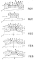
- auxiliary layer 6 were etched away both from the portion 11 of the surface 5 situated next to the etching mask 9 and from the edge 12 of the surface 5 situated below the mask 9 before the grooves 10 are etched, then the auxiliary layer 6 would be etched from its upper side during this etching treatment, which may be carried out equally well with an etching liquid and with an etching plasma.
- the auxiliary layer 6 would then be given a profile which encloses an acute angle 20 with the surface 5 of the semiconductor body 1 below the etching mask 6, as indicated diagrammatically in Fig. 10.
- the strip of the field insulation regions 14 deposited on the edge 12 of the active regions will lie against the auxiliary layer 6 after filling of the grooves 10.
- the strip 18 accordingly has an overhanging edge 21 on the active regions 15 after the removal of the remaining portion of the auxiliary layer 6.
- conductor tracks 21 may be formed below this edge 21, which may cause short-circuits between various conductor tracks 19.
- the auxiliary layer 9 is given a profile which does not enclose an acute angle with the surface 5 of the semiconductor body 1 below the etching mask 9, as is indicated diagrammatically in Figs. 5 and 13. The formation of conductor tracks which cause the said short-circuits is strongly counteracted thereby.
- the auxiliary layer 6 is etched away anisotropically from the portion 11 of the surface 5 situated next to the etching mask 9, after which the grooves 10 are etched anisotropically into the semiconductor body 1 and the auxiliary layer 6 is etched away isotropically from the edge 12 of the surface 5 situated below the etching mask 9.
- the auxiliary layer 6 is etched away from its plane side 22 which is exposed then, and is given a profile which is directed transversely to the surface 5 of the semiconductor body 1.
- the strip 18 of the field insulation regions 14 which is deposited on the edge 12 of the active regions 15 accordingly has a practically straight edge 23 on the active regions 15 after removal of the auxiliary layer 6.
- the formation of conductor tracks which cause the said short-circuits is strongly counteracted thereby.
- the active regions 15 have lateral dimensions which are substantially equal to those of the etching mask 9 in this embodiment of the method.
- auxiliary layer 6 is etched away anisotropically from the portion 11 of the surface 5 situated next to the etching mask 9, as it is in the previous embodiment and shown in fig. 3. Subsequently, grooves 24 are etched into the semiconductor body 1 isotropically. After that, the auxiliary layer 6 is etched away isotropically from the edge 12 of the surface 5 situated below the etching mask 9. The grooves 24 thus etched extend to below the auxiliary layer 6.
- the auxiliary layer 6 is removed from an edge 12 of the surface 5 situated below the etching mask 9, the auxiliary layer 6 is etched away from its lower side from the etched grooves 24.
- the auxiliary layer 6 is then in fact etched from the etching mask 9, the active regions 15 serving as a mask.
- the auxiliary layer 6 accordingly gets a profile which encloses an obtuse angle 25 with the surface 5 of the semiconductor body 1.
- the field insulation regions 14 then have a strip situated on the active regions 15 with a profile enclosing an acute angle 26 with the surface 5.
- the active regions 15 have lateral dimensions which are smaller than those of the etching mask 9. This should be included in the calculations during the design of semiconductor devices for which this embodiment of the method is used.
- the etched grooves 10, 24 are filled with insulating material in that, after the deposition of the layer of insulating material 13, the semiconductor body 1 is subjected to a chemical-mechanical polishing treatment whereby the insulating material 13 and the subjacent etching mask 9 are taken off parallel to the surface 5 down to the auxiliary layer 6. It is immaterial in the case of a chemical-mechanical polishing treatment whether the layer of insulating material 13 itself has a comparatively plane surface or not. The layer of insulating material 13 need not be applied with a comparatively great thickness and a photoresist layer is unnecessary.
Landscapes
- Element Separation (AREA)
- Drying Of Semiconductors (AREA)
- Local Oxidation Of Silicon (AREA)
- Internal Circuitry In Semiconductor Integrated Circuit Devices (AREA)
Claims (5)
- Procédé pour fabriquer un dispositif semi-conducteur comportant un corps semi-conducteur présentant des régions d'isolation de champ étant formées par des rainures remplies de matériau isolant, procédé suivant lequel successivement:- un masque de décapage (9) est formé sur une couche auxiliaire (6) étant déposée sur une surface (5) du corps semi-conducteur (1),- la couche auxiliaire est enlevée par décapage anisotrope de la partie (11) de la surface située près du masque de décapage,- les rainures (10) sont décapées dans le corps semi-conducteur à l'aide du masque de décapage,- la couche auxiliaire est enlevée par décapage isotrope d'un bord (12) de la surface situé au-dessous du masque de décapage,- une couche (13) du matériau isolant est déposée sur le corps semi-conducteur, les rainures étant remplies et le bord de la surface situé au-dessous du masque de décapage étant recouvert,- le corps semi-conducteur est soumis à un traitement suivant lequel du matériau est enlevé en parallèle à la surface jusqu'à la couche auxiliaire, et- la partie qui reste de la couche auxiliaire est enlevée.
- Procédé selon la revendication 1, caractérisé en ce que la couche auxiliaire est enlevée par décapage anisotrope de la partie de la surface située près du masque de décapage, en ce que les rainures sont décapées subséquemment d'une manière anisotrope dans le corps servi-conducteur et après cela en ce que la couche auxiliaire est enlevée par décapage isotrope du bord de la surface situé au-dessous du masque de décapage.
- Procédé selon la revendication 1, caractérisé en ce que la couche auxiliaire est enlevée par décapage anisotrope de la partie de la surface située près du masque de décapage, en ce que les rainures sont décapées subséquemment d'une manière isotrope dans le corps semi-conducteur et en ce que la couche auxiliaire est alors enlevée par décapage isotrope du bord de la surface situé au-dessous du masque de décapage.
- Procédé selon l'une quelconque des revendications précédentes, caractérisé en ce que le corps semi-conducteur est soumis à un traitement de polissage chimique et mécanique après le dépôt de la couche en matériau isolant, traitement suivant lequel le matériau isolant et le masque de décapage sous-jacent sont enlevés en parallèle à la surface jusqu'à ladite couche auxiliaire.
- Procédé selon l'une quelconque des revendications précédentes, caractérisé en ce que le masque de décapage est appliqué dans une couche en oxyde de silicium qui était déposée sur une couche auxiliaire en azoture de silicium étant déposée sur un corps semi-conducteur fabriqué à partir de silicium.
Applications Claiming Priority (2)
| Application Number | Priority Date | Filing Date | Title |
|---|---|---|---|
| BE9300997 | 1993-09-23 | ||
| BE9300997A BE1007588A3 (nl) | 1993-09-23 | 1993-09-23 | Werkwijze voor het vervaardigen van een halfgeleiderinrichting met een halfgeleiderlichaam met veldisolatiegebieden gevormd door met isolerend materiaal gevulde groeven. |
Publications (2)
| Publication Number | Publication Date |
|---|---|
| EP0645809A1 EP0645809A1 (fr) | 1995-03-29 |
| EP0645809B1 true EP0645809B1 (fr) | 1997-07-30 |
Family
ID=3887358
Family Applications (1)
| Application Number | Title | Priority Date | Filing Date |
|---|---|---|---|
| EP94202660A Expired - Lifetime EP0645809B1 (fr) | 1993-09-23 | 1994-09-15 | Procédé pour fabriquer un dispositif semi-conducteur comportant un corps semi-conducteur comportant des régions d'isolation de champ formées par des rainures remplies de matériau isolant |
Country Status (6)
| Country | Link |
|---|---|
| US (1) | US5554256A (fr) |
| EP (1) | EP0645809B1 (fr) |
| JP (1) | JP3862294B2 (fr) |
| KR (1) | KR100336543B1 (fr) |
| BE (1) | BE1007588A3 (fr) |
| DE (1) | DE69404593T2 (fr) |
Families Citing this family (14)
| Publication number | Priority date | Publication date | Assignee | Title |
|---|---|---|---|---|
| KR100213196B1 (ko) * | 1996-03-15 | 1999-08-02 | 윤종용 | 트렌치 소자분리 |
| JP3688816B2 (ja) * | 1996-07-16 | 2005-08-31 | 株式会社東芝 | 半導体装置の製造方法 |
| JPH10199875A (ja) * | 1997-01-10 | 1998-07-31 | Nec Corp | 半導体装置の製造方法 |
| JP2956635B2 (ja) * | 1997-02-04 | 1999-10-04 | 日本電気株式会社 | 半導体装置およびその製造方法 |
| US6100159A (en) * | 1997-11-06 | 2000-08-08 | Advanced Micro Devices, Inc. | Quasi soi device |
| US6117778A (en) | 1998-02-11 | 2000-09-12 | International Business Machines Corporation | Semiconductor wafer edge bead removal method and tool |
| KR100280107B1 (ko) | 1998-05-07 | 2001-03-02 | 윤종용 | 트렌치 격리 형성 방법 |
| US6274498B1 (en) | 1998-09-03 | 2001-08-14 | Micron Technology, Inc. | Methods of forming materials within openings, and method of forming isolation regions |
| US6372601B1 (en) | 1998-09-03 | 2002-04-16 | Micron Technology, Inc. | Isolation region forming methods |
| KR100292616B1 (ko) | 1998-10-09 | 2001-07-12 | 윤종용 | 트렌치격리의제조방법 |
| KR100322531B1 (ko) | 1999-01-11 | 2002-03-18 | 윤종용 | 파임방지막을 이용하는 반도체소자의 트랜치 소자분리방법 및이를 이용한 반도체소자 |
| KR100338767B1 (ko) | 1999-10-12 | 2002-05-30 | 윤종용 | 트렌치 소자분리 구조와 이를 갖는 반도체 소자 및 트렌치 소자분리 방법 |
| US6355539B1 (en) * | 2001-05-07 | 2002-03-12 | Macronix International Co., Ltd. | Method for forming shallow trench isolation |
| US6905943B2 (en) * | 2003-11-06 | 2005-06-14 | Texas Instruments Incorporated | Forming a trench to define one or more isolation regions in a semiconductor structure |
Family Cites Families (17)
| Publication number | Priority date | Publication date | Assignee | Title |
|---|---|---|---|---|
| JPS5898944A (ja) * | 1981-12-08 | 1983-06-13 | Matsushita Electric Ind Co Ltd | 半導体装置の製造方法 |
| US4563227A (en) * | 1981-12-08 | 1986-01-07 | Matsushita Electric Industrial Co., Ltd. | Method for manufacturing a semiconductor device |
| JPS59107534A (ja) * | 1982-12-13 | 1984-06-21 | Nec Corp | 半導体装置の製造方法 |
| US4663832A (en) * | 1984-06-29 | 1987-05-12 | International Business Machines Corporation | Method for improving the planarity and passivation in a semiconductor isolation trench arrangement |
| USH204H (en) * | 1984-11-29 | 1987-02-03 | At&T Bell Laboratories | Method for implanting the sidewalls of isolation trenches |
| JPS6281727A (ja) * | 1985-10-05 | 1987-04-15 | Fujitsu Ltd | 埋込型素子分離溝の形成方法 |
| US4892614A (en) * | 1986-07-07 | 1990-01-09 | Texas Instruments Incorporated | Integrated circuit isolation process |
| JPS6318504A (ja) * | 1986-07-10 | 1988-01-26 | Tohoku Metal Ind Ltd | 磁気ヘツドの製造方法 |
| JPS63158043A (ja) * | 1986-12-22 | 1988-07-01 | 株式会社島津製作所 | 診断装置 |
| JPH07120703B2 (ja) * | 1987-01-27 | 1995-12-20 | 松下電器産業株式会社 | 半導体装置の製造方法 |
| KR900001059B1 (ko) * | 1987-08-11 | 1990-02-26 | 삼성전자 주식회사 | 반도체 장치의 소자 분리 방법 |
| JP3208575B2 (ja) * | 1991-08-16 | 2001-09-17 | ソニー株式会社 | 半導体装置の製法 |
| JPH0547920A (ja) * | 1991-08-20 | 1993-02-26 | Fujitsu Ltd | 半導体装置及びその製造方法 |
| FR2683944B1 (fr) * | 1991-11-14 | 1994-02-18 | Sgs Thomson Microelectronics Sa | Procede de gravure d'un sillon profond. |
| US5346862A (en) * | 1992-06-22 | 1994-09-13 | Siemens Aktiengesellschaft | Method for the electrical insulation of a circuit function element on a semiconductor component |
| US5236862A (en) * | 1992-12-03 | 1993-08-17 | Motorola, Inc. | Method of forming oxide isolation |
| US5346584A (en) * | 1993-07-28 | 1994-09-13 | Digital Equipment Corporation | Planarization process for IC trench isolation using oxidized polysilicon filler |
-
1993
- 1993-09-23 BE BE9300997A patent/BE1007588A3/nl not_active IP Right Cessation
-
1994
- 1994-09-15 DE DE69404593T patent/DE69404593T2/de not_active Expired - Lifetime
- 1994-09-15 EP EP94202660A patent/EP0645809B1/fr not_active Expired - Lifetime
- 1994-09-22 KR KR1019940023834A patent/KR100336543B1/ko not_active Expired - Fee Related
- 1994-09-22 US US08/310,824 patent/US5554256A/en not_active Expired - Lifetime
- 1994-09-22 JP JP22815194A patent/JP3862294B2/ja not_active Expired - Fee Related
Also Published As
| Publication number | Publication date |
|---|---|
| BE1007588A3 (nl) | 1995-08-16 |
| JP3862294B2 (ja) | 2006-12-27 |
| DE69404593D1 (de) | 1997-09-04 |
| DE69404593T2 (de) | 1998-02-12 |
| EP0645809A1 (fr) | 1995-03-29 |
| US5554256A (en) | 1996-09-10 |
| KR100336543B1 (ko) | 2002-11-29 |
| KR950010018A (ko) | 1995-04-26 |
| JPH07153832A (ja) | 1995-06-16 |
Similar Documents
| Publication | Publication Date | Title |
|---|---|---|
| KR920001033B1 (ko) | 반도체장치의 제조방법 | |
| KR100195208B1 (ko) | 반도체 장치의 소자분리막 형성 방법 | |
| JP2554831B2 (ja) | 基板分離トレンチを形成するための半導体処理方法 | |
| EP0098374B1 (fr) | Structure d'isolation diélectrique pour circuits intégrés et procédé pour la fabrication de cette structure | |
| US5236863A (en) | Isolation process for VLSI | |
| US5891787A (en) | Semiconductor fabrication employing implantation of excess atoms at the edges of a trench isolation structure | |
| EP0048175B1 (fr) | Dispositif semi-conducteur et procédé pour sa fabrication | |
| EP0645809B1 (fr) | Procédé pour fabriquer un dispositif semi-conducteur comportant un corps semi-conducteur comportant des régions d'isolation de champ formées par des rainures remplies de matériau isolant | |
| US3970486A (en) | Methods of producing a semiconductor device and a semiconductor device produced by said method | |
| US5442223A (en) | Semiconductor device with stress relief | |
| US5902127A (en) | Methods for forming isolation trenches including doped silicon oxide | |
| US4771328A (en) | Semiconductor device and process | |
| US4375999A (en) | Method of manufacturing a semiconductor device | |
| US6074927A (en) | Shallow trench isolation formation with trench wall spacer | |
| JPH0449777B2 (fr) | ||
| US6180466B1 (en) | Isotropic assisted dual trench etch | |
| US5880006A (en) | Method for fabrication of a semiconductor device | |
| US3979237A (en) | Device isolation in integrated circuits | |
| JPS6113642A (ja) | 半導体基板の分離領域の形成方法 | |
| US4661832A (en) | Total dielectric isolation for integrated circuits | |
| US4615746A (en) | Method of forming isolated island regions in a semiconductor substrate by selective etching and oxidation and devices formed therefrom | |
| JP3974286B2 (ja) | 浅いトレンチアイソレーション方法 | |
| US5854121A (en) | Semiconductor fabrication employing barrier atoms incorporated at the edges of a trench isolation structure | |
| JP3039978B2 (ja) | 集積misfetデバイス中に電界分離構造及びゲート構造を形成する方法 | |
| US4696095A (en) | Process for isolation using self-aligned diffusion process |
Legal Events
| Date | Code | Title | Description |
|---|---|---|---|
| PUAI | Public reference made under article 153(3) epc to a published international application that has entered the european phase |
Free format text: ORIGINAL CODE: 0009012 |
|
| AK | Designated contracting states |
Kind code of ref document: A1 Designated state(s): DE FR GB IT NL |
|
| 17P | Request for examination filed |
Effective date: 19950929 |
|
| 17Q | First examination report despatched |
Effective date: 19960104 |
|
| GRAG | Despatch of communication of intention to grant |
Free format text: ORIGINAL CODE: EPIDOS AGRA |
|
| GRAH | Despatch of communication of intention to grant a patent |
Free format text: ORIGINAL CODE: EPIDOS IGRA |
|
| GRAH | Despatch of communication of intention to grant a patent |
Free format text: ORIGINAL CODE: EPIDOS IGRA |
|
| GRAA | (expected) grant |
Free format text: ORIGINAL CODE: 0009210 |
|
| AK | Designated contracting states |
Kind code of ref document: B1 Designated state(s): DE FR GB IT NL |
|
| PG25 | Lapsed in a contracting state [announced via postgrant information from national office to epo] |
Ref country code: NL Free format text: LAPSE BECAUSE OF FAILURE TO SUBMIT A TRANSLATION OF THE DESCRIPTION OR TO PAY THE FEE WITHIN THE PRESCRIBED TIME-LIMIT Effective date: 19970730 |
|
| REF | Corresponds to: |
Ref document number: 69404593 Country of ref document: DE Date of ref document: 19970904 |
|
| ITF | It: translation for a ep patent filed | ||
| ET | Fr: translation filed | ||
| NLV1 | Nl: lapsed or annulled due to failure to fulfill the requirements of art. 29p and 29m of the patents act | ||
| PLBE | No opposition filed within time limit |
Free format text: ORIGINAL CODE: 0009261 |
|
| STAA | Information on the status of an ep patent application or granted ep patent |
Free format text: STATUS: NO OPPOSITION FILED WITHIN TIME LIMIT |
|
| 26N | No opposition filed | ||
| REG | Reference to a national code |
Ref country code: FR Ref legal event code: CD |
|
| REG | Reference to a national code |
Ref country code: GB Ref legal event code: IF02 |
|
| REG | Reference to a national code |
Ref country code: GB Ref legal event code: 746 Effective date: 20020906 |
|
| REG | Reference to a national code |
Ref country code: FR Ref legal event code: D6 |
|
| REG | Reference to a national code |
Ref country code: GB Ref legal event code: 732E |
|
| REG | Reference to a national code |
Ref country code: GB Ref legal event code: 732E |
|
| REG | Reference to a national code |
Ref country code: FR Ref legal event code: TP |
|
| REG | Reference to a national code |
Ref country code: FR Ref legal event code: GC |
|
| REG | Reference to a national code |
Ref country code: GB Ref legal event code: 732E Free format text: REGISTERED BETWEEN 20090618 AND 20090624 |
|
| REG | Reference to a national code |
Ref country code: FR Ref legal event code: GC |
|
| PGFP | Annual fee paid to national office [announced via postgrant information from national office to epo] |
Ref country code: DE Payment date: 20090910 Year of fee payment: 16 |
|
| PGFP | Annual fee paid to national office [announced via postgrant information from national office to epo] |
Ref country code: IT Payment date: 20090915 Year of fee payment: 16 Ref country code: FR Payment date: 20091014 Year of fee payment: 16 |
|
| REG | Reference to a national code |
Ref country code: GB Ref legal event code: 732E Free format text: REGISTERED BETWEEN 20101007 AND 20101013 |
|
| PG25 | Lapsed in a contracting state [announced via postgrant information from national office to epo] |
Ref country code: IT Free format text: LAPSE BECAUSE OF NON-PAYMENT OF DUE FEES Effective date: 20100915 |
|
| REG | Reference to a national code |
Ref country code: FR Ref legal event code: ST Effective date: 20110531 |
|
| REG | Reference to a national code |
Ref country code: DE Ref legal event code: R119 Ref document number: 69404593 Country of ref document: DE Effective date: 20110401 |
|
| PG25 | Lapsed in a contracting state [announced via postgrant information from national office to epo] |
Ref country code: DE Free format text: LAPSE BECAUSE OF NON-PAYMENT OF DUE FEES Effective date: 20110401 Ref country code: FR Free format text: LAPSE BECAUSE OF NON-PAYMENT OF DUE FEES Effective date: 20100930 |
|
| REG | Reference to a national code |
Ref country code: FR Ref legal event code: GC |
|
| REG | Reference to a national code |
Ref country code: GB Ref legal event code: 732E Free format text: REGISTERED BETWEEN 20111013 AND 20111019 |
|
| PGFP | Annual fee paid to national office [announced via postgrant information from national office to epo] |
Ref country code: GB Payment date: 20110830 Year of fee payment: 18 |
|
| REG | Reference to a national code |
Ref country code: FR Ref legal event code: AU Effective date: 20120126 |
|
| GBPC | Gb: european patent ceased through non-payment of renewal fee |
Effective date: 20120915 |
|
| PG25 | Lapsed in a contracting state [announced via postgrant information from national office to epo] |
Ref country code: GB Free format text: LAPSE BECAUSE OF NON-PAYMENT OF DUE FEES Effective date: 20120915 |