EP0298155A2 - Procédé pour former une couche de métal réfractaire - Google Patents
Procédé pour former une couche de métal réfractaire Download PDFInfo
- Publication number
- EP0298155A2 EP0298155A2 EP87117894A EP87117894A EP0298155A2 EP 0298155 A2 EP0298155 A2 EP 0298155A2 EP 87117894 A EP87117894 A EP 87117894A EP 87117894 A EP87117894 A EP 87117894A EP 0298155 A2 EP0298155 A2 EP 0298155A2
- Authority
- EP
- European Patent Office
- Prior art keywords
- substrate
- forming
- refractory metal
- gases
- halides
- Prior art date
- Legal status (The legal status is an assumption and is not a legal conclusion. Google has not performed a legal analysis and makes no representation as to the accuracy of the status listed.)
- Granted
Links
Images


Classifications
-
- H—ELECTRICITY
- H10—SEMICONDUCTOR DEVICES; ELECTRIC SOLID-STATE DEVICES NOT OTHERWISE PROVIDED FOR
- H10P—GENERIC PROCESSES OR APPARATUS FOR THE MANUFACTURE OR TREATMENT OF DEVICES COVERED BY CLASS H10
- H10P14/00—Formation of materials, e.g. in the shape of layers or pillars
- H10P14/40—Formation of materials, e.g. in the shape of layers or pillars of conductive or resistive materials
- H10P14/42—Formation of materials, e.g. in the shape of layers or pillars of conductive or resistive materials using a gas or vapour
- H10P14/43—Chemical deposition, e.g. chemical vapour deposition [CVD]
- H10P14/432—Chemical deposition, e.g. chemical vapour deposition [CVD] using selective deposition
-
- H—ELECTRICITY
- H10—SEMICONDUCTOR DEVICES; ELECTRIC SOLID-STATE DEVICES NOT OTHERWISE PROVIDED FOR
- H10W—GENERIC PACKAGES, INTERCONNECTIONS, CONNECTORS OR OTHER CONSTRUCTIONAL DETAILS OF DEVICES COVERED BY CLASS H10
- H10W20/00—Interconnections in chips, wafers or substrates
- H10W20/01—Manufacture or treatment
- H10W20/031—Manufacture or treatment of conductive parts of the interconnections
- H10W20/056—Manufacture or treatment of conductive parts of the interconnections by filling conductive material into holes, grooves or trenches
- H10W20/057—Manufacture or treatment of conductive parts of the interconnections by filling conductive material into holes, grooves or trenches by selectively depositing, e.g. by using selective CVD or plating
Definitions
- the present invention relates to a method of manufacturing semiconductor devices, and particularly to a method of forming refractory metal films of high quality at a high speed.
- High integration in a semiconductor device can be realized by micronizing its component elements.
- a 1M-bit DRAM or a 256K-bit SRAM is presently manufactured based on a design rule of 1 to 1.2 ⁇ m.
- the design rule of semiconductors will be micronized further to the order of sub-micron.
- Such a micronization causes many problems in processing and manufacturing the semiconductor devices. Taking wiring for instance, the width of wiring becomes smaller and the length thereof longer, due to the micronization of design rule. In addition, as the number of active elements in a semiconductor device increases, the number of locations which shall be connected electrically is increased to enlarge the aspect ratio (contact depth/contact width) of each contact hole of the semiconductor device. As a result, wiring using a material of normal Al/1%Si tends to frequently cause problems such as open defects (disconnection of wiring), discontinuity in the bottoms of connection holes, an increase in contact resistance, and electromigration, thereby deteriorating the quality and reliability of wiring.
- a diffusion barrier layer made of refractory metal or a titanium nitride (TiN) film/titanium (Ti) structure is disposed between aluminum (Al) or Al/Si alloy and a silicon (Si) substrate to provide a wiring structure of the refractory metal film.
- TiN titanium nitride
- Ti titanium nitride
- Ti titanium nitride
- Ti titanium nitride
- films made of refractory metals such as tungsten (W), titanium (Ti), molybdenum (Mo), and their silicides are used as diffusion barrier layers of the contacts of semiconductor devices, or as gate electrodes of field-effect transistors (FETs).
- refractory metals such as tungsten (W), titanium (Ti), molybdenum (Mo), and their silicides
- FETs field-effect transistors
- the reduced-pressure CVD method When the CVD method is used to form a thin film under a reduced pressure of several torrs (a reduced-pressure CVD method), a so-called roundabout phenomenon of reactive gas is caused to form a refractory metal film on the bottom of a groove having a large aspect ratio, and a film thickness of the refractory metal formed on the bottom is the same as that of a film formed on a flat portion of the surface of a substrate. Therefore, for the metalization of a VLSI designed according to a fine design rule and having wiring of small pitch and space as well as having narrow contact holes, the reduced-pressure CVD method is a remarkably effective method in forming thin films.
- a tungsten (W) selective CVD method which forms a tungsten (W) film only a particular region of a substrate can simplify the processes of semiconductor device manufacturing and produce reliable tungsten films. Therefore, the tungsten selective CVD method is observed that it has many practical advantages compared to other thin film forming methods.
- the tungsten selective CVD method uses a mixed gas made of a halide of tungsten (usually, tungsten hexafluoride (WF6)) and hydrogen (H2 as a source gas to selectively form, according to the CVD method, a tungsten film only on refractory metal such as silicon, aluminum or its alloy, and tungsten but not on an insulating film such as a silicon oxide film.
- a mixed gas made of a halide of tungsten usually, tungsten hexafluoride (WF6)
- hydrogen H2
- such a tungsten selective CVD method may realize a high-speed deposition to a certain extent, but not provide films of good quality so that, in some cases, the method may not be used in a wiring process.
- the tungsten selective CVD method has a limit in temperature at which a stable deposition speed is obtainable. For instance, it will be about 300°C to 340°C when the method is performed under a heating lamp in a cold wall type reactive furnace. Generally, it is difficult to strictly maintain the temperature at a constant value because of a wide error range. If the above-mentioned temperature range is not kept, it will be difficult to control the deposition speed.
- the deposition of tungsten is always made by the reduction reaction of WF6 with substrate materials such as silicon.
- the deposition of tungsten causes a so-called "biting" which is a consumption of substrate materials. If the "biting" is caused excessively when tungsten is deposited on a portion of silicon substrate where a diffusion layer is formed, the diffusion layer tends to be destroyed by the "biting".
- the selective tungsten CVD method using the WF6-H2 system hardly suppresses the consumption of substrate materials with good reproducibility.
- An object of the present invention is to provide a chemical vapor deposition method of forming refractory metal films with good quality at selected locations at a high deposition speed.
- Another object of the present invention is to provide a selective vapor deposition method of forming refractory metal films having good quality at selected locations at a high deposition speed.
- the present invention provides a method of selectively forming a refractory metal film on a predetermined region of a semiconductor substrate in a reactive vessel by a reduction reaction.
- the method comprises the steps of forming the predetermined region on the substrate; and introducing into the reactive vessel, at least one gas selected in a gas group of the halides of refractory metals such as tungsten, titanium, and tantalum, at least one gas selected in a gas group of monosilane, disilane and the halides of the monosilane and disilane, and a hydrogen gas to selectively deposit the refractory metal on the predetermined region by the reduction reaction.
- the above-mentioned step for forming the predetermined region comprises a step of forming on the semiconductor substrate a region of reverse conduction type with respect to the substrate, and a step of forming on the substrate an insulating film having an opening reaching to the reverse conduction type region, in which the predetermined region comprises the reverse conduction type region at the opening.
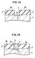
- FIGS 1A and 1B are sectional views showing processes according to the first embodiment of the present invention.
- a p-type silicon substrate 1 is subjected to an element separation and an arsenic (As) ion implantation, and activated to form an n+ diffusion layer 2 as shown in Fig. 1A.
- a silicon oxide film 3 is deposited on the substrate 1, and a contact hole 4 is formed by using a normal optical exposure method. Through the contact hole 4, an electrode is connected to the diffusion layer 2.
- the substrate 1 is properly processed chemically or physically to clean the silicon surface 2a and the silicon oxide film surface 3a, and then placed in a vacuum CVD furnace of a normal diffusion type.
- An argon gas of 0 to 2000cc/min and a hydrogen gas of 200 to 3000cc/min are introduced into the furnace, and the substrate 1 is heated to a predetermined temperature between 200°C and 600°C.
- the flow rate of the hydrogen (H2) gas is properly set according to deposition conditions and stabilized, and a dichlorosilane (SiH2Cl2) gas of 1 to 200cc/min is poured onto the substrate 1. At this time and within the above-mentioned temperature range, the dichlorosilane does not dissolve to deposit on the substrate 1.
- a WF6 gas of 0.1 to 100cc/min is added.
- a tungsten 5 selectively deposits on the silicon n+ diffusion layer surface 2a on the bottom of the contact hole 4 at a deposition speed of 100 to 15000 ⁇ /min as shown in Fig. 1B.
- the tungsten is not formed on the surface 3a of the silicon oxide film 3, i.e., the selectivity is perfect.
- the free energy change G in the reaction of tungsten and silane "III" is smaller than that in the reaction of tungsten and silicon. This means that the reaction of tungsten and silane may occur easier than that of tungsten and silicon, and that the "biting" phenomenon is remarkably suppressed by using the mixed gas of WF6 and SiH2 according to the present invention.
- dichlorosilane SiH
- a gas of silane, disilane, or the halides of the silane and disilane may be used instead of the dichlorosilane to provide the same effect.
- the case (i) with the H2 gas has a slower deposition speed than the case (ii) with the Ar gas, but the case (i) has a wider temperature range in which a predetermined deposition speed is obtainable as well as realizing a practical good film quality.
- selectivity depends on a flow rate Q1 of WF6 and a flow rate Q2 of SiH2Cl2, and that, as the flow rate Q1 is increased, the selectivity increases while a deposition speed of the tungsten film decreases. If the flow rate Q2 is increased, the deposition speed increases while the selectivity is deteriorated to form the tungsten film allover the substrate surface.
- a flow rate ratio with which a good selectivity can be provided is as follows: Q2/Q1 ⁇ 3.
- the selectivity tends to be deteriorated particular in a central region of the substrate when the ratio is Q2/Q1>2.
- the selectivity can be maintained sufficiently with a ratio of Q2/Q1 ⁇ 3 for a deposition temperature of 250°C ⁇ T ⁇ 350 p C, and with a ratio of Q2/Q1 ⁇ 1.5 for a deposition temperature of 350°C ⁇ T ⁇ 600°C.
- Deposition pressure is also an important factor influencing the selectively, and the good selectivity can be obtained with 0.01 to 5 torrs for the above-mentioned conditions. The lower the deposition pressure, the better the selectivity.
- FIGs 2A and 2B are sectional views showing processes for selectively forming a refractory metal film according to the second embodiment of the present invention.
- a silicon oxide film 7 with a thickness of 8000 ⁇ is formed on a p-type silicon substrate 6.
- a chemical spattering is used to form a titanium nitride (TiN) film 8 with a thickness of 1000A is formed on the film 7, and the titanium nitride film 8 is subjected to a patterning by a normal optical exposure method as shown in Fig. 2A.
- TiN titanium nitride
- the substrate is placed in a vacuum CVD furnace of a normal diffusion type.
- An argon gas of 0 to 2000cc/min and a hydrogen gas of 200 to 3000cc/min are poured onto the substrate which is heated to a predetermined temperature between 200°C to 600°C. Then, the flow rate of the hydrogen gas is properly adjusted according to the deposition conditions and stabilized.
- a dichlorosilane (SiH2Cl2) gas of 1 to 1000cc/min is poured onto the substrate. At this time, within the above-mentioned temperature range, SiH2Cl2 does not dissolve to deposit on the substrate.
- a WF6 gas of 0.1 to 100cc/min is added.
- a tungsten film 9 deposits with a deposition speed of 100 to 2000 ⁇ /min only on the titanium nitride film 8 as shown in Fig. 2B.
- a normal mixed gas of WF6 and H2 is used with the above-mentioned deposition conditions, the tungsten film does not deposit on the TiN film 8, or the tungsten film deposits allover the substrate surface but not over the TiN film 8.
- a reaction of WF6 and H2 in the prior art method occurs in a process where the adsorption and dissociation of hydrogen with respect to the substrate tends to govern the reaction.
- the adsorption and dissociation of hydrogen is easy to occur on the surface of a metal such as tungsten (W) while it is hard to occur on the surface of a material which has strong covalent bonding. Therefore, the deposition reaction of tungsten (W) is hard to occur on an oxide film or on a nitride film of metal or silicon.
- the adsorption and dissociation of SiH2Cl2 is larger than that of hydrogen. Further, the dissociation generates Si, H and Cl, and Si greatly contributes to the reduction of WF6 while H and Cl suppress the reaction speed to make the control of the reaction speed easier.
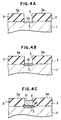
- Figures 3A to 3D are sectional views showing processes for forming a refractory metal film according to the third embodiment of the present invention.
- a p-type silicon substrate 10 is subjected to an element separation and an arsenic (As) ion implantation, and activated to form an n+ diffusion layer 11 thereon.
- a silicon dioxide film 12 is formed on the substrate, and a patterning is carried out by using a normal optical exposure method.
- the exposed silicon oxide film is etched by a reactive ion spattering method, etc., to form a contact hole 13 as shown in Fig. 3A.
- the substrate is then subjected to a proper dry processing and a wet processing.
- a titanium nitride (TiN) film 14 is formed on the contact hole 13 and on the silicon dioxide film 12 as shown in Fig. 3B.
- the optical exposure method and the reactive spattering method are used to leave the TiN film 14 on the bottom and side walls of the contact hole 13 as shown in Fig. 3C.
- the substrate is then placed in a vacuum CVD furnace to selectively deposit a tungsten 15 on the TiN as in the second embodiment to fill the contact hole 13 with the tungsten 15 to form a flat substrate surface as shown in Fig. 3D.
- Figures 4A to 4D are views showing processes for selectively forming a refractory metal film according to the fourth embodiment of the present invention.
- a p-type silicon substrate 1 is subjected to an element separation and an arsenic (As) ion implantation, and activated to form an n+ diffusion layer 2 thereon as shown in Fig. 4A.
- a silicon oxide film 3 is deposited on the substrate, and a contact hole 4 is formed by using a normal optical exposure method. Through the contact hole 4, an electrode is connected to the diffusion layer 2.
- On the surface of the substrate there are an exposed surface portion 2a of the n+ silicon diffusion layer 2 and an exposed surface portion 3a of the silicon oxide film 3.
- the substrate is chemically or physically processed to clean the silicon surface 2a and the silicon oxide film surface 3a, and placed in a vacuum CVD furnace of a normal diffusion type.
- a hydrogen gas is poured into the furnace at a flow rate of 200 to 3000cc/min, and the substrate is heated to a predetermined temperature between 250°C and 400°C.
- the flow rate of the hydrogen (H2) gas is properly set according to deposit conditions and stabilized.
- a WF6 gas of 0.5 to 50 cc/min is added at the temperature between 250°C and 400°C.
- a tungsten thin film 16 is selectively formed on the silicon surface 2a on the bottom of the contact hole 4 as shown in Fig. 4B.
- a hydrogen (H2) gas is poured onto the substrate according to the deposition conditions and stabilized.
- a dichlorosilane (SiH2Cl2) gas is then poured onto the substrate at a flow rate of 1 to 200cc/min.
- a WF6 gas is added at a flow rate of 1 to 100 cc/min. Due to this, as shown in Fig. 4°C, a tungsten 17 selectively deposits with a deposition speed of 100 to 15000 ⁇ /min on the tungsten thin film 16 in the contact hole 4. At this time, the tungsten does not deposit on the surface 3a of the silicon oxide film 3, i.e., the selectivity is perfect.
- the substrate is then heated to a predetermined temperature of 500°C, and a gas comprising N2 and H2 is added at a flow rate of 2cc/min to perform a heat treatment.
- the mixed gas of WF6 and H2 is used to form the tungsten thin film 16, and the mixed gas of WF6 and SiH2Cl2 to form the thick tungsten deposition layer 17 on the tungsten thin film 16. Due to the above, the "biting" phenomenon is suppressed and the adhesive force of tungsten with respect to the n+ diffusion layer 2 can be increased. Namely, when the mixed gas of WF6 and H2 is used, the amount of tungsten is sufficiently small to suppress the "biting" phenomenon. In addition, strong adhesive force is generated between the tungsten thin film 16 and the surface 2a of the n+ diffusion layer 2. When the mixed gas of WF6 and SiH2Cl2 is used, strong adhesive force is generated between the tungsten thin film 16 and the tungsten deposition layer 17.
- tungsten hexafluoride has been used as the halide of a refractory metal in the embodiments, it is possible to use as the refractory metal not only tungsten but also titanium, tantalum and molybdenum. In addition, the chloride of the refractory metal is also effective to use.
- halide of monosilace or disilane to be added will be not only SiH2Cl2 but also SiCl4, SiH2F2 SiF4, Si2H4Cl2, Si2H2Cl4, Si2Cl6, Si2H4F2, Si2H2F4 and Si2F6.
- the method according to the present invention can be used to form a refractory metal film of about 1000 ⁇ to be used as a barrier metal for the source, drain and gate regions of a MOS transistor.
- the refractory metal film can lower the resistance of a contact portion.
- the method for forming a refractory metal film according to the present invention utilizes a reduction reaction of the halide of refractory metal with respect to the halide of monosilane or disilane to form a refractory metal film while suppressing the reaction by adding a hydrogen gas.
- the refractory metal film can be formed with good quality at a high speed, or can selectively be deposited on the nitride of a metal.
Landscapes
- Internal Circuitry In Semiconductor Integrated Circuit Devices (AREA)
- Electrodes Of Semiconductors (AREA)
- Chemical Vapour Deposition (AREA)
Applications Claiming Priority (2)
| Application Number | Priority Date | Filing Date | Title |
|---|---|---|---|
| JP62171218A JP2592844B2 (ja) | 1987-07-10 | 1987-07-10 | 高融点金属膜の形成方法 |
| JP171218/87 | 1987-07-10 |
Publications (3)
| Publication Number | Publication Date |
|---|---|
| EP0298155A2 true EP0298155A2 (fr) | 1989-01-11 |
| EP0298155A3 EP0298155A3 (fr) | 1990-08-01 |
| EP0298155B1 EP0298155B1 (fr) | 1999-06-02 |
Family
ID=15919230
Family Applications (1)
| Application Number | Title | Priority Date | Filing Date |
|---|---|---|---|
| EP87117894A Expired - Lifetime EP0298155B1 (fr) | 1987-07-10 | 1987-12-03 | Procédé pour former une couche de métal réfractaire |
Country Status (4)
| Country | Link |
|---|---|
| EP (1) | EP0298155B1 (fr) |
| JP (1) | JP2592844B2 (fr) |
| KR (1) | KR910006971B1 (fr) |
| DE (1) | DE3752277T2 (fr) |
Cited By (3)
| Publication number | Priority date | Publication date | Assignee | Title |
|---|---|---|---|---|
| EP0363065A3 (fr) * | 1988-10-07 | 1990-07-25 | AT&T Corp. | Procédé de fabrication de dispositifs |
| DE4034868A1 (de) * | 1990-11-02 | 1992-05-07 | Itt Ind Gmbh Deutsche | Verfahren zur selektiven metallabscheidung bei der herstellung von halbleiterbauelementen |
| EP0437110A3 (fr) * | 1990-01-08 | 1994-01-05 | Lsi Logic Corp |
Families Citing this family (6)
| Publication number | Priority date | Publication date | Assignee | Title |
|---|---|---|---|---|
| JPH0656841B2 (ja) * | 1987-10-15 | 1994-07-27 | 日電アネルバ株式会社 | タングステンの選択成長方法 |
| JPH0623435B2 (ja) * | 1987-12-01 | 1994-03-30 | 日電アネルバ株式会社 | タングステン膜の減圧気相成長方法 |
| US5084417A (en) * | 1989-01-06 | 1992-01-28 | International Business Machines Corporation | Method for selective deposition of refractory metals on silicon substrates and device formed thereby |
| JP2803676B2 (ja) * | 1989-07-04 | 1998-09-24 | 富士通株式会社 | 半導体装置の製造方法 |
| JP4877687B2 (ja) * | 2000-07-28 | 2012-02-15 | 東京エレクトロン株式会社 | 成膜方法 |
| JP3696587B2 (ja) | 2002-10-11 | 2005-09-21 | 沖電気工業株式会社 | 半導体素子の製造方法 |
Family Cites Families (7)
| Publication number | Priority date | Publication date | Assignee | Title |
|---|---|---|---|---|
| JPS5776833A (en) * | 1980-09-04 | 1982-05-14 | Applied Materials Inc | Heat resistant metal depositing method and product thereof |
| DE3211752C2 (de) * | 1982-03-30 | 1985-09-26 | Siemens AG, 1000 Berlin und 8000 München | Verfahren zum selektiven Abscheiden von aus Siliziden hochschmelzender Metalle bestehenden Schichtstrukturen auf im wesentlichen aus Silizium bestehenden Substraten und deren Verwendung |
| DE3331759A1 (de) * | 1983-09-02 | 1985-03-21 | Siemens AG, 1000 Berlin und 8000 München | Integrierte halbleiterschaltung mit einer aus aluminium oder aus einer aluminium-legierung bestehenden mehrlagenverdrahtung und verfahren zu ihrer herstellung. |
| JPS60115245A (ja) * | 1983-11-28 | 1985-06-21 | Toshiba Corp | 半導体装置の製造方法 |
| JPS60145376A (ja) * | 1983-12-30 | 1985-07-31 | Fujitsu Ltd | タングステンシリサイド膜の成長方法 |
| DE3413064A1 (de) * | 1984-04-06 | 1985-10-31 | Siemens AG, 1000 Berlin und 8000 München | Verfahren zum herstellen von metallsilizidschichten durch abscheidung aus der gasphase bei vermindertem druck und deren verwendung |
| JPS61250172A (ja) * | 1985-04-25 | 1986-11-07 | Fujitsu Ltd | タングステンシリサイド膜の成長方法 |
-
1987
- 1987-07-10 JP JP62171218A patent/JP2592844B2/ja not_active Expired - Lifetime
- 1987-12-03 DE DE3752277T patent/DE3752277T2/de not_active Expired - Lifetime
- 1987-12-03 EP EP87117894A patent/EP0298155B1/fr not_active Expired - Lifetime
-
1988
- 1988-07-08 KR KR1019880008568A patent/KR910006971B1/ko not_active Expired
Cited By (3)
| Publication number | Priority date | Publication date | Assignee | Title |
|---|---|---|---|---|
| EP0363065A3 (fr) * | 1988-10-07 | 1990-07-25 | AT&T Corp. | Procédé de fabrication de dispositifs |
| EP0437110A3 (fr) * | 1990-01-08 | 1994-01-05 | Lsi Logic Corp | |
| DE4034868A1 (de) * | 1990-11-02 | 1992-05-07 | Itt Ind Gmbh Deutsche | Verfahren zur selektiven metallabscheidung bei der herstellung von halbleiterbauelementen |
Also Published As
| Publication number | Publication date |
|---|---|
| DE3752277D1 (de) | 1999-07-08 |
| DE3752277T2 (de) | 1999-11-04 |
| EP0298155A3 (fr) | 1990-08-01 |
| JP2592844B2 (ja) | 1997-03-19 |
| EP0298155B1 (fr) | 1999-06-02 |
| JPS6417866A (en) | 1989-01-20 |
| KR910006971B1 (ko) | 1991-09-14 |
| KR890003014A (ko) | 1989-04-12 |
Similar Documents
| Publication | Publication Date | Title |
|---|---|---|
| US5223455A (en) | Method of forming refractory metal film | |
| US6830820B2 (en) | Chemical vapor deposition of titanium | |
| US5420072A (en) | Method for forming a conductive interconnect in an integrated circuit | |
| US5442235A (en) | Semiconductor device having an improved metal interconnect structure | |
| US6077781A (en) | Single step process for blanket-selective CVD aluminum deposition | |
| US6287964B1 (en) | Method for forming a metallization layer of a semiconductor device | |
| US7402512B2 (en) | High aspect ratio contact structure with reduced silicon consumption | |
| US5963828A (en) | Method for tungsten nucleation from WF6 using titanium as a reducing agent | |
| EP0298155A2 (fr) | Procédé pour former une couche de métal réfractaire | |
| KR100530431B1 (ko) | 반도체장치형성프로세스 | |
| JP2005527098A (ja) | 高アスペクト比の半導体デバイス用のボロンドープ窒化チタン層 | |
| US5874360A (en) | Manufacture of semiconductor devices | |
| US5302846A (en) | Semiconductor device having improved vertical insulated gate type transistor | |
| US6245674B1 (en) | Method of forming a metal silicide comprising contact over a substrate | |
| US6433434B1 (en) | Apparatus having a titanium alloy layer | |
| US6291346B1 (en) | Titanium silicide layer formation method | |
| KR20030050652A (ko) | 텅스텐막의 형성 방법 | |
| US6239029B1 (en) | Sacrificial germanium layer for formation of a contact | |
| JP3246046B2 (ja) | 高融点金属膜の堆積方法 | |
| US20040224501A1 (en) | Manufacturing method for making tungsten-plug in an intergrated circuit device without volcano phenomena | |
| JPH1056017A (ja) | 半導体素子のビットライン及びその製造方法 | |
| JP3085745B2 (ja) | 半導体装置の製造方法 | |
| KR0150989B1 (ko) | 반도체소자 배선 형성방법 | |
| JPH01206623A (ja) | 半導体装置の製造方法 | |
| JPH08250585A (ja) | 半導体装置の製造方法 |
Legal Events
| Date | Code | Title | Description |
|---|---|---|---|
| PUAI | Public reference made under article 153(3) epc to a published international application that has entered the european phase |
Free format text: ORIGINAL CODE: 0009012 |
|
| AK | Designated contracting states |
Kind code of ref document: A2 Designated state(s): DE NL |
|
| PUAL | Search report despatched |
Free format text: ORIGINAL CODE: 0009013 |
|
| AK | Designated contracting states |
Kind code of ref document: A3 Designated state(s): DE NL |
|
| 17P | Request for examination filed |
Effective date: 19910131 |
|
| 17Q | First examination report despatched |
Effective date: 19910814 |
|
| APCB | Communication from the board of appeal sent |
Free format text: ORIGINAL CODE: EPIDOS OBAPE |
|
| APCB | Communication from the board of appeal sent |
Free format text: ORIGINAL CODE: EPIDOS OBAPE |
|
| APCB | Communication from the board of appeal sent |
Free format text: ORIGINAL CODE: EPIDOS OBAPE |
|
| APCB | Communication from the board of appeal sent |
Free format text: ORIGINAL CODE: EPIDOS OBAPE |
|
| APAB | Appeal dossier modified |
Free format text: ORIGINAL CODE: EPIDOS NOAPE |
|
| GRAG | Despatch of communication of intention to grant |
Free format text: ORIGINAL CODE: EPIDOS AGRA |
|
| GRAH | Despatch of communication of intention to grant a patent |
Free format text: ORIGINAL CODE: EPIDOS IGRA |
|
| GRAH | Despatch of communication of intention to grant a patent |
Free format text: ORIGINAL CODE: EPIDOS IGRA |
|
| GRAA | (expected) grant |
Free format text: ORIGINAL CODE: 0009210 |
|
| AK | Designated contracting states |
Kind code of ref document: B1 Designated state(s): DE NL |
|
| REF | Corresponds to: |
Ref document number: 3752277 Country of ref document: DE Date of ref document: 19990708 |
|
| PLBE | No opposition filed within time limit |
Free format text: ORIGINAL CODE: 0009261 |
|
| STAA | Information on the status of an ep patent application or granted ep patent |
Free format text: STATUS: NO OPPOSITION FILED WITHIN TIME LIMIT |
|
| 26N | No opposition filed | ||
| APAH | Appeal reference modified |
Free format text: ORIGINAL CODE: EPIDOSCREFNO |
|
| PGFP | Annual fee paid to national office [announced via postgrant information from national office to epo] |
Ref country code: DE Payment date: 20061130 Year of fee payment: 20 |
|
| PGFP | Annual fee paid to national office [announced via postgrant information from national office to epo] |
Ref country code: NL Payment date: 20061203 Year of fee payment: 20 |
|
| PG25 | Lapsed in a contracting state [announced via postgrant information from national office to epo] |
Ref country code: NL Free format text: LAPSE BECAUSE OF EXPIRATION OF PROTECTION Effective date: 20071203 |
|
| NLV7 | Nl: ceased due to reaching the maximum lifetime of a patent |
Effective date: 20071203 |