EP0300157A2 - Vertikale Transistor-/Kapazitätspeicherzellen-Struktur und Herstellungsverfahren dafür - Google Patents
Vertikale Transistor-/Kapazitätspeicherzellen-Struktur und Herstellungsverfahren dafür Download PDFInfo
- Publication number
- EP0300157A2 EP0300157A2 EP88108135A EP88108135A EP0300157A2 EP 0300157 A2 EP0300157 A2 EP 0300157A2 EP 88108135 A EP88108135 A EP 88108135A EP 88108135 A EP88108135 A EP 88108135A EP 0300157 A2 EP0300157 A2 EP 0300157A2
- Authority
- EP
- European Patent Office
- Prior art keywords
- polysilicon
- trench
- epitaxial
- layer
- epitaxial layer
- Prior art date
- Legal status (The legal status is an assumption and is not a legal conclusion. Google has not performed a legal analysis and makes no representation as to the accuracy of the status listed.)
- Granted
Links
Images




Classifications
-
- H—ELECTRICITY
- H10—SEMICONDUCTOR DEVICES; ELECTRIC SOLID-STATE DEVICES NOT OTHERWISE PROVIDED FOR
- H10B—ELECTRONIC MEMORY DEVICES
- H10B12/00—Dynamic random access memory [DRAM] devices
- H10B12/01—Manufacture or treatment
- H10B12/02—Manufacture or treatment for one transistor one-capacitor [1T-1C] memory cells
- H10B12/03—Making the capacitor or connections thereto
- H10B12/038—Making the capacitor or connections thereto the capacitor being in a trench in the substrate
- H10B12/0383—Making the capacitor or connections thereto the capacitor being in a trench in the substrate wherein the transistor is vertical
-
- H—ELECTRICITY
- H10—SEMICONDUCTOR DEVICES; ELECTRIC SOLID-STATE DEVICES NOT OTHERWISE PROVIDED FOR
- H10D—INORGANIC ELECTRIC SEMICONDUCTOR DEVICES
- H10D1/00—Resistors, capacitors or inductors
- H10D1/01—Manufacture or treatment
- H10D1/045—Manufacture or treatment of capacitors having potential barriers, e.g. varactors
- H10D1/047—Manufacture or treatment of capacitors having potential barriers, e.g. varactors of conductor-insulator-semiconductor capacitors, e.g. trench capacitors
-
- H—ELECTRICITY
- H10—SEMICONDUCTOR DEVICES; ELECTRIC SOLID-STATE DEVICES NOT OTHERWISE PROVIDED FOR
- H10D—INORGANIC ELECTRIC SEMICONDUCTOR DEVICES
- H10D1/00—Resistors, capacitors or inductors
- H10D1/60—Capacitors
- H10D1/62—Capacitors having potential barriers
- H10D1/66—Conductor-insulator-semiconductor capacitors, e.g. MOS capacitors
- H10D1/665—Trench conductor-insulator-semiconductor capacitors, e.g. trench MOS capacitors
Definitions
- the present invention relates to dynamic random access memory cell structures and fabrication methods therefor, and more particularly to a vertical trench transistor and trench capacitor structure and fabrication process therefor.
- Japanese Patent 59-19366 describes a vertical FET semiconductor memory device disposed between condensers for storing charge. Electrostatic capacity from the device substrate is utilized for storing the memory charge.
- Japanese Patent 56-100523 relates to a vertical one-transistor MOS memory cell having a cylindrical gate electrode, an insulating layer and source and drain layers.
- the source or drain layer can also be one electrode of a charge storage capacitor.
- the publication entitled DYNAMIC RAM CELL STRUCTURE, IBM Technical Disclosure Bulletin, Vol 27, No. 12, May 1985 at page 7051 relates generally to integrated circuit structures and more particularly to dynamic random-access memory (DRAM) cell construction having a stacked planar MOS access transistor over a buried pn junction storage capacitor.
- DRAM dynamic random-access memory
- An object of the present invention is to provide an improved high density one-transistor dynamic random-access-memory (DRAM) cell structure.
- DRAM dynamic random-access-memory
- Another object of the present invention is to provide an improved memory cell structure including a vertical transistor and trench capacitor.
- Another object of the present invention is to provide an improved DRAM cell structure which has a vertical transistor built on the surfaces of a U-groove between the surface of the silicon and a trench storage capacitor buried beneath the U-groove.
- Another object of the present invention is to provide an improved fabrication process for providing high density by decoupling the dimensions of the vertical access transistor from the size of trench storage capacitor.
- Another object of the present invention is to provide an improved fabrication process for providing an epitaxial layer on a silicon substrate and over predefined insulator-capped islands, which forms a self-aligned contact connection in the epitaxial layer.
- Still another object of the present invention is to provide an improved fabrication process for providing a connection between the vertical device made in the epitaxial layer and the device below the predefined insulator-capped islands and forming a self-aligned contact-connection in the epitaxial layer.
- a further object of the present invention is to provide a fabrication method for a DRAM device wherein the connection between the source region of the vertical access transistor and the storage electrode of the trench capacitor is formed by two selective epitaxial growth to provide a self-aligned contact.
- FIG. 1 shows a U-groove shallow trench access transistor 10 stacked on top of a U-groove deep substrate-plate trench (SPT) storage capacitor 22.
- SPT substrate-plate trench
- Arrangement of the vertical access transistor 10 and the trench storage capacitor 22 as shown in Fig. 1 are different from those of the conventional planar and trench DRAM cells described by H. Sunami in the publication "Cell structures for future DRAM's", IEDM Tech. Dig., pp. 694-697, 1985 and by W. F.
- the new cell is fabricated successfully by using a new self-alignment epitaxial growth method in combination with state-of-the-art CMOS technologies.
- Two epitaxial layers are grown with an intervening oxide etching step over a substrate wafer already provided with trench storage capacitors.
- the first and second epitaxial layers simultaneously grow vertically on the bare silicon surrounding the buried storage capacitor and laterally over the oxide.
- the trench transistor is fabricated in the epitaxial layers.
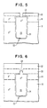
- Fig. 1 illustrates a cross-sectional view of a U-SPT cell fabricated using the method of the present invention illustrated in Figs. 3 through 10, with a top view shown in Fig. 2.
- the structure of the device of Fig. 1 includes a silicon substrate 16 which, for the purposes of explanation, is p+ type.
- a p-channel transfer device with gate 48, source 44, and drain 40 is made in an n-well region 36 within a p-type epitaxial layer 14.
- a trench capacitor is located in substrate 16 and filled with heavily doped p+ polysilicon 26.
- a composite film 24 of SiO2/Si3N4/SiO2 on the trench sidewalls is provided for the capacitor storage insulator.
- a p+ doped vertical connection 34 is formed to connect the source region of the transfer device and the storage electrode 26 of the trench capacitor.
- An interconnection diffusion line 40 used for the bitline is connected to the drain region of the transfer device.
- the memory cell can be made n-channel device without loss of generality by reversing the dopant polarity of polysilicon trench fill 26, forming a p-type "well" region in epitaxial layers 14, 30 and 32, and forming n-channel FET devices as transfer devices in the p-type well.
- the new U-SPT cell has solved several problems of prior art memory cells and has a better packing density and electrical behavior.
- the advantages are as follows:
- the layout of the new cell as shown in Fig. 2 results in high density because the cell is located at a cross-point between the wordline and bitline, and the cell transistor and capacitor are vertically oriented.
- the cell can have a large capacitor top surface area and a small transistor planar surface area because the minimum cell size of this new cell of Figs. 1 and 2 is determined by the opening of the deep trench capacitor, but not by the opening of the trench transistor.
- the processes to form the novel buried connection between the access transistor and storage capacitor, and to form the buried source junction of the access transistor have self-alignment feature.
- the access transistor is a bulk transistor and is different from other 3-D silicon-on-insulator (SOI) DRAM cells in that the U-SPT cell can have a high quality crystalline transistor with stable body bias. Furthermore, the storage node is inside the trench and the access device is fabricated in an n-well, which can achieve lower soft error rate, higher noise immunity and firmly grounded substrate plate.
- SOI silicon-on-insulator
Landscapes
- Engineering & Computer Science (AREA)
- Manufacturing & Machinery (AREA)
- Semiconductor Memories (AREA)
- Semiconductor Integrated Circuits (AREA)
Applications Claiming Priority (2)
| Application Number | Priority Date | Filing Date | Title |
|---|---|---|---|
| US75791 | 1987-07-20 | ||
| US07/075,791 US4816884A (en) | 1987-07-20 | 1987-07-20 | High density vertical trench transistor and capacitor memory cell structure and fabrication method therefor |
Publications (3)
| Publication Number | Publication Date |
|---|---|
| EP0300157A2 true EP0300157A2 (de) | 1989-01-25 |
| EP0300157A3 EP0300157A3 (en) | 1989-09-13 |
| EP0300157B1 EP0300157B1 (de) | 1993-05-05 |
Family
ID=22128011
Family Applications (1)
| Application Number | Title | Priority Date | Filing Date |
|---|---|---|---|
| EP88108135A Expired - Lifetime EP0300157B1 (de) | 1987-07-20 | 1988-05-20 | Vertikale Transistor-/Kapazitätspeicherzellen-Struktur und Herstellungsverfahren dafür |
Country Status (6)
| Country | Link |
|---|---|
| US (1) | US4816884A (de) |
| EP (1) | EP0300157B1 (de) |
| JP (1) | JPS6437865A (de) |
| BR (1) | BR8803623A (de) |
| CA (1) | CA1285333C (de) |
| DE (1) | DE3880750T2 (de) |
Cited By (20)
| Publication number | Priority date | Publication date | Assignee | Title |
|---|---|---|---|---|
| EP0399191A1 (de) * | 1989-05-22 | 1990-11-28 | International Business Machines Corporation | Verfahren zur Herstellung eines sichselbstjustierenden Transistors mit schwach dotiertem Drain und Source in einem Graben |
| US6281539B1 (en) * | 2000-03-31 | 2001-08-28 | International Business Machines Corporation | Structure and process for 6F2 DT cell having vertical MOSFET and large storage capacitance |
| US8861247B2 (en) | 2009-04-27 | 2014-10-14 | Micron Technology, Inc. | Techniques for providing a direct injection semiconductor memory device |
| US8947965B2 (en) | 2009-07-27 | 2015-02-03 | Micron Technology Inc. | Techniques for providing a direct injection semiconductor memory device |
| US8964479B2 (en) | 2010-03-04 | 2015-02-24 | Micron Technology, Inc. | Techniques for sensing a semiconductor memory device |
| US8982633B2 (en) | 2009-05-22 | 2015-03-17 | Micron Technology, Inc. | Techniques for providing a direct injection semiconductor memory device |
| US9019788B2 (en) | 2008-01-24 | 2015-04-28 | Micron Technology, Inc. | Techniques for accessing memory cells |
| US9019759B2 (en) | 2010-03-15 | 2015-04-28 | Micron Technology, Inc. | Techniques for providing a semiconductor memory device |
| US9064730B2 (en) | 2009-03-04 | 2015-06-23 | Micron Technology, Inc. | Techniques for forming a contact to a buried diffusion layer in a semiconductor memory device |
| US9093311B2 (en) | 2009-03-31 | 2015-07-28 | Micron Technology, Inc. | Techniques for providing a semiconductor memory device |
| US9142264B2 (en) | 2010-05-06 | 2015-09-22 | Micron Technology, Inc. | Techniques for refreshing a semiconductor memory device |
| US9240496B2 (en) | 2009-04-30 | 2016-01-19 | Micron Technology, Inc. | Semiconductor device with floating gate and electrically floating body |
| US9257155B2 (en) | 2007-05-30 | 2016-02-09 | Micron Technology, Inc. | Integrated circuit having voltage generation circuitry for memory cell array, and method of operating and/or controlling same |
| US9263133B2 (en) | 2011-05-17 | 2016-02-16 | Micron Technology, Inc. | Techniques for providing a semiconductor memory device |
| US9276000B2 (en) | 2007-03-29 | 2016-03-01 | Micron Technology, Inc. | Manufacturing process for zero-capacitor random access memory circuits |
| US9331083B2 (en) | 2009-07-10 | 2016-05-03 | Micron Technology, Inc. | Techniques for providing a semiconductor memory device |
| US9553186B2 (en) | 2008-09-25 | 2017-01-24 | Micron Technology, Inc. | Recessed gate silicon-on-insulator floating body device with self-aligned lateral isolation |
| US9812179B2 (en) | 2009-11-24 | 2017-11-07 | Ovonyx Memory Technology, Llc | Techniques for reducing disturbance in a semiconductor memory device |
| US10304837B2 (en) | 2007-11-29 | 2019-05-28 | Ovonyx Memory Technology, Llc | Integrated circuit having memory cell array including barriers, and method of manufacturing same |
| US10418091B2 (en) | 2005-09-07 | 2019-09-17 | Ovonyx Memory Technology, Llc | Memory cell and memory cell array having an electrically floating body transistor, and methods of operating same |
Families Citing this family (76)
| Publication number | Priority date | Publication date | Assignee | Title |
|---|---|---|---|---|
| US5017504A (en) * | 1986-12-01 | 1991-05-21 | Mitsubishi Denki Kabushiki Kaisha | Vertical type MOS transistor and method of formation thereof |
| JPS63237460A (ja) * | 1987-03-25 | 1988-10-03 | Mitsubishi Electric Corp | 半導体装置 |
| US5028980A (en) * | 1988-12-21 | 1991-07-02 | Texas Instruments Incorporated | Trench capacitor with expanded area |
| US5124766A (en) * | 1989-06-30 | 1992-06-23 | Texas Instruments Incorporated | Filament channel transistor interconnected with a conductor |
| JP2529781B2 (ja) * | 1990-04-03 | 1996-09-04 | エレクトロニクス アンド テレコミュニケーションズ リサーチ インスティテュート | 垂直トランジスタ―を有するスタック−トレンチ構造のdramセルおよびその製造方法 |
| JPH04212450A (ja) * | 1990-04-11 | 1992-08-04 | Mitsubishi Electric Corp | 半導体記憶装置およびその製造方法 |
| US5107459A (en) * | 1990-04-20 | 1992-04-21 | International Business Machines Corporation | Stacked bit-line architecture for high density cross-point memory cell array |
| US4988637A (en) * | 1990-06-29 | 1991-01-29 | International Business Machines Corp. | Method for fabricating a mesa transistor-trench capacitor memory cell structure |
| US5055898A (en) * | 1991-04-30 | 1991-10-08 | International Business Machines Corporation | DRAM memory cell having a horizontal SOI transfer device disposed over a buried storage node and fabrication methods therefor |
| TW313677B (de) * | 1991-08-14 | 1997-08-21 | Gold Star Electronics | |
| US5365097A (en) * | 1992-10-05 | 1994-11-15 | International Business Machines Corporation | Vertical epitaxial SOI transistor, memory cell and fabrication methods |
| US5363327A (en) * | 1993-01-19 | 1994-11-08 | International Business Machines Corporation | Buried-sidewall-strap two transistor one capacitor trench cell |
| EP0683921B1 (de) * | 1993-02-04 | 2004-06-16 | Cornell Research Foundation, Inc. | Mikrostrukturen und einzelmask, einkristall-herstellungsverfahren |
| US5641694A (en) * | 1994-12-22 | 1997-06-24 | International Business Machines Corporation | Method of fabricating vertical epitaxial SOI transistor |
| US6236079B1 (en) | 1997-12-02 | 2001-05-22 | Kabushiki Kaisha Toshiba | Dynamic semiconductor memory device having a trench capacitor |
| US6069390A (en) | 1998-01-15 | 2000-05-30 | International Business Machines Corporation | Semiconductor integrated circuits with mesas |
| US6177299B1 (en) | 1998-01-15 | 2001-01-23 | International Business Machines Corporation | Transistor having substantially isolated body and method of making the same |
| US6177699B1 (en) | 1998-03-19 | 2001-01-23 | Lsi Logic Corporation | DRAM cell having a verticle transistor and a capacitor formed on the sidewalls of a trench isolation |
| US6369418B1 (en) | 1998-03-19 | 2002-04-09 | Lsi Logic Corporation | Formation of a novel DRAM cell |
| US6037620A (en) * | 1998-06-08 | 2000-03-14 | International Business Machines Corporation | DRAM cell with transfer device extending along perimeter of trench storage capacitor |
| US5915183A (en) * | 1998-06-26 | 1999-06-22 | International Business Machines Corporation | Raised source/drain using recess etch of polysilicon |
| US6140175A (en) * | 1999-03-03 | 2000-10-31 | International Business Machines Corporation | Self-aligned deep trench DRAM array device |
| US6376873B1 (en) | 1999-04-07 | 2002-04-23 | International Business Machines Corporation | Vertical DRAM cell with robust gate-to-storage node isolation |
| DE10027913A1 (de) * | 2000-05-31 | 2001-12-13 | Infineon Technologies Ag | Speicherzelle mit einem Grabenkondensator |
| US6621112B2 (en) * | 2000-12-06 | 2003-09-16 | Infineon Technologies Ag | DRAM with vertical transistor and trench capacitor memory cells and methods of fabrication |
| US6774426B2 (en) * | 2000-12-19 | 2004-08-10 | Micron Technology, Inc. | Flash cell with trench source-line connection |
| US6537920B1 (en) * | 2001-03-16 | 2003-03-25 | Advanced Micro Devices, Inc. | Formation of vertical transistors using block copolymer lithography |
| TWI230392B (en) | 2001-06-18 | 2005-04-01 | Innovative Silicon Sa | Semiconductor device |
| US6620676B2 (en) | 2001-06-29 | 2003-09-16 | International Business Machines Corporation | Structure and methods for process integration in vertical DRAM cell fabrication |
| EP1357603A3 (de) | 2002-04-18 | 2004-01-14 | Innovative Silicon SA | Halbleiterbauelement |
| EP1355316B1 (de) | 2002-04-18 | 2007-02-21 | Innovative Silicon SA | Datenspeichergerät sowie Verfahren zum Auffrischen der auf einem solchen Gerät gespeicherten Daten |
| JP4212838B2 (ja) * | 2002-06-26 | 2009-01-21 | カルピス株式会社 | 抗アレルギー剤 |
| US6727540B2 (en) * | 2002-08-23 | 2004-04-27 | International Business Machines Corporation | Structure and method of fabricating embedded DRAM having a vertical device array and a bordered bitline contact |
| KR100854816B1 (ko) * | 2003-03-13 | 2008-08-27 | 기린 홀딩스 가부시키가이샤 | 항알레르기용 조성물 |
| US6909137B2 (en) * | 2003-04-07 | 2005-06-21 | International Business Machines Corporation | Method of creating deep trench capacitor using a P+ metal electrode |
| US7085153B2 (en) | 2003-05-13 | 2006-08-01 | Innovative Silicon S.A. | Semiconductor memory cell, array, architecture and device, and method of operating same |
| US20040228168A1 (en) | 2003-05-13 | 2004-11-18 | Richard Ferrant | Semiconductor memory device and method of operating same |
| US6912150B2 (en) | 2003-05-13 | 2005-06-28 | Lionel Portman | Reference current generator, and method of programming, adjusting and/or operating same |
| US7335934B2 (en) | 2003-07-22 | 2008-02-26 | Innovative Silicon S.A. | Integrated circuit device, and method of fabricating same |
| US7184298B2 (en) | 2003-09-24 | 2007-02-27 | Innovative Silicon S.A. | Low power programming technique for a floating body memory transistor, memory cell, and memory array |
| DE10345460B4 (de) * | 2003-09-30 | 2007-01-04 | Infineon Technologies Ag | Verfahren zur Herstellung eines Lochgraben-Speicherkondensators in einem Halbleitersubstrat |
| US7476939B2 (en) | 2004-11-04 | 2009-01-13 | Innovative Silicon Isi Sa | Memory cell having an electrically floating body transistor and programming technique therefor |
| US7251164B2 (en) | 2004-11-10 | 2007-07-31 | Innovative Silicon S.A. | Circuitry for and method of improving statistical distribution of integrated circuits |
| US7301838B2 (en) | 2004-12-13 | 2007-11-27 | Innovative Silicon S.A. | Sense amplifier circuitry and architecture to write data into and/or read from memory cells |
| US7301803B2 (en) | 2004-12-22 | 2007-11-27 | Innovative Silicon S.A. | Bipolar reading technique for a memory cell having an electrically floating body transistor |
| US7485910B2 (en) * | 2005-04-08 | 2009-02-03 | International Business Machines Corporation | Simplified vertical array device DRAM/eDRAM integration: method and structure |
| US7355916B2 (en) | 2005-09-19 | 2008-04-08 | Innovative Silicon S.A. | Method and circuitry to generate a reference current for reading a memory cell, and device implementing same |
| US7683430B2 (en) | 2005-12-19 | 2010-03-23 | Innovative Silicon Isi Sa | Electrically floating body memory cell and array, and method of operating or controlling same |
| US7542345B2 (en) | 2006-02-16 | 2009-06-02 | Innovative Silicon Isi Sa | Multi-bit memory cell having electrically floating body transistor, and method of programming and reading same |
| US7492632B2 (en) | 2006-04-07 | 2009-02-17 | Innovative Silicon Isi Sa | Memory array having a programmable word length, and method of operating same |
| US7606098B2 (en) | 2006-04-18 | 2009-10-20 | Innovative Silicon Isi Sa | Semiconductor memory array architecture with grouped memory cells, and method of controlling same |
| WO2007128738A1 (en) | 2006-05-02 | 2007-11-15 | Innovative Silicon Sa | Semiconductor memory cell and array using punch-through to program and read same |
| US8069377B2 (en) | 2006-06-26 | 2011-11-29 | Micron Technology, Inc. | Integrated circuit having memory array including ECC and column redundancy and method of operating the same |
| US7542340B2 (en) | 2006-07-11 | 2009-06-02 | Innovative Silicon Isi Sa | Integrated circuit including memory array having a segmented bit line architecture and method of controlling and/or operating same |
| WO2008090475A2 (en) | 2007-01-26 | 2008-07-31 | Innovative Silicon S.A. | Floating-body dram transistor comprising source/drain regions separated from the gated body region |
| US8085594B2 (en) | 2007-06-01 | 2011-12-27 | Micron Technology, Inc. | Reading technique for memory cell with electrically floating body transistor |
| US8194487B2 (en) | 2007-09-17 | 2012-06-05 | Micron Technology, Inc. | Refreshing data of memory cells with electrically floating body transistors |
| US8349662B2 (en) | 2007-12-11 | 2013-01-08 | Micron Technology, Inc. | Integrated circuit having memory cell array, and method of manufacturing same |
| US20090159947A1 (en) * | 2007-12-19 | 2009-06-25 | International Business Machines Corporation | SIMPLIFIED VERTICAL ARRAY DEVICE DRAM/eDRAM INTEGRATION |
| US8014195B2 (en) | 2008-02-06 | 2011-09-06 | Micron Technology, Inc. | Single transistor memory cell |
| US8189376B2 (en) | 2008-02-08 | 2012-05-29 | Micron Technology, Inc. | Integrated circuit having memory cells including gate material having high work function, and method of manufacturing same |
| US7957206B2 (en) | 2008-04-04 | 2011-06-07 | Micron Technology, Inc. | Read circuitry for an integrated circuit having memory cells and/or a memory cell array, and method of operating same |
| US7933140B2 (en) | 2008-10-02 | 2011-04-26 | Micron Technology, Inc. | Techniques for reducing a voltage swing |
| US7924630B2 (en) | 2008-10-15 | 2011-04-12 | Micron Technology, Inc. | Techniques for simultaneously driving a plurality of source lines |
| US8223574B2 (en) | 2008-11-05 | 2012-07-17 | Micron Technology, Inc. | Techniques for block refreshing a semiconductor memory device |
| US8213226B2 (en) | 2008-12-05 | 2012-07-03 | Micron Technology, Inc. | Vertical transistor memory cell and array |
| US8319294B2 (en) | 2009-02-18 | 2012-11-27 | Micron Technology, Inc. | Techniques for providing a source line plane |
| US8199595B2 (en) | 2009-09-04 | 2012-06-12 | Micron Technology, Inc. | Techniques for sensing a semiconductor memory device |
| US8310893B2 (en) | 2009-12-16 | 2012-11-13 | Micron Technology, Inc. | Techniques for reducing impact of array disturbs in a semiconductor memory device |
| US8416636B2 (en) | 2010-02-12 | 2013-04-09 | Micron Technology, Inc. | Techniques for controlling a semiconductor memory device |
| US8411513B2 (en) | 2010-03-04 | 2013-04-02 | Micron Technology, Inc. | Techniques for providing a semiconductor memory device having hierarchical bit lines |
| US8369177B2 (en) | 2010-03-05 | 2013-02-05 | Micron Technology, Inc. | Techniques for reading from and/or writing to a semiconductor memory device |
| US8652925B2 (en) | 2010-07-19 | 2014-02-18 | International Business Machines Corporation | Method of fabricating isolated capacitors and structure thereof |
| US9559216B2 (en) | 2011-06-06 | 2017-01-31 | Micron Technology, Inc. | Semiconductor memory device and method for biasing same |
| CN110557969B (zh) * | 2018-04-03 | 2023-05-16 | 深圳市汇顶科技股份有限公司 | 阻变式存储器的制造方法和阻变式存储器 |
| US12002758B2 (en) | 2021-11-04 | 2024-06-04 | International Business Machines Corporation | Backside metal-insulator-metal (MIM) capacitors extending through backside interlayer dielectric (BILD) layer or semiconductor layer and partly through dielectric layer |
Family Cites Families (8)
| Publication number | Priority date | Publication date | Assignee | Title |
|---|---|---|---|---|
| JPS583269A (ja) * | 1981-06-30 | 1983-01-10 | Fujitsu Ltd | 縦型mosダイナミツクメモリ−セル |
| JPS5919366A (ja) * | 1982-07-23 | 1984-01-31 | Hitachi Ltd | 半導体記憶装置 |
| JPS5982761A (ja) * | 1982-11-04 | 1984-05-12 | Hitachi Ltd | 半導体メモリ |
| US4651184A (en) * | 1984-08-31 | 1987-03-17 | Texas Instruments Incorporated | Dram cell and array |
| JPS61179571A (ja) * | 1984-09-27 | 1986-08-12 | テキサス インスツルメンツ インコ−ポレイテツド | メモリセルおよびそのアレイ |
| DE3585136D1 (de) * | 1984-10-31 | 1992-02-20 | Texas Instruments Inc | Dram-zelle und verfahren. |
| CN1004734B (zh) * | 1984-12-07 | 1989-07-05 | 得克萨斯仪器公司 | 动态随机存取存贮器单元(dram)和生产方法 |
| US4649625A (en) * | 1985-10-21 | 1987-03-17 | International Business Machines Corporation | Dynamic memory device having a single-crystal transistor on a trench capacitor structure and a fabrication method therefor |
-
1987
- 1987-07-20 US US07/075,791 patent/US4816884A/en not_active Expired - Fee Related
-
1988
- 1988-05-20 JP JP63122245A patent/JPS6437865A/ja active Pending
- 1988-05-20 EP EP88108135A patent/EP0300157B1/de not_active Expired - Lifetime
- 1988-05-20 DE DE88108135T patent/DE3880750T2/de not_active Expired - Fee Related
- 1988-06-24 CA CA000570365A patent/CA1285333C/en not_active Expired - Lifetime
- 1988-07-19 BR BR8803623A patent/BR8803623A/pt not_active Application Discontinuation
Cited By (26)
| Publication number | Priority date | Publication date | Assignee | Title |
|---|---|---|---|---|
| EP0399191A1 (de) * | 1989-05-22 | 1990-11-28 | International Business Machines Corporation | Verfahren zur Herstellung eines sichselbstjustierenden Transistors mit schwach dotiertem Drain und Source in einem Graben |
| US6281539B1 (en) * | 2000-03-31 | 2001-08-28 | International Business Machines Corporation | Structure and process for 6F2 DT cell having vertical MOSFET and large storage capacitance |
| US11031069B2 (en) | 2005-09-07 | 2021-06-08 | Ovonyx Memory Technology, Llc | Memory cell and memory cell array having an electrically floating body transistor, and methods of operating same |
| US10418091B2 (en) | 2005-09-07 | 2019-09-17 | Ovonyx Memory Technology, Llc | Memory cell and memory cell array having an electrically floating body transistor, and methods of operating same |
| US9276000B2 (en) | 2007-03-29 | 2016-03-01 | Micron Technology, Inc. | Manufacturing process for zero-capacitor random access memory circuits |
| US9257155B2 (en) | 2007-05-30 | 2016-02-09 | Micron Technology, Inc. | Integrated circuit having voltage generation circuitry for memory cell array, and method of operating and/or controlling same |
| US11081486B2 (en) | 2007-11-29 | 2021-08-03 | Ovonyx Memory Technology, Llc | Integrated circuit having memory cell array including barriers, and method of manufacturing same |
| US10304837B2 (en) | 2007-11-29 | 2019-05-28 | Ovonyx Memory Technology, Llc | Integrated circuit having memory cell array including barriers, and method of manufacturing same |
| US9019788B2 (en) | 2008-01-24 | 2015-04-28 | Micron Technology, Inc. | Techniques for accessing memory cells |
| US9553186B2 (en) | 2008-09-25 | 2017-01-24 | Micron Technology, Inc. | Recessed gate silicon-on-insulator floating body device with self-aligned lateral isolation |
| US9064730B2 (en) | 2009-03-04 | 2015-06-23 | Micron Technology, Inc. | Techniques for forming a contact to a buried diffusion layer in a semiconductor memory device |
| US9093311B2 (en) | 2009-03-31 | 2015-07-28 | Micron Technology, Inc. | Techniques for providing a semiconductor memory device |
| US8861247B2 (en) | 2009-04-27 | 2014-10-14 | Micron Technology, Inc. | Techniques for providing a direct injection semiconductor memory device |
| US9425190B2 (en) | 2009-04-27 | 2016-08-23 | Micron Technology, Inc. | Techniques for providing a direct injection semiconductor memory device |
| US9240496B2 (en) | 2009-04-30 | 2016-01-19 | Micron Technology, Inc. | Semiconductor device with floating gate and electrically floating body |
| US8982633B2 (en) | 2009-05-22 | 2015-03-17 | Micron Technology, Inc. | Techniques for providing a direct injection semiconductor memory device |
| US9331083B2 (en) | 2009-07-10 | 2016-05-03 | Micron Technology, Inc. | Techniques for providing a semiconductor memory device |
| US9679612B2 (en) | 2009-07-27 | 2017-06-13 | Micron Technology, Inc. | Techniques for providing a direct injection semiconductor memory device |
| US8964461B2 (en) | 2009-07-27 | 2015-02-24 | Micron Technology, Inc. | Techniques for providing a direct injection semiconductor memory device |
| US8947965B2 (en) | 2009-07-27 | 2015-02-03 | Micron Technology Inc. | Techniques for providing a direct injection semiconductor memory device |
| US9812179B2 (en) | 2009-11-24 | 2017-11-07 | Ovonyx Memory Technology, Llc | Techniques for reducing disturbance in a semiconductor memory device |
| US8964479B2 (en) | 2010-03-04 | 2015-02-24 | Micron Technology, Inc. | Techniques for sensing a semiconductor memory device |
| US9524971B2 (en) | 2010-03-15 | 2016-12-20 | Micron Technology, Inc. | Techniques for providing a semiconductor memory device |
| US9019759B2 (en) | 2010-03-15 | 2015-04-28 | Micron Technology, Inc. | Techniques for providing a semiconductor memory device |
| US9142264B2 (en) | 2010-05-06 | 2015-09-22 | Micron Technology, Inc. | Techniques for refreshing a semiconductor memory device |
| US9263133B2 (en) | 2011-05-17 | 2016-02-16 | Micron Technology, Inc. | Techniques for providing a semiconductor memory device |
Also Published As
| Publication number | Publication date |
|---|---|
| BR8803623A (pt) | 1989-02-08 |
| US4816884A (en) | 1989-03-28 |
| DE3880750T2 (de) | 1993-10-28 |
| DE3880750D1 (de) | 1993-06-09 |
| JPS6437865A (en) | 1989-02-08 |
| EP0300157A3 (en) | 1989-09-13 |
| CA1285333C (en) | 1991-06-25 |
| EP0300157B1 (de) | 1993-05-05 |
Similar Documents
| Publication | Publication Date | Title |
|---|---|---|
| EP0300157B1 (de) | Vertikale Transistor-/Kapazitätspeicherzellen-Struktur und Herstellungsverfahren dafür | |
| EP0302204B1 (de) | Vertikal-Trench-Transistor-/Kapazitätsspeicherzellen-Struktur und Herstellungsverfahren dafür | |
| US5670388A (en) | Method of making contacted body silicon-on-insulator field effect transistor | |
| EP0220410B1 (de) | Dynamische Speichervorrichtung mit wahlfreiem Zugriff mit einem monokristallinen Transistor auf einer rillenartigen Kondensatorstruktur und Herstellungsverfahren dafür | |
| JP3466938B2 (ja) | 半導体メモリ装置及びその製造方法 | |
| EP0262294B1 (de) | Herstellungsverfahren zur Ausbildung eines selbstausrichtenden Kontaktfensters und einer Verbindung in einer epitaktischen Schicht und Bauelementstrukturen, die dieses Verfahren verwenden | |
| US5981332A (en) | Reduced parasitic leakage in semiconductor devices | |
| US4830978A (en) | Dram cell and method | |
| US5055898A (en) | DRAM memory cell having a horizontal SOI transfer device disposed over a buried storage node and fabrication methods therefor | |
| US6150210A (en) | Memory cell that includes a vertical transistor and a trench capacitor | |
| US6946700B2 (en) | Trench DRAM cell with vertical device and buried word lines | |
| KR100232393B1 (ko) | 반도체 기억장치 및 그의 제조방법 | |
| KR970004952B1 (ko) | 동적 랜덤 액세스 메모리 디바이스 및 그의 제조방법 | |
| US5064777A (en) | Fabrication method for a double trench memory cell device | |
| US6204140B1 (en) | Dynamic random access memory | |
| US6309924B1 (en) | Method of forming self-limiting polysilicon LOCOS for DRAM cell | |
| US5034787A (en) | Structure and fabrication method for a double trench memory cell device | |
| JP2002222873A (ja) | 改良たて型mosfet | |
| US4916524A (en) | Dram cell and method | |
| EP0203960B1 (de) | In einem graben hergestellter hochleistungskondensator für dram-zellen | |
| JP2819520B2 (ja) | Dramセル | |
| JPH07112047B2 (ja) | 半導体記憶装置及びその製造方法 | |
| KR920001397B1 (ko) | 트렌치 에피택셜 트랜지스터 셀의 구조 및 이의 제조방법 | |
| HK1009207A (en) | Memory cell that includes a vertical transistor and a trench capacitor |
Legal Events
| Date | Code | Title | Description |
|---|---|---|---|
| PUAI | Public reference made under article 153(3) epc to a published international application that has entered the european phase |
Free format text: ORIGINAL CODE: 0009012 |
|
| AK | Designated contracting states |
Kind code of ref document: A2 Designated state(s): CH DE ES FR GB IT LI NL SE |
|
| PUAL | Search report despatched |
Free format text: ORIGINAL CODE: 0009013 |
|
| 17P | Request for examination filed |
Effective date: 19890524 |
|
| AK | Designated contracting states |
Kind code of ref document: A3 Designated state(s): CH DE ES FR GB IT LI NL SE |
|
| 17Q | First examination report despatched |
Effective date: 19920626 |
|
| GRAA | (expected) grant |
Free format text: ORIGINAL CODE: 0009210 |
|
| PGFP | Annual fee paid to national office [announced via postgrant information from national office to epo] |
Ref country code: FR Payment date: 19930427 Year of fee payment: 6 |
|
| AK | Designated contracting states |
Kind code of ref document: B1 Designated state(s): CH DE ES FR GB IT LI NL SE |
|
| PG25 | Lapsed in a contracting state [announced via postgrant information from national office to epo] |
Ref country code: NL Effective date: 19930505 Ref country code: ES Free format text: THE PATENT HAS BEEN ANNULLED BY A DECISION OF A NATIONAL AUTHORITY Effective date: 19930505 |
|
| PGFP | Annual fee paid to national office [announced via postgrant information from national office to epo] |
Ref country code: GB Payment date: 19930505 Year of fee payment: 6 |
|
| PG25 | Lapsed in a contracting state [announced via postgrant information from national office to epo] |
Ref country code: LI Effective date: 19930531 Ref country code: CH Effective date: 19930531 |
|
| ET | Fr: translation filed | ||
| ITF | It: translation for a ep patent filed | ||
| REF | Corresponds to: |
Ref document number: 3880750 Country of ref document: DE Date of ref document: 19930609 |
|
| PGFP | Annual fee paid to national office [announced via postgrant information from national office to epo] |
Ref country code: SE Payment date: 19930702 Year of fee payment: 6 |
|
| NLV1 | Nl: lapsed or annulled due to failure to fulfill the requirements of art. 29p and 29m of the patents act | ||
| REG | Reference to a national code |
Ref country code: CH Ref legal event code: PL |
|
| PG25 | Lapsed in a contracting state [announced via postgrant information from national office to epo] |
Ref country code: DE Effective date: 19940201 |
|
| PLBE | No opposition filed within time limit |
Free format text: ORIGINAL CODE: 0009261 |
|
| STAA | Information on the status of an ep patent application or granted ep patent |
Free format text: STATUS: NO OPPOSITION FILED WITHIN TIME LIMIT |
|
| 26N | No opposition filed | ||
| PG25 | Lapsed in a contracting state [announced via postgrant information from national office to epo] |
Ref country code: GB Effective date: 19940520 |
|
| PG25 | Lapsed in a contracting state [announced via postgrant information from national office to epo] |
Ref country code: SE Effective date: 19940521 |
|
| GBPC | Gb: european patent ceased through non-payment of renewal fee |
Effective date: 19940520 |
|
| EUG | Se: european patent has lapsed |
Ref document number: 88108135.0 Effective date: 19941210 |
|
| PG25 | Lapsed in a contracting state [announced via postgrant information from national office to epo] |
Ref country code: FR Effective date: 19950131 |
|
| EUG | Se: european patent has lapsed |
Ref document number: 88108135.0 |
|
| REG | Reference to a national code |
Ref country code: FR Ref legal event code: ST |
|
| PG25 | Lapsed in a contracting state [announced via postgrant information from national office to epo] |
Ref country code: IT Free format text: LAPSE BECAUSE OF NON-PAYMENT OF DUE FEES;WARNING: LAPSES OF ITALIAN PATENTS WITH EFFECTIVE DATE BEFORE 2007 MAY HAVE OCCURRED AT ANY TIME BEFORE 2007. THE CORRECT EFFECTIVE DATE MAY BE DIFFERENT FROM THE ONE RECORDED. Effective date: 20050520 |