EP0300406B1 - Mécanisme de protection d'écriture pour mémoire non volatile - Google Patents
Mécanisme de protection d'écriture pour mémoire non volatile Download PDFInfo
- Publication number
- EP0300406B1 EP0300406B1 EP88111522A EP88111522A EP0300406B1 EP 0300406 B1 EP0300406 B1 EP 0300406B1 EP 88111522 A EP88111522 A EP 88111522A EP 88111522 A EP88111522 A EP 88111522A EP 0300406 B1 EP0300406 B1 EP 0300406B1
- Authority
- EP
- European Patent Office
- Prior art keywords
- write protect
- prom
- register
- write
- external event
- Prior art date
- Legal status (The legal status is an assumption and is not a legal conclusion. Google has not performed a legal analysis and makes no representation as to the accuracy of the status listed.)
- Expired - Lifetime
Links
Images

Classifications
-
- G—PHYSICS
- G06—COMPUTING OR CALCULATING; COUNTING
- G06F—ELECTRIC DIGITAL DATA PROCESSING
- G06F21/00—Security arrangements for protecting computers, components thereof, programs or data against unauthorised activity
- G06F21/70—Protecting specific internal or peripheral components, in which the protection of a component leads to protection of the entire computer
- G06F21/78—Protecting specific internal or peripheral components, in which the protection of a component leads to protection of the entire computer to assure secure storage of data
- G06F21/79—Protecting specific internal or peripheral components, in which the protection of a component leads to protection of the entire computer to assure secure storage of data in semiconductor storage media, e.g. directly-addressable memories
-
- G—PHYSICS
- G06—COMPUTING OR CALCULATING; COUNTING
- G06F—ELECTRIC DIGITAL DATA PROCESSING
- G06F12/00—Accessing, addressing or allocating within memory systems or architectures
- G06F12/14—Protection against unauthorised use of memory or access to memory
- G06F12/1458—Protection against unauthorised use of memory or access to memory by checking the subject access rights
- G06F12/1466—Key-lock mechanism
-
- G—PHYSICS
- G11—INFORMATION STORAGE
- G11C—STATIC STORES
- G11C16/00—Erasable programmable read-only memories
- G11C16/02—Erasable programmable read-only memories electrically programmable
- G11C16/06—Auxiliary circuits, e.g. for writing into memory
-
- G—PHYSICS
- G11—INFORMATION STORAGE
- G11C—STATIC STORES
- G11C16/00—Erasable programmable read-only memories
- G11C16/02—Erasable programmable read-only memories electrically programmable
- G11C16/06—Auxiliary circuits, e.g. for writing into memory
- G11C16/10—Programming or data input circuits
- G11C16/102—External programming circuits, e.g. EPROM programmers; In-circuit programming or reprogramming; EPROM emulators
-
- G—PHYSICS
- G11—INFORMATION STORAGE
- G11C—STATIC STORES
- G11C16/00—Erasable programmable read-only memories
- G11C16/02—Erasable programmable read-only memories electrically programmable
- G11C16/06—Auxiliary circuits, e.g. for writing into memory
- G11C16/22—Safety or protection circuits preventing unauthorised or accidental access to memory cells
Definitions
- the present invention relates, in general, to a write protect mechanism for a non-volatile memory. More particularly, the invention relates to a mechanism for protecting programmable read-only memory (PROM) which comprises a portion of a computer system from inadvertant writes.
- PROM programmable read-only memory
- PROM-type memories either EPROM (erasable, programmable read-only memory) or EEPROM (electrically-erasable, programmable read-only memory), in both single-chip and board-level computers and controllers is rapidly increasing.
- a PROM may store, for instance, an odometer reading in the case of an automotive controller or an account balance in the case of a "smart" banking card. Such parameters must be subject to occasional alteration, but must also remain valid during periods of power-down and be protected from inadvertant alteration.
- the former write protection approach operates on the principle that if the programming process is made more complex, it is more likely that any time the process is properly executed it is the result of an intentional attempt to program the PROM. However, since the sequence of instructions for programming the PROM must reside somewhere in program memory, and since there are times during power transitions when the system may be "wildly" executing instructions, there is some probability that the programming sequence will be hit and the contents of the PROM inadvertantly altered.
- U.S. Patent 4,638,457 discloses a method of increasing the reliability of data stored in a PROM, but protects only against incomplete writes, not against inadvertant, but complete, writes.
- U.S. Patent 4,580,246, commonly assigned with the present Invention discloses a method of write protection for control registers. Writes to the control registers are allowed only once, and only within a short, predetermined time after the system is reset. After that period, no writes are allowed until the system is reset again. Obviously, this is reliable protection for certain types of control and configuration information, but cannot be used for PROM containing relatively large blocks of data, such as engine control parameters in an automotive controller, which would require more than the allowed period of time to re-program.
- Still a further object of the present invention is to provide an apparatus and method for providing independent write protection for a plurality of independently write protectable blocks of PROM.
- a write protect apparatus for use in a system, the system comprising a PROM, a write protect register, clock means for providing a clock signal and write protect means for allowing writes to the PROM if and only if the write protect register contains predetermined data
- the write protect apparatus comprising: timer means responsive to the clock signal and to an external event to generate a time-out signal a predetermined number of cycles of the clock signal after the occurence of the external event; and register protect means responsive to the external event and to the time-out signal for allowing the writing of the predetermined data into the write protect register only in the period between the occurence of the external event and the generation of the time-out signal.
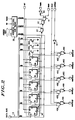
- FIG. 1 a single-chip microcomputer 10 is illustrated in block diagram form. While the present invention is disclosed in the context of this preferred embodiment, the principles of the present invention are applicable to board-level computer systems, memory systems and other embodiments.
- a time-out signal TIM80 provides the basis for the timing aspect of the block protect mechanism being described.
- TIM80 goes to a logic low state whenever a system reset is initiated and remains low for 64 E-clock cycles after microcomputer 10 comes out of reset and begins executing instructions, then goes high.
- the generation and use of a signal such as TIM80 are described in greater detail in U.S. Patent 4,580,246.
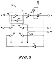
- a drain terminal of an N-channel transistor 65 is coupled to terminal 54 of latch 51.
- a source terminal of transistor 65 is coupled to a drain terminal of an N- channel transistor 66.
- a source terminal of transistor 66 is coupled to ground.
- a gate terminal of transistor 65 is coupled to the R input of latch circuit 50.
- a gate terminal of transistor 66 is coupled to an output of an inverter 67.
- An input of inverter 67 is coupled to bidirectional terminal D.
Landscapes
- Engineering & Computer Science (AREA)
- Computer Security & Cryptography (AREA)
- Theoretical Computer Science (AREA)
- Physics & Mathematics (AREA)
- General Engineering & Computer Science (AREA)
- General Physics & Mathematics (AREA)
- Computer Hardware Design (AREA)
- Software Systems (AREA)
- Storage Device Security (AREA)
Claims (9)
- Appareil de protection d'écriture destiné à être utilisé dans un système (10), le système comprenant une mémoire morte programmable PROM (22), un registre de protection d'écriture (30), un moyen d'horloge (26) pour produire un signal d'horloge et un moyen de protection d'écriture (23) pour permettre des écritures dans la PROM (22) si et seulement si le registre de protection d'écriture (30) contient des données prédéterminées, l'appareil de protection d'écriture comprenant :
un moyen de minuterie (26) sensible au signal d'horloge et à un événement externe pour générer un signal de dépassement de temps imparti (TIM80) un nombre prédéterminé de cycles du signal d'horloge après la survenue de l'événement externe ; et
un moyen de protection de registre (40, 41, 42, 43) sensible à l'événement externe et au signal de dépassement de temps imparti (TIM80) pour permettre l'écriture des données prédéterminées dans le registre de protection d'écriture (30) seulement pendant la période se situant entre la survenue de l'événement externe et de la génération du signal de dépassement de temps imparti (TIM 80). - Appareil selon la revendication 1, dans lequel :
le registre de protection d'écriture (30) est sensible à l'événement externe pour stocker des données autres que les données prédéterminées. - Appareil selon la revendication 2, dans lequel :
l'événement externe est une remise à l'état initial. - Appareil selon la revendication 1, dans lequel :
le registre de protection d'écriture (30) comprend en outre une pluralité d'emplacements de stockage de bits (31A-31E) ;
la PROM (22) comprend des parties pouvant être protégées séparément vis-à-vis d'une écriture en un nombre égal au nombre d'emplacements de stockage de bits dans le registre de protection d'écriture (30) ; et
le moyen de protection d'écriture (23) comprend en outre un moyen (45A-45E et 46A-46E) pour permettre des écritures dans chacune des parties pouvant être protégées séparément vis-à-vis d'une écriture seulement si l'un prédéterminé desdits emplacements de stockage de bits (31A-31E) est dans un premier état prédéterminé. - Appareil selon la revendication 1, dans lequel le moyen de protection d'écriture (23) comprend en outre :
un moyen (45A-45E et 46A-46E) pour invalider de façon sélective un décodeur d'adresse. - Appareil selon la revendication 1, comprenant en outre :
un moyen de configuration (EELAT) pour configurer la PROM (22) pour la programmation ou pour la lecture seulement, le moyen de protection d'écriture (23) étant sensible au moyen de configuration pour permettre un accès à la PROM indépendamment de l'information stockée dans ledit moyen de registre de protection (30) si la PROM est configurée pour la lecture seulement. - Système de traitement de données (10) comprenant :
un moyen d'unité centrale de traitement CPU (11) pour exécuter des instructions ; et
un appareil de protection d'écriture selon l'une quelconque des revendications précédentes. - Système de traitement de données selon la revendication 7, dans lequel :
le moyen de CPU (11) peut stocker une information autre que les données prédéterminées dans le registre de protection d'écriture (30) indépendamment de la génération du signal de dépassement de temps imparti (TIM80). - Procédé de protection d'une PROM (22), dans un système comprenant la PROM (22), un registre de protection d'écriture (30), un moyen d'horloge (26) pour produire un signal d'horloge et un moyen de protection d'écriture (23) pour permettre des écritures dans la PROM si et seulement si le registre de protection d'écriture (30) contient des données prédéterminées, le procédé protégeant la PROM (22) vis-à-vis d'écritures effectuées par inadvertance, et comprenant les étapes de :
réponse à un événement externe et au signal d'horloge au moyen de la génération d'un signal de dépassement de temps imparti (TIM80) un nombre prédéterminé de cycles du signal d'horloge après la survenue de l'événement externe ; et
autorisation de l'écriture des données prédéterminées dans le registre de protection d'écriture (30) seulement pendant la période se situant entre la survenue de l'événement externe et de la génération du signal de dépassement de temps imparti (TIM80).
Applications Claiming Priority (2)
| Application Number | Priority Date | Filing Date | Title |
|---|---|---|---|
| US07/076,509 US4796235A (en) | 1987-07-22 | 1987-07-22 | Write protect mechanism for non-volatile memory |
| US76509 | 1993-06-14 |
Publications (3)
| Publication Number | Publication Date |
|---|---|
| EP0300406A2 EP0300406A2 (fr) | 1989-01-25 |
| EP0300406A3 EP0300406A3 (fr) | 1992-01-15 |
| EP0300406B1 true EP0300406B1 (fr) | 1994-05-04 |
Family
ID=22132466
Family Applications (1)
| Application Number | Title | Priority Date | Filing Date |
|---|---|---|---|
| EP88111522A Expired - Lifetime EP0300406B1 (fr) | 1987-07-22 | 1988-07-18 | Mécanisme de protection d'écriture pour mémoire non volatile |
Country Status (4)
| Country | Link |
|---|---|
| US (1) | US4796235A (fr) |
| EP (1) | EP0300406B1 (fr) |
| JP (1) | JP2597153B2 (fr) |
| DE (1) | DE3889390T2 (fr) |
Families Citing this family (40)
| Publication number | Priority date | Publication date | Assignee | Title |
|---|---|---|---|---|
| JPS6382534A (ja) * | 1986-09-26 | 1988-04-13 | Matsushita Electric Ind Co Ltd | メモリ保護装置 |
| US4918690A (en) * | 1987-11-10 | 1990-04-17 | Echelon Systems Corp. | Network and intelligent cell for providing sensing, bidirectional communications and control |
| JP2712128B2 (ja) * | 1988-10-11 | 1998-02-10 | 株式会社日立製作所 | 半導体記憶装置 |
| US5083293A (en) * | 1989-01-12 | 1992-01-21 | General Instrument Corporation | Prevention of alteration of data stored in secure integrated circuit chip memory |
| US5278786A (en) * | 1989-04-11 | 1994-01-11 | Mitsubishi Denki Kabushiki Kaisha | Non-volatile semiconductor memory device having an area responsive to writing allowance signal |
| US5381366A (en) * | 1989-04-11 | 1995-01-10 | Mitsubishi Denki Kabushiki Kaisha | Non-volatile semiconductor memory device with timer controlled re-write inhibit means |
| US7447069B1 (en) | 1989-04-13 | 2008-11-04 | Sandisk Corporation | Flash EEprom system |
| US5197026A (en) * | 1989-04-13 | 1993-03-23 | Microchip Technology Incorporated | Transparent EEPROM backup of DRAM memories |
| EP0675502B1 (fr) | 1989-04-13 | 2005-05-25 | SanDisk Corporation | Système EEPROM avec effacement en bloc contenant des puces multiples |
| US5142688A (en) * | 1989-11-03 | 1992-08-25 | Motorola, Inc. | Data processor test mode access method |
| US6009495A (en) * | 1989-12-29 | 1999-12-28 | Packard Bell Nec | Protected address range in an electrically erasable programmable read only memory |
| FI86922C (fi) * | 1990-01-05 | 1992-10-26 | Raha Automaattiyhdistys | Foerfarande och anordning foer kontrollering av inskrivning i ett minne |
| NL9000940A (nl) * | 1990-04-20 | 1991-11-18 | Nedap Nv | Universeel identificatie label. |
| US5546561A (en) * | 1991-02-11 | 1996-08-13 | Intel Corporation | Circuitry and method for selectively protecting the integrity of data stored within a range of addresses within a non-volatile semiconductor memory |
| US5226006A (en) * | 1991-05-15 | 1993-07-06 | Silicon Storage Technology, Inc. | Write protection circuit for use with an electrically alterable non-volatile memory card |
| WO1993010498A1 (fr) * | 1991-11-12 | 1993-05-27 | Microchip Technology Inc. | Systeme de securite pour memoire de microcontrôleur sur puce |
| US6414878B2 (en) | 1992-03-17 | 2002-07-02 | Hitachi, Ltd. | Data line disturbance free memory block divided flash memory and microcomputer having flash memory therein |
| US7057937B1 (en) | 1992-03-17 | 2006-06-06 | Renesas Technology Corp. | Data processing apparatus having a flash memory built-in which is rewritable by use of external device |
| TW231343B (fr) * | 1992-03-17 | 1994-10-01 | Hitachi Seisakusyo Kk | |
| US5687345A (en) * | 1992-03-17 | 1997-11-11 | Hitachi, Ltd. | Microcomputer having CPU and built-in flash memory that is rewritable under control of the CPU analyzing a command supplied from an external device |
| US6343363B1 (en) | 1994-09-22 | 2002-01-29 | National Semiconductor Corporation | Method of invoking a low power mode in a computer system using a halt instruction |
| US5630143A (en) * | 1992-03-27 | 1997-05-13 | Cyrix Corporation | Microprocessor with externally controllable power management |
| US5632037A (en) * | 1992-03-27 | 1997-05-20 | Cyrix Corporation | Microprocessor having power management circuitry with coprocessor support |
| JPH06202762A (ja) * | 1992-10-30 | 1994-07-22 | Nippon Motorola Ltd | ライトデータ保護機能付きリセット信号発生回路 |
| FR2700402B1 (fr) * | 1993-01-13 | 1995-04-07 | Sgs Thomson Microelectronics | Microcontrôleur à mémoire électriquement programmable multimode. |
| JPH08503328A (ja) * | 1993-07-29 | 1996-04-09 | アトメル・コーポレイション | マイクロコントローラのための遠隔再プログラム可能プログラムメモリ |
| US5467396A (en) * | 1993-10-27 | 1995-11-14 | The Titan Corporation | Tamper-proof data storage |
| US5394367A (en) * | 1994-03-18 | 1995-02-28 | Ramtron International Corporation | System and method for write-protecting predetermined portions of a memory array |
| US5764995A (en) * | 1994-03-25 | 1998-06-09 | Packard Bell Nec | Write once read only registers |
| JPH08235073A (ja) * | 1995-02-28 | 1996-09-13 | Nec Kyushu Ltd | マイクロコンピュータ |
| US5778444A (en) * | 1996-05-06 | 1998-07-07 | Motorola, Inc. | Method and apparatus for reset-sensitive and controlled register write accesses in a data processing system with user and test modes |
| US5890191A (en) * | 1996-05-10 | 1999-03-30 | Motorola, Inc. | Method and apparatus for providing erasing and programming protection for electrically erasable programmable read only memory |
| EP0825530A3 (fr) * | 1996-06-20 | 2004-06-02 | Sharp Kabushiki Kaisha | Dispositif d'ordinateur avec mémoire non volatile électriquement reprogrammable et avec mémoire non volatile à semi-conducteurs |
| US5974500A (en) * | 1997-11-14 | 1999-10-26 | Atmel Corporation | Memory device having programmable access protection and method of operating the same |
| US6996721B2 (en) * | 2001-03-27 | 2006-02-07 | Micron Technology, Inc. | Flash device security method utilizing a check register |
| EP1248200A1 (fr) * | 2001-04-06 | 2002-10-09 | Micronas GmbH | Circuit de blocage pour empêcher un accès non autorisé à la mémoire d'un processeur |
| EP1764803A1 (fr) * | 2005-09-09 | 2007-03-21 | STMicroelectronics S.r.l. | Architecture de mémoire avec interface périphérique sérielle |
| US8549260B2 (en) * | 2009-01-29 | 2013-10-01 | Infineon Technologies Ag | Apparatus for processing data and method for generating manipulated and re-manipulated configuration data for processor |
| EP2221825A1 (fr) * | 2009-02-05 | 2010-08-25 | Thomson Licensing | Dispositif de stockage non volatile doté d'une option de stockage permanent anti-falsification |
| DE102012101343B4 (de) * | 2012-02-20 | 2015-01-08 | Avisaro AG | Mobiler Datenträger und Steuerprogramm dafür |
Family Cites Families (6)
| Publication number | Priority date | Publication date | Assignee | Title |
|---|---|---|---|---|
| DE3123444A1 (de) * | 1981-06-12 | 1983-01-05 | Siemens AG, 1000 Berlin und 8000 München | Verfahren und anordnung zum nichtfluechtigen speichern des zaehlerstandes einer elektronischen zaehlschaltung |
| US4578774A (en) * | 1983-07-18 | 1986-03-25 | Pitney Bowes Inc. | System for limiting access to non-volatile memory in electronic postage meters |
| US4580246A (en) * | 1983-11-02 | 1986-04-01 | Motorola, Inc. | Write protection circuit and method for a control register |
| US4644494A (en) * | 1984-02-06 | 1987-02-17 | Sundstrand Data Control, Inc. | Solid state memory for aircraft flight data recorder systems |
| JPS6124091A (ja) * | 1984-07-12 | 1986-02-01 | Nec Corp | メモリ回路 |
| US4612632A (en) * | 1984-12-10 | 1986-09-16 | Zenith Electronics Corporation | Power transition write protection for PROM |
-
1987
- 1987-07-22 US US07/076,509 patent/US4796235A/en not_active Expired - Lifetime
-
1988
- 1988-07-12 JP JP63172012A patent/JP2597153B2/ja not_active Expired - Lifetime
- 1988-07-18 EP EP88111522A patent/EP0300406B1/fr not_active Expired - Lifetime
- 1988-07-18 DE DE3889390T patent/DE3889390T2/de not_active Expired - Fee Related
Also Published As
| Publication number | Publication date |
|---|---|
| JP2597153B2 (ja) | 1997-04-02 |
| DE3889390D1 (de) | 1994-06-09 |
| US4796235A (en) | 1989-01-03 |
| EP0300406A3 (fr) | 1992-01-15 |
| JPS6437642A (en) | 1989-02-08 |
| EP0300406A2 (fr) | 1989-01-25 |
| DE3889390T2 (de) | 1994-12-01 |
Similar Documents
| Publication | Publication Date | Title |
|---|---|---|
| EP0300406B1 (fr) | Mécanisme de protection d'écriture pour mémoire non volatile | |
| US4821240A (en) | Semiconductor integrated circuit with nonvolatile memory | |
| US5826007A (en) | Memory data protection circuit | |
| US5361343A (en) | Microprocessor system including first and second nonvolatile memory arrays which may be simultaneously read and reprogrammed | |
| US6034889A (en) | Electrically erasable and programmable non-volatile memory having a protectable zone and an electronic system including the memory | |
| US5084843A (en) | Semiconductor memory having control means for preventing unauthorized erasure of a memory array portion | |
| US5109359A (en) | Method of controlling a semiconductor integrated circuit | |
| US5036486A (en) | Associative memory device | |
| US4718038A (en) | Data security device for storing data at a peripheral part of the device during power down thus preventing improper retrieval | |
| KR100305490B1 (ko) | 비휘발성메모리제어회로 | |
| KR101110994B1 (ko) | 에러 동작으로부터 집적 회로를 보호하는 방법 및 장치 | |
| US5809544A (en) | Microcontroller which limits access to internal memory | |
| JPH02500938A (ja) | マイクロコンピュータ | |
| JPH0764770A (ja) | 遠隔的に書込み可能なepromを有するマイクロコントローラ装置及び書込み方法 | |
| EP0808501B1 (fr) | Porte serie de commande filtree declenchee par l'evenement pour memoire flash | |
| EP0062438A2 (fr) | Micro-ordinateur avec moyens de protection du contenu de mémoire | |
| KR100377608B1 (ko) | 데이터 처리장치 및 데이터 처리방법 | |
| US5657467A (en) | Non-volatile semiconductor memory device with instruction issue during busy cycle | |
| US5384749A (en) | Circuit for the management of memory words | |
| US6938117B2 (en) | Tri-stating output buffer during initialization of synchronous memory | |
| EP0208287B1 (fr) | Appareil de commande d'accès direct de mémoire | |
| US5101376A (en) | Integrated microprocessor with associative memory device | |
| US5261110A (en) | System for performing writes to non-volatile memory elements in a minimal time | |
| US5313650A (en) | System for performing writes to non-volatile memory elements in a minimal time | |
| US5657444A (en) | Microprocessor with secure programmable read only memory circuit |
Legal Events
| Date | Code | Title | Description |
|---|---|---|---|
| PUAI | Public reference made under article 153(3) epc to a published international application that has entered the european phase |
Free format text: ORIGINAL CODE: 0009012 |
|
| AK | Designated contracting states |
Kind code of ref document: A2 Designated state(s): DE FR |
|
| PUAL | Search report despatched |
Free format text: ORIGINAL CODE: 0009013 |
|
| AK | Designated contracting states |
Kind code of ref document: A3 Designated state(s): DE FR |
|
| 17P | Request for examination filed |
Effective date: 19920227 |
|
| 17Q | First examination report despatched |
Effective date: 19930128 |
|
| GRAA | (expected) grant |
Free format text: ORIGINAL CODE: 0009210 |
|
| AK | Designated contracting states |
Kind code of ref document: B1 Designated state(s): DE FR |
|
| REF | Corresponds to: |
Ref document number: 3889390 Country of ref document: DE Date of ref document: 19940609 |
|
| ET | Fr: translation filed | ||
| PLBE | No opposition filed within time limit |
Free format text: ORIGINAL CODE: 0009261 |
|
| STAA | Information on the status of an ep patent application or granted ep patent |
Free format text: STATUS: NO OPPOSITION FILED WITHIN TIME LIMIT |
|
| 26N | No opposition filed | ||
| PGFP | Annual fee paid to national office [announced via postgrant information from national office to epo] |
Ref country code: DE Payment date: 19980727 Year of fee payment: 11 |
|
| PG25 | Lapsed in a contracting state [announced via postgrant information from national office to epo] |
Ref country code: DE Free format text: LAPSE BECAUSE OF NON-PAYMENT OF DUE FEES Effective date: 20000503 |
|
| PGFP | Annual fee paid to national office [announced via postgrant information from national office to epo] |
Ref country code: FR Payment date: 20060705 Year of fee payment: 19 |
|
| REG | Reference to a national code |
Ref country code: FR Ref legal event code: ST Effective date: 20080331 |
|
| PG25 | Lapsed in a contracting state [announced via postgrant information from national office to epo] |
Ref country code: FR Free format text: LAPSE BECAUSE OF NON-PAYMENT OF DUE FEES Effective date: 20070731 |