EP0300728A2 - Polydiacetylen-Dünnschicht-Herstellungsverfahren - Google Patents
Polydiacetylen-Dünnschicht-Herstellungsverfahren Download PDFInfo
- Publication number
- EP0300728A2 EP0300728A2 EP88306586A EP88306586A EP0300728A2 EP 0300728 A2 EP0300728 A2 EP 0300728A2 EP 88306586 A EP88306586 A EP 88306586A EP 88306586 A EP88306586 A EP 88306586A EP 0300728 A2 EP0300728 A2 EP 0300728A2
- Authority
- EP
- European Patent Office
- Prior art keywords
- film
- substrate
- ultraviolet rays
- polymerization
- thin film
- Prior art date
- Legal status (The legal status is an assumption and is not a legal conclusion. Google has not performed a legal analysis and makes no representation as to the accuracy of the status listed.)
- Granted
Links
Images


Classifications
-
- G—PHYSICS
- G03—PHOTOGRAPHY; CINEMATOGRAPHY; ANALOGOUS TECHNIQUES USING WAVES OTHER THAN OPTICAL WAVES; ELECTROGRAPHY; HOLOGRAPHY
- G03F—PHOTOMECHANICAL PRODUCTION OF TEXTURED OR PATTERNED SURFACES, e.g. FOR PRINTING, FOR PROCESSING OF SEMICONDUCTOR DEVICES; MATERIALS THEREFOR; ORIGINALS THEREFOR; APPARATUS SPECIALLY ADAPTED THEREFOR
- G03F7/00—Photomechanical, e.g. photolithographic, production of textured or patterned surfaces, e.g. printing surfaces; Materials therefor, e.g. comprising photoresists; Apparatus specially adapted therefor
- G03F7/004—Photosensitive materials
- G03F7/025—Non-macromolecular photopolymerisable compounds having carbon-to-carbon triple bonds, e.g. acetylenic compounds
-
- Y—GENERAL TAGGING OF NEW TECHNOLOGICAL DEVELOPMENTS; GENERAL TAGGING OF CROSS-SECTIONAL TECHNOLOGIES SPANNING OVER SEVERAL SECTIONS OF THE IPC; TECHNICAL SUBJECTS COVERED BY FORMER USPC CROSS-REFERENCE ART COLLECTIONS [XRACs] AND DIGESTS
- Y10—TECHNICAL SUBJECTS COVERED BY FORMER USPC
- Y10S—TECHNICAL SUBJECTS COVERED BY FORMER USPC CROSS-REFERENCE ART COLLECTIONS [XRACs] AND DIGESTS
- Y10S430/00—Radiation imagery chemistry: process, composition, or product thereof
- Y10S430/143—Electron beam
Definitions
- This invention relates to a method of producing a thin film of polydiacetylene compounds.
- the invention particularly relates to a method of producing a thin film of polydiacetylene compounds with few defects and exhibiting excellent mechanical strength and more particularly to a method of producing such a thin film of polydiacetylene compounds by building up spread films on water surface of diacetylene compounds on a substrate by Langmuir-Blodgett's technique or the like.
- the invention can be applied for the formation of ultra-thin insulating films as well as in conjunction with ultra-thin film lithography. Specifically, it can be used for building up patterned thin films on a substrate of mercury cadmium telluride or cadmium telluride, thereby to obtain a high-precision patterned passivation film exhibiting excellent mechanical strength.
- Diacetylene compounds having one or more conjugated groups in the molecule thereof can be polymerized by irradiation with ultaviolet rays or an electron beam, and it has been proposed to apply polydiacetylene compounds obtained in this way as resist materials in lithography processes, electrical insulating films in MIS (Metal Insulator Semiconductor) type junction devices and passivation films used following the formation of semiconductor circuit wiring.
- MIS Metal Insulator Semiconductor
- the thin film of diacetylene compounds is to be used for forming an ultra-thin insulating film
- a diacetylene compound having one or more conjugated diacetylene groups is first spread on a water surface. Then, while the spread film is being pressed, it is simultaneously subjected to incomplete polymerization by irradiation with ultraviolet rays to an extent incapable of causing complete polymerization. Next it is transferred to a substrate to form a monolayer or built-up film thereon and is then irradiated with ultraviolet rays or an electron beam to complete the polymerization thereof and obtain a thin film of polydiacetylene compounds.
- the completely polymerized thin film of polydiacetylene compounds is insoluble in organic solvents capable of dissolving diacetylene compounds.
- the incompletely polymerized thin film obtained by exposure to an amount of ultraviolet irradiation incapable of causing complete polymerization is defined as one which is soluble in a solvent for the diacetylene compound and does not include one that has become insoluble in such a solvent because of exposure to a relatively large amount of ultraviolet radiation.
- the polymerization of the incompletely polymerized built-up film can be completed by, for example, patterned irradiation with ultraviolet rays or an electron beam. After the built-up film has been subjected to such patterned irradiation, the remaining incompletely polymerized portions thereof can be removed by dissolution in a solvent. Thus it is possible to obtain not only a continuous polydiacetylene thin film but also one that is patterned.
- the diacetylene compounds that can be used in the present invention are not particularly limited, the only requirement being that they must include one or more conjugated diacetylene groups (- C ⁇ C - C ⁇ C-) in the molecule thereof and have a - COOH or other hydrophilic group at one end of the molecule and a - CH3 or other hydrophobic group at the other end thereof.
- a monolayer of such compounds can be built up on a substrate by a known method such as Langmuir-Blodgett's technique.
- diacetylene compounds examples include 10,12-tricosadiynic acid, 10,12-pentacosadiynic acid and 10,12-heptacosadiynic acid.
- a film-forming solution can be obtained by dissolving one of these diacetylene compounds in an organic solvent therefor which is not compatible with water.
- organic solvents used for preparation of the film-forming solution there can be mentioned chloroform and the like.
- the film-forming solution is dripped onto a water surface in minute quantities at a time to form a thin spread liquid phase thereon. This is then pressed using a barrier or the like so as to obtain a monolayer with a prescribed surface pressure.
- the diacetylene compound monolayer spread on the water surface and having a prescribed surface presure is irradiated with ultraviolet rays to obtain a spread film of polymerized polydiacetylene.
- the irradiation is carried out using ultraviolet rays of a wavelength of 200 nm - 400 nm at an irradiation energy per unit area (cm2 ) of 10 mW - 200 mW for 1 sec to 10 min, the amount of irradiation will be insufficent for complete polymerization and there will be obtained a spread film of incompletely polymerized polydiacetylene.
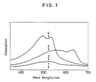
- Unpolymerized diacetylene, incompletely polymerized polydiacetylene and completely polymerized polydiacetylene can be distinguished based on the visible light absorption spectrum of the built-up layer transferred to the substrate.
- Figure 1 shows a comparison of the absorption spectra for an unpolymerized built-up film, an incompletely polymerized built-up film and a completely polymerized built-up film in the case of using 10, 12-heptacosadiynic acid.
- the spectrum 1 is that for an unpolymerized built-up film, the spectra 2 and 3 are for incompletely polymerized built-up films and spectrum 4 is for a completely polymerized built-up film.
- the difference between the spectra 2 and 3 is the result of a difference in the surface pressure at the time the irradiation with ultraviolet rays was conducted on the water surface.
- absorption was exhibited in the vicinity of 590 nm and 650 nm (spectrum 3)
- absorption was exhibited in the vicinity of 490 nm and 530 nm (spectrum 2).
- spectrum 4 for the completely polymerized built-up film and spectrum 2 is the spectrum absorption intensity, and it will be noted that the spectrum absorption intensity for the incompletely polymerized built-up film is considerably lower than that for the completely polymerized built-up layer.
- the incompletely polymerized polydiacetylene spread on the water surface at a prescribed surface pressure is transferred to a substrate to form a built-up film.
- the surface pressure ( ⁇ ) range is preferably not more than 80 dyne/cm. When the surface pressure exeeds 80 dyne/cm, the spread film disintegrates and no longer exits as a monolayer. On the other hand, the surface pressure may be low within the range in which an effective monolayer is formed.
- the absorption spectrum indicative of the degree of polymerization varies depending on the surface pressure.
- the conventional methods can be applied as regards both the types of substrate on which the diacetylene can be built up and the method of transfer used.
- the pressure at the time of building up the incompletely polymerized film in the case where incomplete polymerization was carried out at a low surface pressure, the pressure should preferably be increased in order to increase the packing density, and in the case where incomplete polymerization was carried out at high surface pressure, the pressure should be left as is since the packing density is already high.
- the built-up layer consists, for example, for a structure in which the first layer (the undermost monolayer) has its hydrophilic groups directed toward the substrate, a structure in which teh first layer (the undermost monolayer) has its hydrophobic groups directed toward the substrate, a structure in which the first and other odd numbered layers of the built-up film have their hydrophilic groups directed toward the substrate side and the second and other even numbered layers have their hydrophobic groups directed toward the substrate side, or a structure in which the first and other odd numbered layers of the built-up film have their hydrophobic groups directed toward the substrate side and the second and other even numbered layers have their hydrophilic groups directed toward the substrate side.
- the number of built-up layers is preferably between one and one hundred.
- the film built-up by transferring incompletely polymerized diacetylene compounds onto a substrate is converted into a thin film of polydiacetylene by subjecting it to an adequate amount of ultraviolet irradiation.
- the complete polymerization can be carried out by irradiation with an electron beam in a vacuum.
- the processing for completing polymelrization conducted by irradiation with ultraviolet rays or an electron beam can be carried out either with respect to the entire area of the incompletely polymerized film or with respect to selected parts of the total area thereof in the form of a desired pattern.
- the method of producing a thin film of polydiacetylene compounds according to the present method is characterized in that it comprises two stages of polymerization: a first stage in which a diacetylene compound spread into a film at a prescribed surface pressure is incompletely polymerized and a second stage in which the spread film of incompletely polymerized diacetylene compound is, after having been transferred to a substrate, converted into a completely polymerized film.
- the method of the present invention reduces the amount of morphological change in the thin built-up film resulting from structural change at the time of polymerization and enables a decrease in the number of defects in the obtained thin film.
- the electrical resistance of the thin film in the direction of thickness is increased and the chemical protection performance thereof is enhanced.
- the built-up film of the incompletely polymerized diacetylene compound produced in the course of the process of the invention is soluble in some solvents so that after lithographic patterning has been conducted by irradiation with ultraviolet rays or an electron beam for complete polymerization, the incompletely polymerized portions remaining at the regions can be dissolved away to obtain the desired pattern.
- the polydiacetylene film according to the invention serves as a protective film.
- the contat electrodes of the device are provided on the substrate before the aforesaid polydiacetylene compound thin film is formed thereon or the contat electrodes are provided on the device after conducting patterned irradiation and then removing the incompletely polymerized portions of the thin film of polydiacetylene compounds.
- the surface of the semiconductors is subjected to cleaning beforehand.
- this cleaning pretreatment is carried out to free the surface of the semiconductor substrate from native oxides and excess tellurium arising in the device fabrication process and thus to enhance the adherence between the thin film of polydiacetylene compound and the substrate.
- the surface of the compound semiconductors can be mechanically polished or chemically etched, or mechanically polished and then chemically etched.
- aqueous solution for example, a acetic acid-acetate buffer solution or a phosphoric acid-phosphate buffer solution deaerated with an inert gas such as Ar or N2.
- the reduction potential used is -0.2 to -1.0 V in the case of using a silver-silver chloride reference electrode and the reduction is continued until the current density falls to or below 1 ⁇ A/cm2.
- the electrochemical cathodic reduction of the mercury cadmium telluride or cadmium telluride substrate following mechanical polishing and/or chemical etching thereof and the method of producing a polydiacetylene compound thin film according to this invention facilitate the building up of a polydiacetylene compound thin film, enable formation of a chemically stable insulating film having a high electrical resistance without damage to the substrate, and enhance the electrial characteristics of the semiconductor device concerned.
- 10,12-heptacosadiynic acid selected as the diacetylene compound was dissolved in chloroform and this diacetylene compound solution was dripped onto a water surface using a Langmuir-Blodgett apparatus to obtain a spread film. The chloroform was then evaporated off.
- the surface pressure was adjusted to 5 dyne/cm and ultraviolet rays were irradiated onto the spread film surface at 60 mW/cm2 for 30 sec, whereby there was obtained an incompletely polymerized spread film of 10,12-heptacosadiynic acid.
- the surface pressure had been adjusted to 35 dyne/cm, five layers of the spread film were built up on a glass substrate having an Al contact electrode evaporated thereon, with the substrate transfer velocity set at 2 mm/min for the first layer and 12 mm/min for the further layers.
- the measured absorption spectrum is shown in Figure 1 (3).
- the substrate was again irradiated with ultraviolet rays, at 60 mW/cm2 for 30 min, whereby there was obtained a thin film of completely polymerized polydiacetylene compounds.
- a second Al contact electrode was evaporated on the so-obtained thin film and the electrical resistance between the two electrodes was evaluated to be 1016 ⁇ cm, thus confirming the high insulating property of the thin film.
- 10,12-heptacosadiynic acid was dissolved in chloroform and the resulting solution of a diacetylene compound was dripped onto a water surface using a Langmuir-Blodgett apparatus to obtain a spread film. The chloroform was then evaporated off.
- the spread film surface was irradiated with ultraviolet rays at 60 mW/cm2 for 5 min.
- Twenty layers of the resulting incompletely polymerized thin film of 10,12-heptacosadiynic acid were then built up on a glass substrate, with the substrate transfer velocity at 2 mm/min for the first layer and 12 mm/min for the further layers.
- the measured absorption spectrum is shown in Figure 1 (2).
- the substrate was then pattern-wise irradiated with ultraviolet rays, at 60 mW/cm2 for 30 min. It was then immersed in a chloroform solution to remove the incompletely polymerized portions and obtain a patterned thin film of good quality.
- Example 2 Twenty layers of incompletely polymerized 10,12-heptacosadiynic acid were built up on a glass substrate by the method of Example 1. The substrate was then placed in an equipment vacuumized to 10 ⁇ 8 Torr and subjected to pattern-wise irradiation with an electron beam. It was then immersed in a chloroform solution to remove the incompletely polymerized portions and obtain a patterned thin film of good quality.
- a single crystal substrate of n-type Hg 0.8 Cd 0.2 Te was mechanically polished, then chemically etched with a methanol solution containing 1% of bromine, and then immersed in a pH 5.0 acetic acid-acetate buffer solution deaerated with N2 and subjected to electrochemical cathodic reduction using a silver-silver chloride reference electrode and a platinum counter electrode, with potential sweeping rate at -5 mV/sec from the rest potential to -0.8 V, and with holding at -0.8 V until the current density fell to or below 1 ⁇ A/cm2.
- the resulting substrate was washed and dried, whereafter indium was evaporated thereon to form contact electrodes with an area therebetween of 0.36mm2.
- 10,12-heptacosadiynic acid selected as the diacetylene compound was dissolved in chloroform and this diacetylene compound solution was dripped onto a water surface using a Langmuir-Blodgett apparatus to obtain a spread film.
- the chloroform was then evaporated off, the surface pressure was adjusted to 35 dyne/cm, and ultraviolet rays were irradiated onto the spread film surface at 60 mW/cm2 for 5 min, whereby there was obtained an incompletely polymerized spread film of 10,12-heptacosadiynic acid.
- the substrate was then subjected to pattern-wise iradiation with ultraviolet rays at 60 mW/cm2 for 30 min, through a mask that prevented irradiation of the contact electrode regions.
- the remaining incompletely polymerized portions were dissolved away with chloroform.
- 10,12-heptacosadiynic acid was dissolved in chloroform and the resulting solution of the diacetylene compound was dripped onto a water surface using a Langmuir-Blodgett apparatus to obtain a spread film. The chloroform was then evaporated off.
- a single crystal substrate of n-type Hg 0.8 Cd 0.2 Te was mechanically polished, then chemically etched with a methanol solution containing 1% of bromine, and then immersed in a pH 5.0 acetic acid-acetate buffer solution deaerated with N2 and subjected to electrochemical cathodic reduction using a silver-silver chloride reference electrode and a platinum counter electrode, with sweeping rate at -5 mV/sec from the rest potential and -0.8 V and with holding the potential at -0.8 V until the current density fell to or below 1 ⁇ A/cm2 .
- the resulting substrate was washed and dried, whereafter indium was evaporated thereon to form contact electrodes with an area therebetween of 0.36mm2.
- the substrate was then irradiated with ultraviolet rays at 60 mW/cm2 for 30 min, through a mask that prevented irradiation of the electrode regions.
- ultraviolet rays at 60 mW/cm2 for 30 min
- a mask that prevented irradiation of the electrode regions.
- the unirradiated portions were dissolved away with chloroform.
- the infrared ray response characteristics of the resulting device were examined in the same way as described in Example 4. The device exhibited defects in the film at an output of a mere 4 ⁇ V and was unsuitable for practical application.
- a single crystal substrate of n-type Hg 0.8 Cd 0.2 Te was mechanically polished and then chemically etched with a methanol solution containing 1% of bromine. After the substrate had been washed and dried, indium was vapor deposited thereon to form electrodes with an area therebetween of 0.36mm2 Next 10,12-heptacosadiynic acid was dissolved in chloroform and this diacetylene compound solution was dripped onto a water surface using a Langmuir-Blodgett apparatus to obtain a spread film.
- the chloroform was then evaporated off, the surface pressure was adjusted to 35 dyne/cm, and fifteen layers of the spread film were built up on the aforesaid semiconductor substrate provided with electrodes, with the substrate transfer velocity set at 2 mm/min for the first layer and 12 mm/min for the further layers.
- This substrate was then subjected to pattern-wise irradiation with ultraviolet rays at 60 mW/cm2 for 30 min, through a mask that prevented irradiation of the electrode regions. As a result, there was formed a thin film of polydiacetylene compound at all parts of the substrate other than the electrode regions.
- the infrared ray response characteristics of the resulting device were examined in the same way as described in Example 4. While the resistance of the substrate was found to vary between 4.2 ⁇ at room temperature and 24 ⁇ at 77 K, it was unresponsive to light and was not suitable for practical application.
- the invention when the invention is applied to build up a thin film of polydiacetylene compound on a mercury cadmium telluride or cadmium telluride semiconductor substrate which has been subjected to electrochemical cathode processing beforehand, the resulting thin film can serve as a passivation film and as a result it is possible to realize a semiconductor device exhibiting excellent electrical characteristics.
Landscapes
- Physics & Mathematics (AREA)
- Spectroscopy & Molecular Physics (AREA)
- General Physics & Mathematics (AREA)
- Addition Polymer Or Copolymer, Post-Treatments, Or Chemical Modifications (AREA)
- Liquid Deposition Of Substances Of Which Semiconductor Devices Are Composed (AREA)
- Electroluminescent Light Sources (AREA)
- Formation Of Insulating Films (AREA)
- Manufacture Of Macromolecular Shaped Articles (AREA)
Applications Claiming Priority (6)
| Application Number | Priority Date | Filing Date | Title |
|---|---|---|---|
| JP183437/87 | 1987-07-24 | ||
| JP18343787 | 1987-07-24 | ||
| JP29502287 | 1987-11-25 | ||
| JP295022/87 | 1987-11-25 | ||
| JP141483/87 | 1988-06-10 | ||
| JP63141483A JPH01236207A (ja) | 1987-07-24 | 1988-06-10 | ポリジアセチレン薄膜の製造法 |
Publications (3)
| Publication Number | Publication Date |
|---|---|
| EP0300728A2 true EP0300728A2 (de) | 1989-01-25 |
| EP0300728A3 EP0300728A3 (en) | 1990-01-17 |
| EP0300728B1 EP0300728B1 (de) | 1993-09-29 |
Family
ID=27318258
Family Applications (1)
| Application Number | Title | Priority Date | Filing Date |
|---|---|---|---|
| EP88306586A Expired - Lifetime EP0300728B1 (de) | 1987-07-24 | 1988-07-19 | Polydiacetylen-Dünnschicht-Herstellungsverfahren |
Country Status (4)
| Country | Link |
|---|---|
| US (1) | US4906550A (de) |
| EP (1) | EP0300728B1 (de) |
| JP (1) | JPH01236207A (de) |
| DE (1) | DE3884502T2 (de) |
Cited By (2)
| Publication number | Priority date | Publication date | Assignee | Title |
|---|---|---|---|---|
| EP0385656A3 (de) * | 1989-02-27 | 1991-11-06 | Matsushita Electric Industrial Co., Ltd. | Verfahren zur Herstellung eines hoch orientierten ultralangen konjugierten Polymers |
| EP0385506A3 (de) * | 1989-03-03 | 1991-11-13 | Matsushita Electric Industrial Co., Ltd. | Herstellung einer organischen Membrane |
Families Citing this family (8)
| Publication number | Priority date | Publication date | Assignee | Title |
|---|---|---|---|---|
| JPH04173841A (ja) * | 1990-11-05 | 1992-06-22 | Nec Corp | 機能性基を有する高分子膜の部分的形成方法 |
| JP3138442B2 (ja) * | 1997-12-26 | 2001-02-26 | 株式会社ホギメディカル | ポリジアセチレン膜を用いる発色センサー |
| US6194529B1 (en) * | 1999-03-19 | 2001-02-27 | Board Of Trustees Operating Michigan State University | Ordered polyacetylenes and process for the preparation thereof |
| KR100663713B1 (ko) * | 2005-12-16 | 2007-01-03 | 성균관대학교산학협력단 | 신규한 폴리디아세틸렌 초분자체 색 전이 센서 |
| JP2011503517A (ja) * | 2006-11-13 | 2011-01-27 | アテリス テクノロジーズ,エルエルシー | 農薬バイオマーカー |
| JP2011511930A (ja) * | 2007-11-14 | 2011-04-14 | アテリス テクノロジーズ,エルエルシー | バイオマーカー検出 |
| JP5257744B2 (ja) * | 2008-03-17 | 2013-08-07 | 株式会社リコー | ポリジアセチレンを半導体層とする有機薄膜トランジスタの製造方法 |
| JP6292242B2 (ja) * | 2016-01-27 | 2018-03-14 | 岩崎電気株式会社 | 硬化方法、及び硬化システム |
Family Cites Families (8)
| Publication number | Priority date | Publication date | Assignee | Title |
|---|---|---|---|---|
| US4291118A (en) * | 1979-12-26 | 1981-09-22 | W. R. Grace & Co. | Relief imaging liquids |
| JPS58111029A (ja) * | 1981-12-24 | 1983-07-01 | Kureha Chem Ind Co Ltd | ジアセチレン化合物累積膜の製造方法 |
| US4562141A (en) * | 1982-09-29 | 1985-12-31 | Ciba Geigy Corporation | Polymerisable composition comprising conjugated diacetylenic compounds, material coated therewith and the use thereof |
| GB8308309D0 (en) * | 1983-03-25 | 1983-05-05 | Qmc Ind Res | Information holding device |
| US4528261A (en) * | 1983-03-28 | 1985-07-09 | E. I. Du Pont De Nemours And Company | Prelamination, imagewise exposure of photohardenable layer in process for sensitizing, registering and exposing circuit boards |
| JPS621701A (ja) * | 1985-06-28 | 1987-01-07 | Toshiba Corp | 有機超薄膜の製造方法 |
| US4721769A (en) * | 1985-10-18 | 1988-01-26 | Gte Laboratories Incorporated | Diacetylene segmented copolymers |
| US4830952A (en) * | 1987-11-06 | 1989-05-16 | Eastman Kodak Company | Langmuir-Blodgett film assembly |
-
1988
- 1988-06-10 JP JP63141483A patent/JPH01236207A/ja active Granted
- 1988-07-19 DE DE88306586T patent/DE3884502T2/de not_active Expired - Fee Related
- 1988-07-19 EP EP88306586A patent/EP0300728B1/de not_active Expired - Lifetime
- 1988-07-25 US US07/224,011 patent/US4906550A/en not_active Expired - Fee Related
Non-Patent Citations (1)
| Title |
|---|
| MAKROMOL. CHEM., vol. 180, 1979, pages 1787-1795; V. ENKELMANN et al.: "Investigation of the topochemical solid-state polymerization of a diacetylene by X-ray methods and Brillouin-spectroscopy" * |
Cited By (2)
| Publication number | Priority date | Publication date | Assignee | Title |
|---|---|---|---|---|
| EP0385656A3 (de) * | 1989-02-27 | 1991-11-06 | Matsushita Electric Industrial Co., Ltd. | Verfahren zur Herstellung eines hoch orientierten ultralangen konjugierten Polymers |
| EP0385506A3 (de) * | 1989-03-03 | 1991-11-13 | Matsushita Electric Industrial Co., Ltd. | Herstellung einer organischen Membrane |
Also Published As
| Publication number | Publication date |
|---|---|
| EP0300728B1 (de) | 1993-09-29 |
| US4906550A (en) | 1990-03-06 |
| DE3884502T2 (de) | 1994-04-28 |
| DE3884502D1 (de) | 1993-11-04 |
| EP0300728A3 (en) | 1990-01-17 |
| JPH01236207A (ja) | 1989-09-21 |
| JPH0570509B2 (de) | 1993-10-05 |
Similar Documents
| Publication | Publication Date | Title |
|---|---|---|
| US5314772A (en) | High resolution, multi-layer resist for microlithography and method therefor | |
| EP1007349B1 (de) | Leitende gemusterte polymeroberfläche, verfahren zu ihrer herstellung und diese enthaltende anordnungen | |
| EP0300728B1 (de) | Polydiacetylen-Dünnschicht-Herstellungsverfahren | |
| CN115148890B (zh) | 一种基于金属掩膜的铌铝约瑟夫森结的制备方法 | |
| Angelopoulos et al. | Water soluble polyanilines: properties and applications | |
| KR20040047978A (ko) | 전기 전도성이 있는 폴리머의 패턴형성방법 | |
| US4214966A (en) | Process useful in the fabrication of articles with metallized surfaces | |
| US7001849B2 (en) | Surface treatment and protection method for cadmium zinc telluride crystals | |
| US4548893A (en) | High resolution lithographic resist and method | |
| Angelopoulos et al. | Conducting polymers as lithographic materials | |
| JP2883798B2 (ja) | 半導体素子のパターン化方法 | |
| US4702993A (en) | Treatment of planarizing layer in multilayer electron beam resist | |
| US5269890A (en) | Electrochemical process and product therefrom | |
| EP0395426B1 (de) | Bildherstellungsverfahren mittels einer elektrisch leitfähigen Zusammensetzung | |
| US3402073A (en) | Process for making thin film circuit devices | |
| RU2080693C1 (ru) | Способ формирования пленочных микромостиков из высокотемпературных сверхпроводников | |
| US4835083A (en) | Method for patterning electroconductive film and patterned electroconductive film | |
| JPS62142323A (ja) | X線ホトリソグラフイに使用するマスクの加法的方法及びその結果得られるマスク | |
| US5306601A (en) | Fine pattern forming material and pattern forming method | |
| US4810617A (en) | Treatment of planarizing layer in multilayer electron beam resist | |
| US4027052A (en) | Fabrication of iron oxide pattern | |
| US4595649A (en) | Glassy TiO2 polymer films as electron beam charge dissipation layers | |
| JP2564030B2 (ja) | 電気化学測定用カーボン薄膜電極の製造方法 | |
| RU2687501C1 (ru) | Способ изготовления фотоэлектрического преобразователя с антиотражающим покрытием | |
| US4476216A (en) | Method for high resolution lithography |
Legal Events
| Date | Code | Title | Description |
|---|---|---|---|
| PUAI | Public reference made under article 153(3) epc to a published international application that has entered the european phase |
Free format text: ORIGINAL CODE: 0009012 |
|
| AK | Designated contracting states |
Kind code of ref document: A2 Designated state(s): DE FR GB |
|
| PUAL | Search report despatched |
Free format text: ORIGINAL CODE: 0009013 |
|
| AK | Designated contracting states |
Kind code of ref document: A3 Designated state(s): DE FR GB |
|
| 17P | Request for examination filed |
Effective date: 19900509 |
|
| 17Q | First examination report despatched |
Effective date: 19921119 |
|
| GRAA | (expected) grant |
Free format text: ORIGINAL CODE: 0009210 |
|
| AK | Designated contracting states |
Kind code of ref document: B1 Designated state(s): DE FR GB |
|
| REF | Corresponds to: |
Ref document number: 3884502 Country of ref document: DE Date of ref document: 19931104 |
|
| ET | Fr: translation filed | ||
| PLBE | No opposition filed within time limit |
Free format text: ORIGINAL CODE: 0009261 |
|
| STAA | Information on the status of an ep patent application or granted ep patent |
Free format text: STATUS: NO OPPOSITION FILED WITHIN TIME LIMIT |
|
| 26N | No opposition filed | ||
| PGFP | Annual fee paid to national office [announced via postgrant information from national office to epo] |
Ref country code: FR Payment date: 19960709 Year of fee payment: 9 |
|
| PGFP | Annual fee paid to national office [announced via postgrant information from national office to epo] |
Ref country code: GB Payment date: 19960710 Year of fee payment: 9 |
|
| PGFP | Annual fee paid to national office [announced via postgrant information from national office to epo] |
Ref country code: DE Payment date: 19960726 Year of fee payment: 9 |
|
| PG25 | Lapsed in a contracting state [announced via postgrant information from national office to epo] |
Ref country code: GB Free format text: LAPSE BECAUSE OF NON-PAYMENT OF DUE FEES Effective date: 19970719 |
|
| GBPC | Gb: european patent ceased through non-payment of renewal fee |
Effective date: 19970719 |
|
| PG25 | Lapsed in a contracting state [announced via postgrant information from national office to epo] |
Ref country code: FR Free format text: LAPSE BECAUSE OF NON-PAYMENT OF DUE FEES Effective date: 19980331 |
|
| PG25 | Lapsed in a contracting state [announced via postgrant information from national office to epo] |
Ref country code: DE Free format text: LAPSE BECAUSE OF NON-PAYMENT OF DUE FEES Effective date: 19980401 |
|
| REG | Reference to a national code |
Ref country code: FR Ref legal event code: ST |