EP0300826A2 - Digitaler Datendetektor - Google Patents
Digitaler Datendetektor Download PDFInfo
- Publication number
- EP0300826A2 EP0300826A2 EP88306788A EP88306788A EP0300826A2 EP 0300826 A2 EP0300826 A2 EP 0300826A2 EP 88306788 A EP88306788 A EP 88306788A EP 88306788 A EP88306788 A EP 88306788A EP 0300826 A2 EP0300826 A2 EP 0300826A2
- Authority
- EP
- European Patent Office
- Prior art keywords
- phase
- point
- sampling point
- current sampling
- data
- Prior art date
- Legal status (The legal status is an assumption and is not a legal conclusion. Google has not performed a legal analysis and makes no representation as to the accuracy of the status listed.)
- Granted
Links
- 238000005070 sampling Methods 0.000 claims abstract description 175
- 238000010586 diagram Methods 0.000 description 8
- 238000006467 substitution reaction Methods 0.000 description 6
- 230000001934 delay Effects 0.000 description 3
- 238000000034 method Methods 0.000 description 3
- 238000000605 extraction Methods 0.000 description 2
- 230000005415 magnetization Effects 0.000 description 2
- 230000005540 biological transmission Effects 0.000 description 1
- 238000006243 chemical reaction Methods 0.000 description 1
- 230000000295 complement effect Effects 0.000 description 1
- 230000003111 delayed effect Effects 0.000 description 1
- 238000001514 detection method Methods 0.000 description 1
- 230000001360 synchronised effect Effects 0.000 description 1
Images
Classifications
-
- G—PHYSICS
- G11—INFORMATION STORAGE
- G11B—INFORMATION STORAGE BASED ON RELATIVE MOVEMENT BETWEEN RECORD CARRIER AND TRANSDUCER
- G11B20/00—Signal processing not specific to the method of recording or reproducing; Circuits therefor
- G11B20/10—Digital recording or reproducing
- G11B20/10009—Improvement or modification of read or write signals
- G11B20/10046—Improvement or modification of read or write signals filtering or equalising, e.g. setting the tap weights of an FIR filter
- G11B20/10203—Improvement or modification of read or write signals filtering or equalising, e.g. setting the tap weights of an FIR filter baseline correction
-
- G—PHYSICS
- G11—INFORMATION STORAGE
- G11B—INFORMATION STORAGE BASED ON RELATIVE MOVEMENT BETWEEN RECORD CARRIER AND TRANSDUCER
- G11B20/00—Signal processing not specific to the method of recording or reproducing; Circuits therefor
- G11B20/10—Digital recording or reproducing
- G11B20/10009—Improvement or modification of read or write signals
-
- G—PHYSICS
- G11—INFORMATION STORAGE
- G11B—INFORMATION STORAGE BASED ON RELATIVE MOVEMENT BETWEEN RECORD CARRIER AND TRANSDUCER
- G11B20/00—Signal processing not specific to the method of recording or reproducing; Circuits therefor
- G11B20/10—Digital recording or reproducing
- G11B20/10009—Improvement or modification of read or write signals
- G11B20/10037—A/D conversion, D/A conversion, sampling, slicing and digital quantisation or adjusting parameters thereof
-
- G—PHYSICS
- G11—INFORMATION STORAGE
- G11B—INFORMATION STORAGE BASED ON RELATIVE MOVEMENT BETWEEN RECORD CARRIER AND TRANSDUCER
- G11B20/00—Signal processing not specific to the method of recording or reproducing; Circuits therefor
- G11B20/10—Digital recording or reproducing
- G11B20/10527—Audio or video recording; Data buffering arrangements
Definitions
- the present invention relates generally to digital data detectors, and more particularly, to digital data detectors for detecting digital data from a digital modulation signal in a digital data transmission system.
- a digital data detecting apparatus is disclosed in Japanese Patent Laying-Open Gazette No. 92410/1984.
- This apparatus detects digital data from a digital modulation signal in the following manner.
- the digital modulation signal is sampled at a frequency of m times (m > 1) a channel bit rate. It is assumed that the digital modulation signal is sampled at a frequency of two times a channel bit rate.
- Sampling data S i+1 at the current sampling point and sampling data S i at a sampling point which is located one point before the current sampling point are used to find a phase interval P between a point at which the digital modulation signal crosses a reference level and the current sampling point from the following equation.
- phases of sampling points are represented by values of 0 to N-1 obtained by dividing a channel bit period into N equal divisions; where N/2 is a value of one-half of a channel bit interval.
- a predetermined value (N/2) is added to a phase P i of the sampling point which is located one point before the current sampling point, to obtain an estimated value of a phase of the current sampling point.
- a clock in synchronization with the digital modulation signal and digital data corresponding to the clock are detected in response to sampling data at each sampling point thus obtained and a phase of the sampling point.
- the data detecting apparatus can cope with multichannel input by sampling channels at different timing and sequentially converting the channels into signals, to be inputted.
- Japanese Patent Laying-Open Gazette No. 222072/1986 filed by the assignee of the present application discloses a digital magnetic recording and reproducing apparatus in which clock extraction is determined by comparing phase information before and behind sampling data of a reproduced signal with each other and comparing magnitudes of the phase differences calculated from the sampling data with each other and the phase information is changed depending on the result of the determination.
- An object of the present invention is to provide a digital data detector in which data is little erroneously detected even if fluctuations in the frequency increase.
- the digital data detector comprises sampling data detecting means, phase interval calculating means, phase calculating means, clock detecting means and data detecting means.
- the sampling data detecting means samples a digital modulation signal at a constant frequency.
- the phase interval calculating means is responsive to sampling data detected by the sampling data detecting means for calculating a phase interval between a point at which a digital modulation signal crosses a reference level and the current sampling point.
- the phase calculating means is responsive to a phase of a sampling point which is located one point before and a phase of a sampling point which is located at least two points before the current sampling point for calculating a phase of the current sampling point.
- the clock detecting means is responsive to the phase of each sampling point calculated by the phase calculating means for detecting a clock signal in synchronization with the digital modulation signal.
- the above described data detecting means is responsive to the above described phase interval, the above described phase of the current sampling point and the above described clock signal for detecting digital data from the digital modulation signal.
- the phase of the current sampling point is calculated in response to the phase of the sampling point which is located one point before and the phase of the sampling point which is located at least two points before the current sampling point.
- the phase of the current sampling point is calculated in response to the phase of the sampling point which is located one point before and the phase of the sampling point which is located at least two points before the phase of the current sampling point.
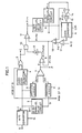
- Fig. 1 is a block diagram showing a main portion of a digital data detector according to the present invention.
- a digital modulation signal is sampled in a predetermined cycle, so that sampling data at the sampling point is detected and the position, i.e., a phase of the sampling point is calculated.
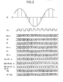
- Fig. 2 is a timing chart for explaining an operation of the digital data detector.
- a digital modulation signal S is inputted to an A/D converter 1.
- the A/D converter 1 samples the digital modulation signal S in synchronization with a clock signal f s , to convert the same into M-bit digital data.
- the frequency of the clock signal f s is m times a channel bit rate. It is assumed that the frequency of the clock signal f s is two times the channel bit rate.
- the polarities of plus (+) and minus (-) of the digital modulation signal are represented by an MSB (Most Significant Bit) of "0" and "1" using complement on, for example, two.
- An output of the A/D converter 1 is inputted to an M-bit parallel delay circuit 2, a zero data detecting circuit 4 and an absolute value circuit 5 as sampling data (referred to as the current data hereinafter) S i+1 at the current sampling point.
- An output of the M-bit parallel delay circuit 2 is inputted to an absolute value circuit 6 as sampling data (referred to as the preceding data hereinafter) S i at a sampling point which is located one point before the current sampling point.
- the zero data detecting circuit 4 outputs "1" when the current data S i+1 is "0" and the preceding data has negative polarity, i.e., the MSB is "1", which otherwise would output the MSB of the current data S i+1 .
- An output of the zero data detecting circuit 4 is applied to one input terminal of an exclusive OR gate (referred to as an Ex-OR gate hereinafter) 3.
- the MSB of the preceding data S i outputted from the M-bit parallel delay circuit 2 is applied to the other input terminal of the Ex-OR gate 3.
- the Ex-OR gate 3 outputs "1" when input signals applied to both the input terminals are different from each other while outputting "0" when the input signals are the same.
- the current data S i+1 being "0" (i.e., the sampling point being on the zero level)
- the current data S i+1 and the preceding data S i are the same in polarity when the preceding data S i has negative polarity while the current data S i+1 and the succeeding data are different in polarity when the succeeding data has positive polarity.
- the current data S i+1 being "0"
- the current data S i+1 and the preceding data S i are the same in polarity when the preceding data S i has positive polarity while the current data S i+1 and the succeeding data are different in polarity when the succeeding data has negative polarity.
- the current data S i+1 and the preceding data S i are converted into absolute values
- the arithmetic circuit 7 calculates a phase interval P between a zero level crossing and the sampling point of the current data S i from the following equation using the absolute value
- phases of sampling points are represented by values of 0 to N-1 obtained from dividing a channel bit period into N equal divisions, where N/2 represents the position of the zero level crossing.
- a calculating method of the phase interval P using the equation (4) is employed in the digital magnetic recording and reproducing apparatus disclosed in the above described Japanese Patent Laying-Open Gazette No. 222072/1986.
- the calculated phase interval P is compared with an output (P i + Pd) of a phase loop (as described below) by a comparator 8, the result of comparison being outputted as ⁇ P - (P i + Pd) ⁇ .
- the output ⁇ P - (P i + Pd) ⁇ of the comparator 8 is corrected in numerical value by a coefficient K (0 ⁇ K ⁇ 1) of a constant multiplier 9 corresponding to loop gain, to be outputted as ⁇ P - (P i + Pd) ⁇ K.
- the output ⁇ P - (P i + Pd) ⁇ K of the constant multiplier 9 is applied to one input terminal of a logical product gate (referred to as AND gate hereinafter) 10.
- the AND gate 10 has another input terminal receiving an output C of the above described Ex-OR gate 3. Consequently, only when the digital modulation signal S crosses the zero level so that the output C of the Ex-OR gate 3 becomes "1", the output ⁇ P - (P i + Pd) ⁇ K of the constant multiplier 9 is outputted from the AND gate 10, to be applied to one input terminal of an adder 11.
- the adder 11 has another input terminal receiving an output (P i + Pd) of the phase loop. The result of addition by the adder 11 becomes a phase P i+1 of the current sampling point.
- the number of delays of the I-bit parallel delay circuit 13 is two.
- An output of the I-bit parallel delay circuit 13 becomes a phase P i-2 of a sampling point which is located three points before the current sampling point.
- the output P i-2 of the I-bit parallel delay circuit 13 is inputted to the other input terminal of the comparator 14, to be compared with the output P i of the above described J-bit parallel delay circuit 12.
- An output of the comparator 14 becomes (P i - P i-2 ).
- the output (P i - P i-2 ) is inputted to a constant multiplier 15 having a coefficient L (0 ⁇ L ⁇ 1) and corrected in numerical value, to be outputted as (P i - P i
- the output (P i - P i-2 ) ⁇ L of the constant multiplier 15 is applied to a data converter 16.
- the data converter 16 compares an input signal with a predetermined value Lim, to output a value A previously set when the following condition is satisfied while directly outputting the input signal when the following condition is not satisfied: (P i - P i-2 ) ⁇ L ⁇ Lim or (P i - P i-2 ) ⁇ L ⁇ -Lim
- the data converter 16 is provided for the following reasons. More specifically, when input data becomes invalid due to burst generation or the like, the phase calculated based on the input data also becomes invalid, so that the difference (P i - P i-2 ) between the two phases exceeds a range of a normal value. Since this affects the subsequent calculation of phases, the return to the normal value is delayed. When the value of (P i - P i-2 ) ⁇ L is outside a predetermined range, the value is replaced with a value previously set.
- An output of the data detector 16 is applied to one input terminal of an adder 17.
- the adder 17 has another input terminal receiving a signal corresponding to N/2.
- the output Pd of the adder 17 is applied to the other input terminal of the adder 18. Since the phase P i of the the sampling point which is located one point before the current sampling point is applied to one input terminal of the adder 18 as described above, (P i + Pd) is outputted from the adder 18.
- the output (P i + Pd) is applied to the other input terminal of the adder 11 as an output of the phase loop, i.e., an estimated value of the phase of the current sampling point.
- the output of the AND gate 10 is applied to one input terminal of the adder 11.
- P denotes a phase interval between a zero level crossing and the current sampling point, which is calculated from the equation (4).
- P i+1 denotes a phase of the current sampling point
- P i denotes a phase of a sampling point which is located one point before the current sampling point
- P i denotes a phase of a sampling point which is located three points before the current sampling point
- N/2 denotes a value showing half of the channel bit interval
- K and L denote coefficients.
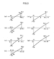
- Fig. 3 is a diagram for explaining clock detection determining criteria according to the present embodiment.
- Figs. 3(a) to 3(d) show a case in which one ⁇ point (a point of N/2 from the zero point) of the digital modulation signal S exists between P i and P i+1
- Figs. 3(e) to 3(g) show a case in which the above described ⁇ point does not exist between P i and P i+1 .
- a clock in synchronization with the digital modulation signal is extracted by a circuit shown in Fig. 4 as described below.
- data corresponding to this clock is detected by the following condition.
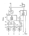
- Fig. 4 is a block diagram showing structure of circuits for detecting a clock and data based on the above described clock detecting criteria and the data determining condition.
- a phase P i of a sampling point which is located one point before the current sampling point, a phase P i+1 of the current sampling point and a phase interval P are applied to latch circuits 21, 22 and 23, respectively.
- the latch circuits 21, 22 and 23 hold P i , P i+1 and P at timing of a sampling frequency f s , to output the same.
- An output of the latch circuit 21 is applied to one input terminal of a comparator 24 and one input terminal of a comparator 25.
- An output of the latch circuit 22 is applied to the other input terminal of the comparator 25, one input terminal of a comparator 26 and one input terminal of a subtracter 27.
- a signal corresponding to N/2 is applied to the other input terminals of the comparator 24, the comparator 26 and the subtracter 27.
- the comparator 24 compares P i with N/2.
- the comparator 25 compares P i with P i+1 .
- the comparator 26 compares P i+1 with N/2.
- Outputs of the comparators 24, 25 and 26 and the output C of the Ex-OR gate 3 are applied to a clock detecting circuit 28.
- the clock detecting circuit 28 outputs "1" when the above described clock detecting conditions are satisfied while outputting "0" when the clock detecting conditions are not satisfied.
- An output of the clock detecting circuit 28 is inputted to a data input terminal D of a flip-flop 29, to be acquired at timing of f s .
- An output of the flip-flop 29 is applied to one input terminal of an AND gate 30.
- the AND gate 30 has another input terminal receiving f s . When both the input signals are "1", the AND gate 30 outputs "1" at timing of f s , so that the output signal becomes a clock CK.
- an output corresponding to ⁇ P i+1 - (N/2) ⁇ is derived from the subtracter 27, the output being applied to one input terminal of a comparator 31.
- the comparator 31 has another input terminal receiving an output of the latch circuit 23.
- the comparator 31 outputs "1" when P > P i+1 - N/2, which otherwise would output "0".
- An output R of the comparator 31, a signal representing the sign of the preceding data S i , i.e., an MSB of S i and the output C of the Ex-OR gate 3 are inputted to a data detecting circuit 32.
- the data detecting circuit 32 samples data in response to the inputted signal based on the above described data determining condition.
- the data detecting circuit 32 generally outputs the sign of the sampling data S i as reproduced data while outputting the sign of the sampling data S i+1 , i.e., a signal obtained by inverting S i as reproduced data when the output C of the Ex-OR gate 3 is ''1'' and the output R of the comparator 31 is "1" (when the relation P > P i+1 - N/2 is satisfied).
- An output of the data detecting circuit 32 is inputted to a data input terminal D of a flip-flop 33 and outputted from the flip-flop 33 at timing of the clock CK, so that reproduced data D0 synchronized with the clock CK is detected.
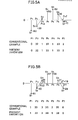
- Figs. 5A and 5B are diagrams in which the phase calculated by the digital data detector according to the present embodiment is compared with the phase calculated by the conventional data detecting apparatus.
- Fig. 5A shows a case in which fluctuations in the frequency of the digital modulation signal are small
- Fig. 5B shows a case in which fluctuations in the frequency of the digital modulation signal are large.
- a sampling point S4 is described by way of example. In this case, there is no point at which the digital modulation signal S and the reference level (zero level) crosses each other between sampling points S3 and S4.
- the equation (3) and the equations (6) and (7) are used in the conventional example and the present embodiment, respectively.
- sampling point S7 is described by way of example.
- Pd (P6 - P4) ⁇ L + N/2
- P7 ⁇ P - (P6 + Pd) ⁇ K + P6 + Pd
- P6 + Pd 71, which exceeds 63.
- 64 is subtracted from 71, so that 7 is obtained.
- a reference point for obtaining the phase of each sampling point is a zero level crossing.
- the digital data is less erroneously detected.
- the channels may be sampled at different timing and the number of delays of the parallel delay circuits 2 and 12 and the number of delays of the parallel delay circuit 13 may be made Y and 2Y, respectively.
Landscapes
- Engineering & Computer Science (AREA)
- Signal Processing (AREA)
- Multimedia (AREA)
- Digital Transmission Methods That Use Modulated Carrier Waves (AREA)
- Signal Processing For Digital Recording And Reproducing (AREA)
- Synchronisation In Digital Transmission Systems (AREA)
- Stabilization Of Oscillater, Synchronisation, Frequency Synthesizers (AREA)
Applications Claiming Priority (2)
| Application Number | Priority Date | Filing Date | Title |
|---|---|---|---|
| JP182985/87 | 1987-07-22 | ||
| JP62182985A JPH069106B2 (ja) | 1987-07-22 | 1987-07-22 | ディジタルデ−タ検出器 |
Publications (3)
| Publication Number | Publication Date |
|---|---|
| EP0300826A2 true EP0300826A2 (de) | 1989-01-25 |
| EP0300826A3 EP0300826A3 (en) | 1990-05-09 |
| EP0300826B1 EP0300826B1 (de) | 1993-07-07 |
Family
ID=16127744
Family Applications (1)
| Application Number | Title | Priority Date | Filing Date |
|---|---|---|---|
| EP88306788A Expired - Lifetime EP0300826B1 (de) | 1987-07-22 | 1988-07-22 | Digitaler Datendetektor |
Country Status (5)
| Country | Link |
|---|---|
| US (1) | US4910517A (de) |
| EP (1) | EP0300826B1 (de) |
| JP (1) | JPH069106B2 (de) |
| CA (1) | CA1287882C (de) |
| DE (1) | DE3882176T2 (de) |
Cited By (6)
| Publication number | Priority date | Publication date | Assignee | Title |
|---|---|---|---|---|
| EP0546851A1 (de) * | 1991-12-13 | 1993-06-16 | Sharp Kabushiki Kaisha | Digitaler Datendetektor |
| EP0538867A3 (en) * | 1991-10-25 | 1995-09-20 | Sony Corp | Decision-directed digital phase locked loop |
| EP0664447A4 (de) * | 1993-07-12 | 1995-12-06 | Toshiba Kk | Methode und vorrichtung zur messung der phasendifferenz. |
| EP0483296B1 (de) * | 1990-03-01 | 1998-05-27 | Siemens Nixdorf Informationssysteme Aktiengesellschaft | Verfahren zum auswerten binärer informationen einer magnetspeicherkarte |
| WO1999039346A1 (en) * | 1998-01-31 | 1999-08-05 | Seagate Technology | Detection of pulse peak instance and amplitude in a storage drive |
| US6185174B1 (en) | 1998-01-31 | 2001-02-06 | Seagate Technology Llc | Disk drive system having hybrid analog/digital pulse peak instance/amplitude data detection channels |
Families Citing this family (2)
| Publication number | Priority date | Publication date | Assignee | Title |
|---|---|---|---|---|
| JP2818997B2 (ja) * | 1993-06-30 | 1998-10-30 | シャープ株式会社 | ディジタルデータ検出器 |
| CH712608A1 (de) * | 2016-06-27 | 2017-12-29 | Legic Identsystems Ag | RFID-Empfänger und Verfahren zum Extrahieren von in einem Funksignal codierten Datenbits. |
Family Cites Families (7)
| Publication number | Priority date | Publication date | Assignee | Title |
|---|---|---|---|---|
| US3946432A (en) * | 1974-10-10 | 1976-03-23 | Cbs Inc. | Apparatus for digitally encoding a television signal |
| US4204199A (en) * | 1977-11-04 | 1980-05-20 | Mca Disco-Vision, Inc. | Method and means for encoding and decoding digital data |
| JPS5992410A (ja) * | 1982-11-17 | 1984-05-28 | Sony Corp | デ−タ検出装置 |
| NL8303563A (nl) * | 1983-10-17 | 1985-05-17 | Philips Nv | Inrichting voor het weergeven van digitale informatie via een overdrachtsmedium. |
| IT1200426B (it) * | 1985-03-21 | 1989-01-18 | Honeywell Inf Systems | Apparato digitale per sistema di recupero di informazioni binarie registrate su supporti magnetici |
| JPS61222072A (ja) * | 1985-03-26 | 1986-10-02 | Sharp Corp | デイジタル磁気記録再生装置 |
| JPH0619912B2 (ja) * | 1985-06-18 | 1994-03-16 | シャープ株式会社 | デジタル磁気記録再生装置 |
-
1987
- 1987-07-22 JP JP62182985A patent/JPH069106B2/ja not_active Expired - Lifetime
-
1988
- 1988-07-20 CA CA000572540A patent/CA1287882C/en not_active Expired
- 1988-07-20 US US07/221,871 patent/US4910517A/en not_active Expired - Lifetime
- 1988-07-22 DE DE88306788T patent/DE3882176T2/de not_active Expired - Fee Related
- 1988-07-22 EP EP88306788A patent/EP0300826B1/de not_active Expired - Lifetime
Cited By (11)
| Publication number | Priority date | Publication date | Assignee | Title |
|---|---|---|---|---|
| EP0483296B1 (de) * | 1990-03-01 | 1998-05-27 | Siemens Nixdorf Informationssysteme Aktiengesellschaft | Verfahren zum auswerten binärer informationen einer magnetspeicherkarte |
| EP0538867A3 (en) * | 1991-10-25 | 1995-09-20 | Sony Corp | Decision-directed digital phase locked loop |
| EP0546851A1 (de) * | 1991-12-13 | 1993-06-16 | Sharp Kabushiki Kaisha | Digitaler Datendetektor |
| US5355392A (en) * | 1991-12-13 | 1994-10-11 | Sharp Kabushiki Kaisha | Digital data detector for reducing errors due to frequency variations |
| EP0664447A4 (de) * | 1993-07-12 | 1995-12-06 | Toshiba Kk | Methode und vorrichtung zur messung der phasendifferenz. |
| US5610527A (en) * | 1993-07-12 | 1997-03-11 | Kabushiki Kaisha Toshiba | Phase difference microwave densitometer and method which detects a number of phase rotations through a reference point |
| US5969254A (en) * | 1993-07-12 | 1999-10-19 | Kabushiki Kaisha Toshiba | Phase difference measuring apparatus and method |
| WO1999039346A1 (en) * | 1998-01-31 | 1999-08-05 | Seagate Technology | Detection of pulse peak instance and amplitude in a storage drive |
| WO2000010167A1 (en) * | 1998-01-31 | 2000-02-24 | Seagate Technology, Inc. | Detection of pulse peak instance and amplitude in a storage drive |
| US6185174B1 (en) | 1998-01-31 | 2001-02-06 | Seagate Technology Llc | Disk drive system having hybrid analog/digital pulse peak instance/amplitude data detection channels |
| US6529460B1 (en) | 1998-01-31 | 2003-03-04 | Seagate Technology Llc | Detection of pulse peak instance and amplitude in a storage drive |
Also Published As
| Publication number | Publication date |
|---|---|
| EP0300826B1 (de) | 1993-07-07 |
| JPS6425357A (en) | 1989-01-27 |
| JPH069106B2 (ja) | 1994-02-02 |
| DE3882176D1 (de) | 1993-08-12 |
| DE3882176T2 (de) | 1994-02-10 |
| EP0300826A3 (en) | 1990-05-09 |
| CA1287882C (en) | 1991-08-20 |
| US4910517A (en) | 1990-03-20 |
Similar Documents
| Publication | Publication Date | Title |
|---|---|---|
| US5216554A (en) | Digital phase error estimator | |
| GB2136249A (en) | Digital maximum likelihood detector for class iv partial response | |
| US4906941A (en) | Digital phase locked loop circuit | |
| IT8223423A1 (it) | Interpolatore di incrocio zero per ridurre la distorsione isocrona in un modem digitale di tipo con selezione a deviazione della frequenza | |
| EP0300826A2 (de) | Digitaler Datendetektor | |
| US5274569A (en) | Dual sense non-differencing digital peak detector | |
| US4845574A (en) | Apparatus for recording and reproducing digital signals on magnetic tape | |
| US4700241A (en) | Apparatus for recording and reproducing digital signals | |
| US4812987A (en) | Wave shaping circuit | |
| EP0546851B1 (de) | Digitaler Datendetektor | |
| JPH09247137A (ja) | 位相誤差検出回路及びデジタルpll回路 | |
| JP2818997B2 (ja) | ディジタルデータ検出器 | |
| JPH0685775A (ja) | デジタル信号受信用の同期信号検出回路 | |
| JP2912402B2 (ja) | 磁気記録再生装置における信号検出回路 | |
| KR100339347B1 (ko) | 디브이씨알(dvcr)의데이타복원장치 | |
| JPS5994214A (ja) | デイジタル信号記録装置 | |
| JPS62270066A (ja) | デジタルデ−タ処理回路 | |
| JPH09247136A (ja) | 位相誤差検出回路及びデジタルpll回路 | |
| JP2000057692A (ja) | ビットスリップのキャンセル装置及び方法 | |
| JPH05342772A (ja) | 同期検出方法 | |
| JPH05250817A (ja) | 位相計算装置 | |
| JP2000174629A (ja) | 符号変調方法、回路およびそれを利用した情報記録再生装置 | |
| JPS60165136A (ja) | デ−タ処理装置 | |
| JPH0946229A (ja) | クロック位相検出装置 | |
| JPS61126668A (ja) | デイジタル磁気記録再生装置 |
Legal Events
| Date | Code | Title | Description |
|---|---|---|---|
| PUAI | Public reference made under article 153(3) epc to a published international application that has entered the european phase |
Free format text: ORIGINAL CODE: 0009012 |
|
| AK | Designated contracting states |
Kind code of ref document: A2 Designated state(s): DE FR GB IT NL |
|
| PUAL | Search report despatched |
Free format text: ORIGINAL CODE: 0009013 |
|
| AK | Designated contracting states |
Kind code of ref document: A3 Designated state(s): DE FR GB IT NL |
|
| 17P | Request for examination filed |
Effective date: 19900423 |
|
| 17Q | First examination report despatched |
Effective date: 19911121 |
|
| GRAA | (expected) grant |
Free format text: ORIGINAL CODE: 0009210 |
|
| AK | Designated contracting states |
Kind code of ref document: B1 Designated state(s): DE FR GB IT NL |
|
| REF | Corresponds to: |
Ref document number: 3882176 Country of ref document: DE Date of ref document: 19930812 |
|
| ET | Fr: translation filed | ||
| ITF | It: translation for a ep patent filed | ||
| PLBE | No opposition filed within time limit |
Free format text: ORIGINAL CODE: 0009261 |
|
| STAA | Information on the status of an ep patent application or granted ep patent |
Free format text: STATUS: NO OPPOSITION FILED WITHIN TIME LIMIT |
|
| 26N | No opposition filed | ||
| PGFP | Annual fee paid to national office [announced via postgrant information from national office to epo] |
Ref country code: NL Payment date: 19970731 Year of fee payment: 10 |
|
| PG25 | Lapsed in a contracting state [announced via postgrant information from national office to epo] |
Ref country code: NL Free format text: LAPSE BECAUSE OF NON-PAYMENT OF DUE FEES Effective date: 19990201 |
|
| NLV4 | Nl: lapsed or anulled due to non-payment of the annual fee |
Effective date: 19990201 |
|
| REG | Reference to a national code |
Ref country code: GB Ref legal event code: IF02 |
|
| PGFP | Annual fee paid to national office [announced via postgrant information from national office to epo] |
Ref country code: FR Payment date: 20040708 Year of fee payment: 17 |
|
| PGFP | Annual fee paid to national office [announced via postgrant information from national office to epo] |
Ref country code: GB Payment date: 20040721 Year of fee payment: 17 |
|
| PGFP | Annual fee paid to national office [announced via postgrant information from national office to epo] |
Ref country code: DE Payment date: 20040729 Year of fee payment: 17 |
|
| PG25 | Lapsed in a contracting state [announced via postgrant information from national office to epo] |
Ref country code: IT Free format text: LAPSE BECAUSE OF NON-PAYMENT OF DUE FEES;WARNING: LAPSES OF ITALIAN PATENTS WITH EFFECTIVE DATE BEFORE 2007 MAY HAVE OCCURRED AT ANY TIME BEFORE 2007. THE CORRECT EFFECTIVE DATE MAY BE DIFFERENT FROM THE ONE RECORDED. Effective date: 20050722 Ref country code: GB Free format text: LAPSE BECAUSE OF NON-PAYMENT OF DUE FEES Effective date: 20050722 |
|
| PG25 | Lapsed in a contracting state [announced via postgrant information from national office to epo] |
Ref country code: DE Free format text: LAPSE BECAUSE OF NON-PAYMENT OF DUE FEES Effective date: 20060201 |
|
| GBPC | Gb: european patent ceased through non-payment of renewal fee |
Effective date: 20050722 |
|
| PG25 | Lapsed in a contracting state [announced via postgrant information from national office to epo] |
Ref country code: FR Free format text: LAPSE BECAUSE OF NON-PAYMENT OF DUE FEES Effective date: 20060331 |
|
| REG | Reference to a national code |
Ref country code: FR Ref legal event code: ST Effective date: 20060331 |