EP0301463A2 - Dispositif semi-conducteur à film mince en silicium et procédé pour le fabriquer - Google Patents
Dispositif semi-conducteur à film mince en silicium et procédé pour le fabriquer Download PDFInfo
- Publication number
- EP0301463A2 EP0301463A2 EP88111984A EP88111984A EP0301463A2 EP 0301463 A2 EP0301463 A2 EP 0301463A2 EP 88111984 A EP88111984 A EP 88111984A EP 88111984 A EP88111984 A EP 88111984A EP 0301463 A2 EP0301463 A2 EP 0301463A2
- Authority
- EP
- European Patent Office
- Prior art keywords
- film
- thin
- semiconductor device
- silicon
- silicon semiconductor
- Prior art date
- Legal status (The legal status is an assumption and is not a legal conclusion. Google has not performed a legal analysis and makes no representation as to the accuracy of the status listed.)
- Granted
Links
Images




Classifications
-
- H—ELECTRICITY
- H10—SEMICONDUCTOR DEVICES; ELECTRIC SOLID-STATE DEVICES NOT OTHERWISE PROVIDED FOR
- H10D—INORGANIC ELECTRIC SEMICONDUCTOR DEVICES
- H10D62/00—Semiconductor bodies, or regions thereof, of devices having potential barriers
- H10D62/40—Crystalline structures
-
- H—ELECTRICITY
- H10—SEMICONDUCTOR DEVICES; ELECTRIC SOLID-STATE DEVICES NOT OTHERWISE PROVIDED FOR
- H10D—INORGANIC ELECTRIC SEMICONDUCTOR DEVICES
- H10D30/00—Field-effect transistors [FET]
- H10D30/60—Insulated-gate field-effect transistors [IGFET]
- H10D30/67—Thin-film transistors [TFT]
- H10D30/6729—Thin-film transistors [TFT] characterised by the electrodes
- H10D30/673—Thin-film transistors [TFT] characterised by the electrodes characterised by the shapes, relative sizes or dispositions of the gate electrodes
- H10D30/6731—Top-gate only TFTs
-
- H—ELECTRICITY
- H10—SEMICONDUCTOR DEVICES; ELECTRIC SOLID-STATE DEVICES NOT OTHERWISE PROVIDED FOR
- H10D—INORGANIC ELECTRIC SEMICONDUCTOR DEVICES
- H10D30/00—Field-effect transistors [FET]
- H10D30/60—Insulated-gate field-effect transistors [IGFET]
- H10D30/67—Thin-film transistors [TFT]
- H10D30/674—Thin-film transistors [TFT] characterised by the active materials
- H10D30/6741—Group IV materials, e.g. germanium or silicon carbide
- H10D30/6743—Silicon
- H10D30/6745—Polycrystalline or microcrystalline silicon
-
- H—ELECTRICITY
- H10—SEMICONDUCTOR DEVICES; ELECTRIC SOLID-STATE DEVICES NOT OTHERWISE PROVIDED FOR
- H10P—GENERIC PROCESSES OR APPARATUS FOR THE MANUFACTURE OR TREATMENT OF DEVICES COVERED BY CLASS H10
- H10P14/00—Formation of materials, e.g. in the shape of layers or pillars
- H10P14/20—Formation of materials, e.g. in the shape of layers or pillars of semiconductor materials
- H10P14/24—Formation of materials, e.g. in the shape of layers or pillars of semiconductor materials using chemical vapour deposition [CVD]
-
- H—ELECTRICITY
- H10—SEMICONDUCTOR DEVICES; ELECTRIC SOLID-STATE DEVICES NOT OTHERWISE PROVIDED FOR
- H10P—GENERIC PROCESSES OR APPARATUS FOR THE MANUFACTURE OR TREATMENT OF DEVICES COVERED BY CLASS H10
- H10P14/00—Formation of materials, e.g. in the shape of layers or pillars
- H10P14/20—Formation of materials, e.g. in the shape of layers or pillars of semiconductor materials
- H10P14/29—Formation of materials, e.g. in the shape of layers or pillars of semiconductor materials characterised by the substrates
- H10P14/2901—Materials
- H10P14/2902—Materials being Group IVA materials
- H10P14/2905—Silicon, silicon germanium or germanium
-
- H—ELECTRICITY
- H10—SEMICONDUCTOR DEVICES; ELECTRIC SOLID-STATE DEVICES NOT OTHERWISE PROVIDED FOR
- H10P—GENERIC PROCESSES OR APPARATUS FOR THE MANUFACTURE OR TREATMENT OF DEVICES COVERED BY CLASS H10
- H10P14/00—Formation of materials, e.g. in the shape of layers or pillars
- H10P14/20—Formation of materials, e.g. in the shape of layers or pillars of semiconductor materials
- H10P14/29—Formation of materials, e.g. in the shape of layers or pillars of semiconductor materials characterised by the substrates
- H10P14/2901—Materials
- H10P14/2922—Materials being non-crystalline insulating materials, e.g. glass or polymers
-
- H—ELECTRICITY
- H10—SEMICONDUCTOR DEVICES; ELECTRIC SOLID-STATE DEVICES NOT OTHERWISE PROVIDED FOR
- H10P—GENERIC PROCESSES OR APPARATUS FOR THE MANUFACTURE OR TREATMENT OF DEVICES COVERED BY CLASS H10
- H10P14/00—Formation of materials, e.g. in the shape of layers or pillars
- H10P14/20—Formation of materials, e.g. in the shape of layers or pillars of semiconductor materials
- H10P14/29—Formation of materials, e.g. in the shape of layers or pillars of semiconductor materials characterised by the substrates
- H10P14/2926—Crystal orientations
-
- H—ELECTRICITY
- H10—SEMICONDUCTOR DEVICES; ELECTRIC SOLID-STATE DEVICES NOT OTHERWISE PROVIDED FOR
- H10P—GENERIC PROCESSES OR APPARATUS FOR THE MANUFACTURE OR TREATMENT OF DEVICES COVERED BY CLASS H10
- H10P14/00—Formation of materials, e.g. in the shape of layers or pillars
- H10P14/20—Formation of materials, e.g. in the shape of layers or pillars of semiconductor materials
- H10P14/32—Formation of materials, e.g. in the shape of layers or pillars of semiconductor materials characterised by intermediate layers between substrates and deposited layers
- H10P14/3202—Materials thereof
- H10P14/3204—Materials thereof being Group IVA semiconducting materials
- H10P14/3211—Silicon, silicon germanium or germanium
-
- H—ELECTRICITY
- H10—SEMICONDUCTOR DEVICES; ELECTRIC SOLID-STATE DEVICES NOT OTHERWISE PROVIDED FOR
- H10P—GENERIC PROCESSES OR APPARATUS FOR THE MANUFACTURE OR TREATMENT OF DEVICES COVERED BY CLASS H10
- H10P14/00—Formation of materials, e.g. in the shape of layers or pillars
- H10P14/20—Formation of materials, e.g. in the shape of layers or pillars of semiconductor materials
- H10P14/34—Deposited materials, e.g. layers
- H10P14/3402—Deposited materials, e.g. layers characterised by the chemical composition
- H10P14/3404—Deposited materials, e.g. layers characterised by the chemical composition being Group IVA materials
- H10P14/3411—Silicon, silicon germanium or germanium
-
- H—ELECTRICITY
- H10—SEMICONDUCTOR DEVICES; ELECTRIC SOLID-STATE DEVICES NOT OTHERWISE PROVIDED FOR
- H10P—GENERIC PROCESSES OR APPARATUS FOR THE MANUFACTURE OR TREATMENT OF DEVICES COVERED BY CLASS H10
- H10P14/00—Formation of materials, e.g. in the shape of layers or pillars
- H10P14/20—Formation of materials, e.g. in the shape of layers or pillars of semiconductor materials
- H10P14/34—Deposited materials, e.g. layers
- H10P14/3466—Crystal orientation
-
- H—ELECTRICITY
- H10—SEMICONDUCTOR DEVICES; ELECTRIC SOLID-STATE DEVICES NOT OTHERWISE PROVIDED FOR
- H10P—GENERIC PROCESSES OR APPARATUS FOR THE MANUFACTURE OR TREATMENT OF DEVICES COVERED BY CLASS H10
- H10P95/00—Generic processes or apparatus for manufacture or treatments not covered by the other groups of this subclass
Definitions
- the present invention relates to a thin film silicon semiconductor device which is important as a constituent element of a three-dimensional integrated circuit and a switching element for a flat panel display or the like and a process for producing the same, and particularly to a thin film silicon semiconductor device having excellent characteristics and a process for producing the same.
- Thin film silicon semiconductor devices have recently attracted attention particularly as a constituent element of a three-dimensional integrated circuit and a switching element for a flat panel display, and hence are under extensive studies. Such semiconductor devices are reported in detail in a paper of D.S. Malhi et al. (IEEE Trans, Electron Devices ED-32 (1985) pp. 258-281).
- Thin film silicon semiconductor devices as used in the above-mentioned applications when in the form of a field-effect transistor, comprise a thin silicon film of 0.05 to 2.0 um in thickness deposited as the basic constituent on an insulating substrate. Among them, those having a coplanar structure or a stagger structure are most widely used. Fig.
- FIG. 1 is a cross-sectional view of a thin film silicon semiconductor device having a coplanar structure.
- This semiconductor device has a structure comprising an insulating film 2 formed on the surface of an insulating substrate 1 and a series of a thin silicon film 3, a gate insulating film 4 and a gate electrode 5 laminated thereon in this order, plus, source electrode/drain electrode 6 for output power and metallic wirings 7.
- Fig. 2 is a cross-sectional view of a thin film silicon semiconductor device having a stagger structure.
- This semiconductor device comprises a gate electrode 5, a gate insulating film 4, and a thin silicon film 3 laminated in this order on an insulating film 2.
- Source electrode/drain electrode 6 are formed on the gate insulating film 4.
- thermal CVD method basically comprising thermal decomposition of a gas comprising silane (SiH4), disilane (Si2H6), or the like as the main raw material, and a plasma chemical vapor deposition method (plasma CVD method) utilizing plasma and capable of easily effecting a treatment at a low substrate temperature than the former method have heretofore been employed for the formation of a thin silicon film in a thin film silicon semiconductor device.
- the plasma CVD method which involves a lower temperature at the time of film deposition than the thermal CVD method, is capable of depositing a thin silicon film even at 400°C or below and hence allows the use of an inexpensive substrate such as glass, and is employed for production of a switching element for a flat panel display using a liquid crystal. Since a thin silicon film formed by this method is amorphous, however, the carrier mobility is as low as 1 cm2/V ⁇ s, resulting in a difficulty in obtaining a high-performance thin film silicon semiconductor device.
- the thermal CVD method involves a higher substrate temperature than the plasma CVD method, it gives a silicon film not in an amorphous state but in a polycrystalline state. Since the substrate temperature in the thermal CVD method is 600 to 700°C which is by far lower than 1,412°C as the melting point of silicon, however, the resulting silicon film is at most in a polycrystalline state of comprising fine crystals. Therefore, the carrier mobility in a thin film silicon semiconductor device produced by the thermal CVD method is at most about 10 cm2/V ⁇ s though the performance thereof is superior to that of a thin film silicon semiconductor device comprising a thin silicon film in an amorphous state formed by the plasma CVD method. Thus, the thin polycrystalline silicon film formed by the thermal CVD method also has a greatly limited scope of applications thereof because of the considerably high substrate temperature and the comparatively low carrier mobility.
- the reason for the poor characteristics of semiconductor devices comprising a thin silicon film formed by the above-mentioned thermal or plasma CVD method resides in the amorphous state or the microcrystalline state of comprising extremely fine crystal grains in the thin silicon film formed by the above-mentioned method.
- a common method for solving the above-mentioned problem and giving excellent characteristics to the resulting semiconductor device comprises a heat treatment after the deposition of a thin silicon film to grow crystal grains therein.
- a thin silicon film is deposited by a method utilizing a chemical reaction, such as CVD method, and is subsequently crystallized by a laser annealing method or an annealing method comprising heating the same in a furnace at a high temperature for a long time to effect growth thereof into large crystal grains having a size of 1 ⁇ m or larger.
- the carrier mobility is at most 100 cm2/V ⁇ s, which cannot be said to be large enough to enable the resulting semiconductor device to be applied to a wide variety of fields.
- the above-mentioned conventional thin film silicon semiconductor devices further involve other problems in addition to the problem that high performance characteristics cannot be obtained.
- a trouble of the film exfoliating from a substrate frequently occurs. This results from the low substrate temperature at the time of film deposition which allows a large amount of unreacted silane gas (silane, SiH4, is most widely used), hydrogen gas, and the like to remain in the film, with the result that these gases are released from the film during the process of production of a thin film silicon semiconductor device.
- the thermal CVD method does not arouse such a trouble of the resulting thin silicon film exfoliating from a substrate in the process for forming a thin polycrystalline silicon film thereby and in the process for heat-treating the resulting thin film to provide a large crystal grain size.
- a substrate incapable of resisting high temperatures e.g., glass
- a semiconductor device already formed on the inside of a substrate is deteriorated in characteristics or broken in the case of a three-dimensional integrated circuit because the substrate is exposed to high temperatures in the above-mentioned processes.
- a thin film silicon semiconductor device having comparatively excellent characteristics and comprising a thin silicon film having large crystal grains involves a problem of a large lot-to-lot variation of characteristics. This arises from the size of the semiconductor device comparable to the crystal grain size.
- Fig. 3 is a plan view of a channel region which view includes a source electrode 8 and a drain electrode 9.
- crystal grains 10 are large as shown in the figure, the number and positions of crystal grain boundaries present in a channel region which boundaries hinder transportation of carriers differ from semiconductor device to semiconductor device, resulting in a large lot-to-lot n of characteristics. This is discussed in detail g specific examples in, for example, a paper of K. K. Ng et al. (IEEE Electron Device Letters, EDL-2, 1981, pp. 316-318).
- the conventional techniques involve the problems that it is difficult to obtain a high-performance thin film silicon semiconductor device by a process involving a low temperature, and that the production yield is low.
- a thin film silicon semiconductor device provided on an insulating substrate which comprises a thin polycrystalline silicon film having a lattice constant smaller than that of a single silicon crystal as the thin silicon film constituting the above-mentioned thin film silicon semiconductor device.
- a process for producing a thin film silicon semiconductor device on an insulating substrate which comprises the step of depositing a thin amorphous silicon film according to sputtering by glow discharge in an inert gas having a pressure of 3.5 Pa or lower, and the step of annealing the thin amorphous silicon film for a heating time of 10 seconds or shorter to effect polycrystallization thereof.
- a thin film silicon semiconductor device provided on insulating substrate, comprises: a thin polycrystalline silicon film having a lattice constant smaller than that of a silicon single crystal as the thin silicon film constituting the thin film silicon semiconductor device.
- the ratio of the lattice constant of the thin polycrystalline silicon film to that of the silicon single crystal may be 0.999 or lower.
- the thin polycrystalline silicon film may have [111] axis orientation in a direction perpendicular to the surface of the substrate or in a direction close thereto.
- the thin polycrystalline silicon film may contain boron in a concentration of 1014 to 1017/cm3.
- the thin polycrystalline silicon film may contain as an impurity at least one element selected from phosphorous and arsenic in a total impurity concentration of 1014 to 1017/cm3.
- the insulating substrate may be a glass substrate.
- the thin polycrystalline silicon film may be formed through an insulating film on the insulating substrate, and the device may further comprise a gate insulating film and a gate electrode formed in the order named on the thin polycrystalline silicon film, and a source electrode and a drain electrode may be formed on the first insulating film while sandwiching the thin polycrystalline silicon film.
- the thin polycrystalline silicon film may be formed on the substrate through an insulating film, a gate electrode and a gate insulating film; and the device may further comprise a source electrode and a drain electrode may be formed on the gate insulating film while sandwiching the thin polycrystalline silicon film.
- a process for producing a thin film silicon semiconductor device on an insulating substrate comprises the steps of: depositing a thin amorphous silicon film according to sputtering by glow discharge in an inert gas having a pressure of 3.5 Pa or lower; and annealing the thin amorphous silicon film so as to polycrystallize the amorphous film and to have a lattice constant smaller than that of silicon single crystal.
- the heating time of the annealing may be not longer than 10 seconds.
- the annealing may be effected by laser beam irradiation, electron beam irradiation or infrared ray irradiation.
- the thin amorphous silicon film may be deposited on an insulating film formed on the insulating substrate.
- a gate insulating film may be formed on the thin polycrystallized silicon film, and a gate electrode may be formed on the gate insulating film, while a source electrode and a drain electrode may be formed on the insulating film.
- the thin amorphous silicon film may be formed on a gate insulating film formed through a first insulating film and a gate electrode on the insulating substrate.
- the gate insulating film may be formed so as to cover the insulating film and the gate electrode, and a source electrode and a drain electrode may be formed on the insulating film while sandwiching the thin polycrystallized silicon film.
- the sputtering may be effected using a silicon target containing as an impurity at least one element selected from boron, phosphorus, and arsenic in a total impurity concentration of 1014 to 1017/cm3.
- the process for producing a thin film silicon semiconductor device may further comprise the step of introducing as an impurity at least one element selected from boron, phosphorous, and arsenic in a total impurity concentration of 1014 to 1017/cm3 into the thin amorphous silicon film by ion implantation.
- Figs. 4A to 4D are cross-sectional views showing steps of process for producing a thin film silicon semiconductor device having a coplanar structure according to the present invention.
- Fig. 4A shows a state provided by subjecting substrate 12 made of, for example, glass to given treatments such as polishing and washing, depositing thereon a first insulating film 13 such as a silicon nitride film or a SiO2 film, depositing thereon a thin silicon film 14 by sputtering, and further depositing thereon a second insulating film 15 (an SiO2 film or a silicon nitride film) having a thickness of 0.05 to 1.0 ⁇ m for preventing contamination from the outside.
- a first insulating film 13 such as a silicon nitride film or a SiO2 film
- second insulating film 15 an SiO2 film or a silicon nitride film
- FIG. 4B shows a state provided by irradiating the thin silicon film 14 with a laser beam to effect a short-time heat treatment to thereby give a polycrystalline state to the thin silicon film 14, processing the thin silicon film 14 by a customary photolithography technique and a customary etching technique, removing the second insulating film 15, and forming a gate insulating film 16 having a thickness of 0.05 to 0.2 ⁇ m and consisting of a SiO2 film or a silicon nitride film.
- Fig. 4C shows a state provided by forming a gate electrode 17 on the gate insulating film 16 by photolithography or the like and introducing an impurity into the thin silicon film 14 to form source electrode/drain electrode 18.
- Fig. 4D shows a state provided by forming metallic films 19 (Al or the like) as wirings by photolithography or the like.
- An apparatus used for sputter depositing has a structure as schematically drawn in Fig. 5 which includes a vacuum chamber 20, an electrode 21, an electrode shield 22, a substrate holder 23, a heater 24, a gas-introducing inlet 25, and a gas-discharging outlet 26.
- a target 27 made of silicon is placed on the electrode 21, while a substrate 28 is placed on the substrate holder 23.
- the vacuum chamber 20 is evacuated.
- An inert gas is introduced into the vacuum chamber 20 from the gas-introducing inlet 25 and a negative DC voltage or a high-frequency voltage of usually 13.56 MHz is applied to the electrode 21 to bring about glow discharge which serves to form ions.
- the ions formed collide with the surface of the target 27 to strike silicon atoms and drive out them from the surface of the target 27.
- the silicon atoms thus sputtered are deposited on the substrate 28 to form a thin silicon film.
- the electrode shield 22 is provided to avoid etching of the electrode 21 while allowing sputtering of only the target 27 for the protection of the electrode 21.
- the heater 24 is provided to enable the substrate 28 to be heated therewith to an arbitrary temperature.
- a thin silicon film was deposited on a substrate by using argon as a sputtering gas under an argon pressure of 2.0 Pa at a sputtering power of R.F. 1.5 kW at a substrate temperature of 100°C or lower.
- a thin silicon film obtained by sputter deposition assumes a dense amorphous state having a fibrous texture since the substrate temperature at the time of sputter deposition is low and some silicon atoms already deposited on a substrate are pushed into the inside of a film being deposited by silicon atoms and argon atoms colliding therewith with high energy according to a knock-on phenomenon peculiar to sputtering.
- the internal stress of the deposited film as measured by the curvature of the substrate is compressive stress.
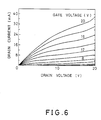
- Fig. 6 is a diagram illustrating drain voltage versus drain current characteristic curves of an N channel type thin film silicon semiconductor device as produced in the above-mentioned manner with the gate voltage as a parameter.
- the channel length and channel width of this thin film silicon semiconductor device were 40 ⁇ m and 1,500 ⁇ m, respectively.
- the carrier mobility found from this figure was 190 cm2/V ⁇ s.
- the thin film silicon semiconductor device according to the present invention shows good triode characteristics and has a large carrier mobility.
- Fig. 7 shows the results of carrier mobilities as measured with respect to samples having a fixed channel width of 10 ⁇ m and varied channel lengths.
- the other production conditions were the same as in the case of the sample as shown in Fig. 4. It can be understood from these results that the variation of carrier mobility was very small even when the channel length was varied. This indicates that, according to the present invention, the lot-to-lot variation of characteristics of thin film silicon semiconductor devices can be very much reduced even if the number of crystal grain boundaries present in the channel varies form lot to lot, thus providing extremely advantageous conditions in actual designing and use of a semiconductor device.
- thin polycrystalline silicon film according to the present invention is a [111] axis-oriented thin polycrystalline silicon film comprising the largest number of crystal grains having a [111] axis in the direction perpendicular to the surface of a substrate or in a direction close thereto and a small number of crystal grains having a 220 axis or a [311] axis in those directions.
- the diffraction peak intensity ration (111)/(220) was about 5, which is conspicuously high as against 1.8 as the intensity ratio of a randomly-oriented polycrystalline silicon powder. Further, it was found that the lattice constant determined from the positions of peaks was 5.411 ⁇ , which is smaller than 5.43086 ⁇ (see S.M. Sze: "Physics of Semiconductor Devices", John Wiley & Sons, New York; 1969, P. 58) as the lattice constant of bulk silicon or a thin silicon film formed by a CVD method. The crystal grain size determined from the half value width of the (111) peak was about 0.06 ⁇ m. The thickness of this thin polycrystalline silicon film was 0.16 um.
- Fig. 9 shows the results of examination on the relationships of the carrier mobility (Curve A) and the height of potential barrier determined from the dependence of drain current on temperature (Curve B) with the ratio of the lattice constant a/a0 wherein a represents the lattice constant of polycrystalline silicon film while a0 represents the lattice constant of a silicon single crystal) as regards thin film silicon semiconductor devices. It can be understood from Fig.
- the carrier mobility was as more than 70 cm2/V ⁇ s despite fine crystal grains.
- the ratio of lattice constant was 0.999 or lower, that is, when the ratio of the lattice constant of the thin polycrystalline silicon film to that of the silicon single crystal is 0.999 or less, the carrier mobility was 150 cm2/V ⁇ s or higher.
- a thin polycrystalline silicon film having a lattice constant equal to or larger than that of the silicon single crystal is used, no thin film silicon semiconductor device having excellent characteristics can be obtained.
- the thin film silicon semiconductor device of the present invention has excellent characteristics despite a minute crystal grain size, as compared with the conventional ones.
- the fact that excellent characteristics can be secured despite a minute crystal grain size is of great significance in producing thin film silicon semiconductor devices in high yield.
- Crystal grain boundaries are conspicuously different in not only electrical properties but also processability from the insides of crystal grains. Therefore, crystal grain boundaries are notably corroded in processing a thin silicon film by a wet or dry etching process, as compared with the insides of crystal grains. This results in a difficulty in sharply processing the sides of the pattern of a thin silicon film comprising large crystal grains shown in Fig. 3 in the case of a conventional thin film silicon semiconductor device.
- a thin silicon film can be sharply processed by virtue of minute crystal grains constituting the same to enable a fine semiconductor device to be easily produced.
- a thin polycrystalline silicon film for realize a thin film semiconductor device having excellent performance characteristics is obtained when high energy particles collides with silicon atoms already deposited on a substrate during the course of deposition of a thin silicon film to push some silicon atoms into the inside of the film. Therefore, it is believed that the properties of the deposited thin film differ due to sputtering conditions.
- a film of the kind as described above can also be obtained by a vacuum evaporation and deposition method combined with irradiation of a film being deposited with high energy particles during the process of formation of the film, which method, however, requires a unit for emission and acceleration of high energy particles in addition to an evaporation source, leading to a difficulty in deposition on a large-sized substrate and in uniform deposition.
- Such problems can be easily solved by the sputtering method.
- Fig. 10 shows variations of the carrier mobility (Curve C) and the height of potential barrier developed in crystal grain boundaries (Curve D) with the sputtering gas pressure at the time of deposition of thin silicon film.
- Argon was used as a sputtering gas for deposition of a thin silicon film, while a laser annealing method was employed for polycrystallization under annealing conditions involving a laser power of 2.8 W and an irradiation time of 1 ms.
- the deposited thin silicon films showed 111 axis orientation irrespective of the argon pressure.
- the lower the sputtering gas pressure the lower the potential barrier and hence the higher the carrier mobility.
- the effect was notable.
- the pressure was 2.5 Pa or lower
- the carrier mobility becomes 150 cm2/V ⁇ s.
- the frequnency of collision of high energy particles with argon atoms increases to lose the energy of high energy particles colliding with a substrate, resulting in a reduction in the aforementioned knock-on effect. Therefore, as shown in Fig. 10, the carrier mobility notably lowered when the sputtering gas pressure exceeded 3.5 Pa.
- a thin polycrystalline silicon film and the characteristics of a thin film silicon semiconductor device vary depending on annealing conditions for polycrystallization.
- Thin amorphous silicon films deposited by sputtering under an argon gas pressure of 2.0 Pa were polycrystallized by irradiation with respective argon laser beams with varied irradiation outputs, followed by the procedure of the process as shown in Figs. 4A-4D to produce thin film silicon semiconductor devices.
- Fig. 11 shows a relationship between the carrier mobility and the irradiation output of laser beam as regards the semiconductor devices thus produced.
- the irradiation time was one millisecond in every case. It can be understood from these results that the carrier mobility notably increases with an increase in the output of laser beam.
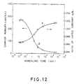
- Thin amorphous silicon films deposited by sputtering at an argon gas pressure of 2.0 Pa were respectively irradiated with an argon laser beam for varied irradiation times to effect polycrystallization thereof, followed by the procedure of the process as shown in Figs. 4A-4D to produce thin film silicon semiconductor devices.
- Fig. 12 shows variations of the carrier mobility (Curve E) and the rate of change in the lattice constant of thin polycrystalline silicon film (Curve F) with the annealing time.
- a laser beam irradiation method was employed.
- an infrared ray irradiation method was employed.
- annealing was conducted in an electric furnace. The laser beam irradiation was conducted by scanning a laser beam having a diameter of 50 ⁇ m at an irradiation output of 2.8 W.
- the whole surface of a thin silicon film was irradiated with infrared rays to keep the surface temperature of the thin film at 1,200° C.
- the temperature of the electric furnace was kept at 1,100°C.
- Annealing for up to 10 seconds gave thin polycrystalline silicon films having a lattice constant smaller than that of a silicon single crystal and thin film silicon semiconductor devices having a high carrier mobility.
- the carrier mobility decreased.
- a thin polycrystalline silicon film according to the present invention has a lattice constant smaller than that of a silicon single crystal, and conditions for obtaining such a thin polycrystalline silicon film involve a pressure of 3.5 Pa or lower at the time of sputtering and an annealing time of 10 seconds or shorter for polycrystallization.
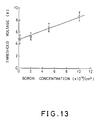
- Fig. 13 is a diagram illustrating relationship between the boron (B) concentration of thin silicon film and the gate voltage for initiating operation of a semiconductor device comprising the thin silicon film, namely the threshold voltage.
- B boron
- the boron concentration is a value calculated from the amount of ion implantation and the thickness of the silicon film. It can be understood from the results shown in this figure that the threshold voltage increases with an increase in the boron concentration, thus indicating that the threshold voltage can be controlled by the boron concentration.
- the resulting thin silicon film acts as a high concentration impurity-doped resistor incapable of allowing a sufficiently high on-off current ratio to be secure, leading to a difficulty in operating a semiconductor device comprising the same as such.
- a method in which sputtering is effected using a sputtering target as shown in Fig. 5 which contains a predetermined amount of boron, that is 1014 - 1017/cm3, preliminarily added thereto may also be employed as the method of introducing boron into a thin silicon film.
- this method enables introduction of boron to be effected uniformly along the thickness-wise direction of a thin silicon film simultaneously with the formation of the thin silicon film only by preliminary addition of a predetermined amount of boron to a target, thus advantageously leading to a reduction in the number of production steps.
- the thickness of a thin silicon film for effectively embodying the present invention is most suitably in a range of 0.01 to 2.0 ⁇ m. When it is smaller than 0.01 ⁇ m, uniform annealing is difficult. When it exceeds 20 ⁇ m, patterning of a thin silicon film by etching is so difficult that a semiconductor device having a thin structure cannot be produced.
- argon was used as the sputtering gas in the foregoing examples, other inert gas such as helium, neon, xenon or krypton, or a mixture of various inert gases may be used to obtain the same thin amorphous silicon film as obtained using argon for producing a thin film silicon semiconductor device having excellent characteristics.
- the laser beam irradiation method was employed as the short-time annealing method for effecting crystallization of a thin amorphous silicon film in the foregoing examples, other method including an electron beam irradiation method and an infrared ray irradiation method can be employed.
- the electron beam irradiation method is suitable for production of a semiconductor device and a three-dimensional integrated circuit on a glass substrate since it enables selective annealing to be effected only on and around a thin silicon film while keeping a substrate at a low temperature.
- the infrared ray irradiation method which uses light emitted from a halogen lamp or the like, is advantageous in that a thin silicon film can be annealed as a whole all at once.
- a thin silicon film formed by sputter deposition can easily effect polycrystallizaiton of the thin silicon film to enable a thin film silicon semiconductor device having sufficiently excellent characteristics to be produces as in the case of the laser beam irradiation method.
- the annealing time for polycrystallization exceeds 10 seconds, in the case of the infrared ray irradiation method for example, however, not only a thin silicon film but also a substrate is heated, and, in the case of a three-dimensional integrated circuit, the lower-layer semiconductor device thereof is deteriorated or broken.
- the annealing time must be 10 seconds or shorter.
- the present invention can also be applied to both an N channel type and a P channel type thin film silicon semiconductor devices.
- the two types of thin film silicon semiconductor devices as shown in Figs. 1 and 2 respectively include an N channel type using electrons as carriers and a P channel type using holes as carriers like a single crystal bulk semiconductor device, and the former can be produced by adding phosphorus or arsenic capable of acting as an N-type impurity to silicon in source electrode/drain electrode while the latter can be produced by adding boron capable of acting as a P-type impurity to silicon in source electrode/drain electrode.
- the effective concentration of phosphorus and arsenic is equal to that of boron and within the range from 1014/cm3 to 1017/cm3.
- Phosphorus and arsenic can be introduced by sputter deposition.
- the present invention can also be applied to the stagger structure. Specifically, a gate electrode is first formed, a gate insulating film is then deposited, and thereafter a thin silicon film is formed, followed by short-time annealing.
- a thin film silicon semiconductor device having a stagger structure can be produced only by changing part of the order of the steps involved in the production of a thin film silicon semiconductor device having a coplanar structure. It will be apparent that this provides a thin film silicon semiconductor device having excellent characteristics.
- the present invention provides an advantage that high-performance thin film silicon semiconductor devices can produced at low cost and in high yield.
Landscapes
- Recrystallisation Techniques (AREA)
- Thin Film Transistor (AREA)
- Physical Deposition Of Substances That Are Components Of Semiconductor Devices (AREA)
Applications Claiming Priority (4)
| Application Number | Priority Date | Filing Date | Title |
|---|---|---|---|
| JP185361/87 | 1987-07-27 | ||
| JP18536187 | 1987-07-27 | ||
| JP167841/88 | 1988-07-07 | ||
| JP63167841A JPH07114184B2 (ja) | 1987-07-27 | 1988-07-07 | 薄膜形シリコン半導体装置およびその製造方法 |
Publications (3)
| Publication Number | Publication Date |
|---|---|
| EP0301463A2 true EP0301463A2 (fr) | 1989-02-01 |
| EP0301463A3 EP0301463A3 (fr) | 1989-09-20 |
| EP0301463B1 EP0301463B1 (fr) | 1997-01-22 |
Family
ID=26491765
Family Applications (1)
| Application Number | Title | Priority Date | Filing Date |
|---|---|---|---|
| EP88111984A Expired - Lifetime EP0301463B1 (fr) | 1987-07-27 | 1988-07-25 | Dispositif semi-conducteur à film mince en silicium et procédé pour le fabriquer |
Country Status (4)
| Country | Link |
|---|---|
| US (1) | US5132754A (fr) |
| EP (1) | EP0301463B1 (fr) |
| JP (1) | JPH07114184B2 (fr) |
| DE (1) | DE3855765T2 (fr) |
Cited By (9)
| Publication number | Priority date | Publication date | Assignee | Title |
|---|---|---|---|---|
| US5114869A (en) * | 1988-05-30 | 1992-05-19 | Seikosha Co., Ltd. | Method for producing reverse staggered type silicon thin film transistor |
| EP0502749A3 (en) * | 1991-03-06 | 1993-05-19 | Semiconductor Energy Laboratory Co., Ltd. | Gate structure of field effect device and method for forming the same |
| EP0459836B1 (fr) * | 1990-06-01 | 1997-09-17 | Sel Semiconductor Energy Laboratory Co., Ltd. | Procédé pour fabriquer des transistors à film mince |
| US6136625A (en) * | 1991-05-08 | 2000-10-24 | Seiko Epson Corporation | Method of manufacturing an active matrix panel |
| EP0984317A3 (fr) * | 1993-12-02 | 2001-03-21 | Semiconductor Energy Laboratory Co., Ltd. | Dispositif d'affichage à matrice active |
| US6352883B1 (en) | 1991-02-22 | 2002-03-05 | Semiconductor Energy Laboratory Co., Ltd. | Semiconductor device and method for forming the same |
| US6624450B1 (en) | 1992-03-27 | 2003-09-23 | Semiconductor Energy Laboratory Co., Ltd. | Semiconductor device and method for forming the same |
| US6670638B2 (en) * | 2000-09-25 | 2003-12-30 | Hitachi, Ltd. | Liquid crystal display element and method of manufacturing the same |
| US7923356B2 (en) | 2001-06-01 | 2011-04-12 | Semiconductor Energy Laboratory Co., Ltd. | Semiconductor film, semiconductor device and method for manufacturing same |
Families Citing this family (47)
| Publication number | Priority date | Publication date | Assignee | Title |
|---|---|---|---|---|
| US5753542A (en) * | 1985-08-02 | 1998-05-19 | Semiconductor Energy Laboratory Co., Ltd. | Method for crystallizing semiconductor material without exposing it to air |
| US5962869A (en) * | 1988-09-28 | 1999-10-05 | Semiconductor Energy Laboratory Co., Ltd. | Semiconductor material and method for forming the same and thin film transistor |
| US6008078A (en) | 1990-07-24 | 1999-12-28 | Semiconductor Energy Laboratory Co., Ltd. | Method for manufacturing a semiconductor device |
| US5210050A (en) * | 1990-10-15 | 1993-05-11 | Semiconductor Energy Laboratory Co., Ltd. | Method for manufacturing a semiconductor device comprising a semiconductor film |
| TW237562B (fr) | 1990-11-09 | 1995-01-01 | Semiconductor Energy Res Co Ltd | |
| US5849601A (en) | 1990-12-25 | 1998-12-15 | Semiconductor Energy Laboratory Co., Ltd. | Electro-optical device and method for manufacturing the same |
| US7115902B1 (en) | 1990-11-20 | 2006-10-03 | Semiconductor Energy Laboratory Co., Ltd. | Electro-optical device and method for manufacturing the same |
| KR950013784B1 (ko) | 1990-11-20 | 1995-11-16 | 가부시키가이샤 한도오따이 에네루기 겐큐쇼 | 반도체 전계효과 트랜지스터 및 그 제조방법과 박막트랜지스터 |
| US8106867B2 (en) | 1990-11-26 | 2012-01-31 | Semiconductor Energy Laboratory Co., Ltd. | Electro-optical device and driving method for the same |
| KR950001360B1 (ko) * | 1990-11-26 | 1995-02-17 | 가부시키가이샤 한도오따이 에네루기 겐큐쇼 | 전기 광학장치와 그 구동방법 |
| US7154147B1 (en) * | 1990-11-26 | 2006-12-26 | Semiconductor Energy Laboratory Co., Ltd. | Electro-optical device and driving method for the same |
| US7098479B1 (en) | 1990-12-25 | 2006-08-29 | Semiconductor Energy Laboratory Co., Ltd. | Electro-optical device and method for manufacturing the same |
| US7576360B2 (en) * | 1990-12-25 | 2009-08-18 | Semiconductor Energy Laboratory Co., Ltd. | Electro-optical device which comprises thin film transistors and method for manufacturing the same |
| JP3103385B2 (ja) * | 1991-01-25 | 2000-10-30 | 株式会社東芝 | ポリシリコン薄膜半導体装置 |
| EP0499979A3 (en) | 1991-02-16 | 1993-06-09 | Semiconductor Energy Laboratory Co., Ltd. | Electro-optical device |
| JP2873632B2 (ja) | 1991-03-15 | 1999-03-24 | 株式会社半導体エネルギー研究所 | 半導体装置 |
| US6713783B1 (en) | 1991-03-15 | 2004-03-30 | Semiconductor Energy Laboratory Co., Ltd. | Compensating electro-optical device including thin film transistors |
| JP2794499B2 (ja) | 1991-03-26 | 1998-09-03 | 株式会社半導体エネルギー研究所 | 半導体装置の作製方法 |
| JP2845303B2 (ja) | 1991-08-23 | 1999-01-13 | 株式会社 半導体エネルギー研究所 | 半導体装置とその作製方法 |
| US5766344A (en) * | 1991-09-21 | 1998-06-16 | Semiconductor Energy Laboratory Co., Ltd. | Method for forming a semiconductor |
| US6979840B1 (en) * | 1991-09-25 | 2005-12-27 | Semiconductor Energy Laboratory Co., Ltd. | Thin film transistors having anodized metal film between the gate wiring and drain wiring |
| US6964890B1 (en) | 1992-03-17 | 2005-11-15 | Semiconductor Energy Laboratory Co., Ltd. | Semiconductor device and method for forming the same |
| JP2814161B2 (ja) | 1992-04-28 | 1998-10-22 | 株式会社半導体エネルギー研究所 | アクティブマトリクス表示装置およびその駆動方法 |
| US6693681B1 (en) | 1992-04-28 | 2004-02-17 | Semiconductor Energy Laboratory Co., Ltd. | Electro-optical device and method of driving the same |
| JP3065825B2 (ja) * | 1992-10-21 | 2000-07-17 | 株式会社半導体エネルギー研究所 | レーザー処理方法 |
| US7081938B1 (en) | 1993-12-03 | 2006-07-25 | Semiconductor Energy Laboratory Co., Ltd. | Electro-optical device and method for manufacturing the same |
| JPH07176745A (ja) * | 1993-12-17 | 1995-07-14 | Semiconductor Energy Lab Co Ltd | 半導体素子 |
| JP3402400B2 (ja) | 1994-04-22 | 2003-05-06 | 株式会社半導体エネルギー研究所 | 半導体集積回路の作製方法 |
| JP2900229B2 (ja) * | 1994-12-27 | 1999-06-02 | 株式会社半導体エネルギー研究所 | 半導体装置およびその作製方法および電気光学装置 |
| US5834327A (en) * | 1995-03-18 | 1998-11-10 | Semiconductor Energy Laboratory Co., Ltd. | Method for producing display device |
| JP3729955B2 (ja) | 1996-01-19 | 2005-12-21 | 株式会社半導体エネルギー研究所 | 半導体装置の作製方法 |
| US6478263B1 (en) | 1997-01-17 | 2002-11-12 | Semiconductor Energy Laboratory Co., Ltd. | Semiconductor device and its manufacturing method |
| JP3645379B2 (ja) | 1996-01-19 | 2005-05-11 | 株式会社半導体エネルギー研究所 | 半導体装置の作製方法 |
| JP3645380B2 (ja) | 1996-01-19 | 2005-05-11 | 株式会社半導体エネルギー研究所 | 半導体装置の作製方法、情報端末、ヘッドマウントディスプレイ、ナビゲーションシステム、携帯電話、ビデオカメラ、投射型表示装置 |
| JP3645378B2 (ja) * | 1996-01-19 | 2005-05-11 | 株式会社半導体エネルギー研究所 | 半導体装置の作製方法 |
| US7056381B1 (en) | 1996-01-26 | 2006-06-06 | Semiconductor Energy Laboratory Co., Ltd. | Fabrication method of semiconductor device |
| US6180439B1 (en) | 1996-01-26 | 2001-01-30 | Semiconductor Energy Laboratory Co., Ltd. | Method for fabricating a semiconductor device |
| US6100562A (en) | 1996-03-17 | 2000-08-08 | Semiconductor Energy Laboratory Co., Ltd. | Method of manufacturing a semiconductor device |
| US7071041B2 (en) * | 2000-01-20 | 2006-07-04 | Semiconductor Energy Laboratory Co., Ltd. | Method of manufacturing a semiconductor device |
| US7151017B2 (en) * | 2001-01-26 | 2006-12-19 | Semiconductor Energy Laboratory Co., Ltd. | Method of manufacturing semiconductor device |
| JP4718700B2 (ja) | 2001-03-16 | 2011-07-06 | 株式会社半導体エネルギー研究所 | 半導体装置の作製方法 |
| JP4141741B2 (ja) * | 2001-06-01 | 2008-08-27 | 株式会社半導体エネルギー研究所 | 半導体装置の作製方法 |
| US6994083B2 (en) * | 2001-12-21 | 2006-02-07 | Trudell Medical International | Nebulizer apparatus and method |
| JP4326756B2 (ja) * | 2002-07-04 | 2009-09-09 | 株式会社半導体エネルギー研究所 | ドーピング方法、ドーピング装置の制御システム、およびドーピング装置 |
| US7442631B2 (en) * | 2005-02-10 | 2008-10-28 | Semiconductor Energy Laboratory Co., Ltd. | Doping method and method of manufacturing field effect transistor |
| US7791172B2 (en) | 2007-03-19 | 2010-09-07 | Semiconductor Energy Laboratory Co., Ltd. | Nonvolatile semiconductor memory device |
| KR101042636B1 (ko) * | 2008-10-15 | 2011-06-20 | 김용환 | 에너지빔 조사를 이용한 실리콘 박막 제조방법 |
Family Cites Families (11)
| Publication number | Priority date | Publication date | Assignee | Title |
|---|---|---|---|---|
| JPS5662356A (en) * | 1979-10-26 | 1981-05-28 | Seiko Instr & Electronics Ltd | Logic integrated circuit device and its manufacturing method |
| US4363828A (en) * | 1979-12-12 | 1982-12-14 | International Business Machines Corp. | Method for depositing silicon films and related materials by a glow discharge in a disiland or higher order silane gas |
| EP0055032B1 (fr) * | 1980-12-23 | 1986-04-23 | National Research Development Corporation | Transistor à effet de champ |
| JPS5893221A (ja) * | 1981-11-30 | 1983-06-02 | Toshiba Corp | 半導体薄膜構造とその製造方法 |
| JPS58188165A (ja) * | 1982-04-28 | 1983-11-02 | Nec Corp | 半導体装置 |
| US4632712A (en) * | 1983-09-12 | 1986-12-30 | Massachusetts Institute Of Technology | Reducing dislocations in semiconductors utilizing repeated thermal cycling during multistage epitaxial growth |
| JPS60239066A (ja) * | 1984-05-11 | 1985-11-27 | Hitachi Ltd | 半導体装置 |
| US4597160A (en) * | 1985-08-09 | 1986-07-01 | Rca Corporation | Method of fabricating a polysilicon transistor with a high carrier mobility |
| DE3682021D1 (de) * | 1985-10-23 | 1991-11-21 | Hitachi Ltd | Polysilizium-mos-transistor und verfahren zu seiner herstellung. |
| JPS62104173A (ja) * | 1985-10-31 | 1987-05-14 | Fujitsu Ltd | 半導体装置 |
| JPH0793258B2 (ja) * | 1985-12-04 | 1995-10-09 | 富士通株式会社 | 導電体膜の再結晶化方法 |
-
1988
- 1988-07-07 JP JP63167841A patent/JPH07114184B2/ja not_active Expired - Fee Related
- 1988-07-21 US US07/222,966 patent/US5132754A/en not_active Expired - Lifetime
- 1988-07-25 DE DE3855765T patent/DE3855765T2/de not_active Expired - Lifetime
- 1988-07-25 EP EP88111984A patent/EP0301463B1/fr not_active Expired - Lifetime
Cited By (15)
| Publication number | Priority date | Publication date | Assignee | Title |
|---|---|---|---|---|
| US5114869A (en) * | 1988-05-30 | 1992-05-19 | Seikosha Co., Ltd. | Method for producing reverse staggered type silicon thin film transistor |
| US6740547B2 (en) | 1990-06-01 | 2004-05-25 | Semiconductor Energy Laboratory Co., Ltd. | Method for fabricating thin-film transistor |
| EP0459836B1 (fr) * | 1990-06-01 | 1997-09-17 | Sel Semiconductor Energy Laboratory Co., Ltd. | Procédé pour fabriquer des transistors à film mince |
| US6458200B1 (en) | 1990-06-01 | 2002-10-01 | Semiconductor Energy Laboratory Co., Ltd. | Method for fabricating thin-film transistor |
| US7018874B2 (en) | 1990-06-01 | 2006-03-28 | Semiconductor Energy Laboratory Co., Ltd. | Method for fabricating thin-film transistor |
| US6352883B1 (en) | 1991-02-22 | 2002-03-05 | Semiconductor Energy Laboratory Co., Ltd. | Semiconductor device and method for forming the same |
| EP0502749A3 (en) * | 1991-03-06 | 1993-05-19 | Semiconductor Energy Laboratory Co., Ltd. | Gate structure of field effect device and method for forming the same |
| US7569408B1 (en) | 1991-03-06 | 2009-08-04 | Semiconductor Energy Laboratory Co., Ltd. | Semiconductor device and method for forming the same |
| US6323528B1 (en) | 1991-03-06 | 2001-11-27 | Semiconductor Energy Laboratory Co,. Ltd. | Semiconductor device |
| US6822261B2 (en) | 1991-03-06 | 2004-11-23 | Semiconductor Energy Laboratory Co., Ltd. | Semiconductor device and method for forming the same |
| US6136625A (en) * | 1991-05-08 | 2000-10-24 | Seiko Epson Corporation | Method of manufacturing an active matrix panel |
| US6624450B1 (en) | 1992-03-27 | 2003-09-23 | Semiconductor Energy Laboratory Co., Ltd. | Semiconductor device and method for forming the same |
| EP0984317A3 (fr) * | 1993-12-02 | 2001-03-21 | Semiconductor Energy Laboratory Co., Ltd. | Dispositif d'affichage à matrice active |
| US6670638B2 (en) * | 2000-09-25 | 2003-12-30 | Hitachi, Ltd. | Liquid crystal display element and method of manufacturing the same |
| US7923356B2 (en) | 2001-06-01 | 2011-04-12 | Semiconductor Energy Laboratory Co., Ltd. | Semiconductor film, semiconductor device and method for manufacturing same |
Also Published As
| Publication number | Publication date |
|---|---|
| DE3855765D1 (de) | 1997-03-06 |
| DE3855765T2 (de) | 1997-08-14 |
| US5132754A (en) | 1992-07-21 |
| JPH07114184B2 (ja) | 1995-12-06 |
| EP0301463A3 (fr) | 1989-09-20 |
| EP0301463B1 (fr) | 1997-01-22 |
| JPH01103825A (ja) | 1989-04-20 |
Similar Documents
| Publication | Publication Date | Title |
|---|---|---|
| EP0301463A2 (fr) | Dispositif semi-conducteur à film mince en silicium et procédé pour le fabriquer | |
| US5248630A (en) | Thin film silicon semiconductor device and process for producing thereof | |
| Kakkad et al. | Crystallized Si films by low‐temperature rapid thermal annealing of amorphous silicon | |
| US6271066B1 (en) | Semiconductor material and method for forming the same and thin film transistor | |
| US7169657B2 (en) | Process for laser processing and apparatus for use in the same | |
| US5965904A (en) | Semiconductor device comprising silicon semiconductor layer | |
| JPH04100233A (ja) | 半導体装置の製造方法 | |
| US6562672B2 (en) | Semiconductor material and method for forming the same and thin film transistor | |
| KR960008499B1 (ko) | 레이저 처리방법 및 레이저 처리장치 | |
| US5252498A (en) | Method of forming electronic devices utilizing diamond | |
| EP0684632B1 (fr) | Procédé de fabrication d'un film à basse température pour un dispositif semi-conducteur | |
| JP2840802B2 (ja) | 半導体材料の製造方法および製造装置 | |
| JP4036278B2 (ja) | イオンドーピング装置 | |
| JP3119988B2 (ja) | 半導体装置の作製方法 | |
| JP3065528B2 (ja) | 半導体装置 | |
| JP3051363B2 (ja) | 半導体装置の作製方法 | |
| JPS60241268A (ja) | 薄膜トランジスタの製造方法 | |
| JP3564505B2 (ja) | 半導体装置の作製方法 | |
| JP3340407B2 (ja) | 絶縁被膜および半導体装置 | |
| JP3241705B2 (ja) | 薄膜トランジスタの作製方法 | |
| JP3160269B2 (ja) | 半導体装置の作製方法 | |
| JP3397760B2 (ja) | 薄膜トランジスタの作製方法 | |
| JP3340425B2 (ja) | 半導体装置の作製方法 | |
| JP3120079B2 (ja) | 絶縁被膜および半導体装置 | |
| JP3340429B2 (ja) | 半導体装置 |
Legal Events
| Date | Code | Title | Description |
|---|---|---|---|
| PUAI | Public reference made under article 153(3) epc to a published international application that has entered the european phase |
Free format text: ORIGINAL CODE: 0009012 |
|
| 17P | Request for examination filed |
Effective date: 19880725 |
|
| AK | Designated contracting states |
Kind code of ref document: A2 Designated state(s): DE FR GB |
|
| PUAL | Search report despatched |
Free format text: ORIGINAL CODE: 0009013 |
|
| RHK1 | Main classification (correction) |
Ipc: H01L 21/20 |
|
| AK | Designated contracting states |
Kind code of ref document: A3 Designated state(s): DE FR GB |
|
| 17Q | First examination report despatched |
Effective date: 19920702 |
|
| RAP1 | Party data changed (applicant data changed or rights of an application transferred) |
Owner name: NIPPON TELEGRAPH AND TELEPHONE CORPORATION |
|
| GRAG | Despatch of communication of intention to grant |
Free format text: ORIGINAL CODE: EPIDOS AGRA |
|
| GRAH | Despatch of communication of intention to grant a patent |
Free format text: ORIGINAL CODE: EPIDOS IGRA |
|
| GRAH | Despatch of communication of intention to grant a patent |
Free format text: ORIGINAL CODE: EPIDOS IGRA |
|
| GRAA | (expected) grant |
Free format text: ORIGINAL CODE: 0009210 |
|
| AK | Designated contracting states |
Kind code of ref document: B1 Designated state(s): DE FR GB |
|
| REF | Corresponds to: |
Ref document number: 3855765 Country of ref document: DE Date of ref document: 19970306 |
|
| ET | Fr: translation filed | ||
| PLBE | No opposition filed within time limit |
Free format text: ORIGINAL CODE: 0009261 |
|
| STAA | Information on the status of an ep patent application or granted ep patent |
Free format text: STATUS: NO OPPOSITION FILED WITHIN TIME LIMIT |
|
| 26N | No opposition filed | ||
| REG | Reference to a national code |
Ref country code: GB Ref legal event code: IF02 |
|
| PGFP | Annual fee paid to national office [announced via postgrant information from national office to epo] |
Ref country code: DE Payment date: 20070731 Year of fee payment: 20 |
|
| PGFP | Annual fee paid to national office [announced via postgrant information from national office to epo] |
Ref country code: GB Payment date: 20070725 Year of fee payment: 20 |
|
| PGFP | Annual fee paid to national office [announced via postgrant information from national office to epo] |
Ref country code: FR Payment date: 20070710 Year of fee payment: 20 |
|
| REG | Reference to a national code |
Ref country code: GB Ref legal event code: PE20 Expiry date: 20080724 |
|
| PG25 | Lapsed in a contracting state [announced via postgrant information from national office to epo] |
Ref country code: GB Free format text: LAPSE BECAUSE OF EXPIRATION OF PROTECTION Effective date: 20080724 |