EP0301869A1 - Dispositif d'affichage à cristal liquide - Google Patents
Dispositif d'affichage à cristal liquide Download PDFInfo
- Publication number
- EP0301869A1 EP0301869A1 EP88306976A EP88306976A EP0301869A1 EP 0301869 A1 EP0301869 A1 EP 0301869A1 EP 88306976 A EP88306976 A EP 88306976A EP 88306976 A EP88306976 A EP 88306976A EP 0301869 A1 EP0301869 A1 EP 0301869A1
- Authority
- EP
- European Patent Office
- Prior art keywords
- liquid crystal
- display device
- transparent
- crystal display
- transparent conductive
- Prior art date
- Legal status (The legal status is an assumption and is not a legal conclusion. Google has not performed a legal analysis and makes no representation as to the accuracy of the status listed.)
- Granted
Links
- 239000004973 liquid crystal related substance Substances 0.000 title claims abstract description 61
- 239000000758 substrate Substances 0.000 claims abstract description 55
- 238000002834 transmittance Methods 0.000 claims description 5
- 239000011347 resin Substances 0.000 claims description 4
- 229920005989 resin Polymers 0.000 claims description 4
- 239000000463 material Substances 0.000 claims description 3
- 230000003287 optical effect Effects 0.000 claims description 3
- 238000000034 method Methods 0.000 description 12
- 239000002184 metal Substances 0.000 description 7
- 229920002120 photoresistant polymer Polymers 0.000 description 5
- 238000010276 construction Methods 0.000 description 4
- 238000004070 electrodeposition Methods 0.000 description 4
- 238000004519 manufacturing process Methods 0.000 description 4
- 238000003475 lamination Methods 0.000 description 3
- 229920006254 polymer film Polymers 0.000 description 3
- 230000001603 reducing effect Effects 0.000 description 3
- 230000008859 change Effects 0.000 description 2
- 238000001704 evaporation Methods 0.000 description 2
- 238000001755 magnetron sputter deposition Methods 0.000 description 2
- 230000004048 modification Effects 0.000 description 2
- 238000012986 modification Methods 0.000 description 2
- 125000006850 spacer group Chemical group 0.000 description 2
- 108010010803 Gelatin Proteins 0.000 description 1
- 230000000740 bleeding effect Effects 0.000 description 1
- 239000001055 blue pigment Substances 0.000 description 1
- 239000005018 casein Substances 0.000 description 1
- BECPQYXYKAMYBN-UHFFFAOYSA-N casein, tech. Chemical compound NCCCCC(C(O)=O)N=C(O)C(CC(O)=O)N=C(O)C(CCC(O)=N)N=C(O)C(CC(C)C)N=C(O)C(CCC(O)=O)N=C(O)C(CC(O)=O)N=C(O)C(CCC(O)=O)N=C(O)C(C(C)O)N=C(O)C(CCC(O)=N)N=C(O)C(CCC(O)=N)N=C(O)C(CCC(O)=N)N=C(O)C(CCC(O)=O)N=C(O)C(CCC(O)=O)N=C(O)C(COP(O)(O)=O)N=C(O)C(CCC(O)=N)N=C(O)C(N)CC1=CC=CC=C1 BECPQYXYKAMYBN-UHFFFAOYSA-N 0.000 description 1
- 235000021240 caseins Nutrition 0.000 description 1
- 238000004132 cross linking Methods 0.000 description 1
- 230000003247 decreasing effect Effects 0.000 description 1
- 238000004043 dyeing Methods 0.000 description 1
- 230000008020 evaporation Effects 0.000 description 1
- 229920000159 gelatin Polymers 0.000 description 1
- 239000008273 gelatin Substances 0.000 description 1
- 235000019322 gelatine Nutrition 0.000 description 1
- 235000011852 gelatine desserts Nutrition 0.000 description 1
- 239000003292 glue Substances 0.000 description 1
- 239000001056 green pigment Substances 0.000 description 1
- AMGQUBHHOARCQH-UHFFFAOYSA-N indium;oxotin Chemical compound [In].[Sn]=O AMGQUBHHOARCQH-UHFFFAOYSA-N 0.000 description 1
- 239000011810 insulating material Substances 0.000 description 1
- 239000011159 matrix material Substances 0.000 description 1
- 239000012860 organic pigment Substances 0.000 description 1
- 239000000049 pigment Substances 0.000 description 1
- 229920000642 polymer Polymers 0.000 description 1
- 230000008569 process Effects 0.000 description 1
- 239000001054 red pigment Substances 0.000 description 1
- 230000004044 response Effects 0.000 description 1
- 238000007650 screen-printing Methods 0.000 description 1
- 239000002904 solvent Substances 0.000 description 1
- 239000000126 substance Substances 0.000 description 1
- 230000000007 visual effect Effects 0.000 description 1
- 229920003169 water-soluble polymer Polymers 0.000 description 1
Images



Classifications
-
- G—PHYSICS
- G02—OPTICS
- G02F—OPTICAL DEVICES OR ARRANGEMENTS FOR THE CONTROL OF LIGHT BY MODIFICATION OF THE OPTICAL PROPERTIES OF THE MEDIA OF THE ELEMENTS INVOLVED THEREIN; NON-LINEAR OPTICS; FREQUENCY-CHANGING OF LIGHT; OPTICAL LOGIC ELEMENTS; OPTICAL ANALOGUE/DIGITAL CONVERTERS
- G02F1/00—Devices or arrangements for the control of the intensity, colour, phase, polarisation or direction of light arriving from an independent light source, e.g. switching, gating or modulating; Non-linear optics
- G02F1/01—Devices or arrangements for the control of the intensity, colour, phase, polarisation or direction of light arriving from an independent light source, e.g. switching, gating or modulating; Non-linear optics for the control of the intensity, phase, polarisation or colour
- G02F1/13—Devices or arrangements for the control of the intensity, colour, phase, polarisation or direction of light arriving from an independent light source, e.g. switching, gating or modulating; Non-linear optics for the control of the intensity, phase, polarisation or colour based on liquid crystals, e.g. single liquid crystal display cells
- G02F1/133—Constructional arrangements; Operation of liquid crystal cells; Circuit arrangements
- G02F1/1333—Constructional arrangements; Manufacturing methods
- G02F1/1335—Structural association of cells with optical devices, e.g. polarisers or reflectors
- G02F1/133509—Filters, e.g. light shielding masks
- G02F1/133514—Colour filters
Definitions
- This invention relates to a liquid crystal display device suitable for use in a color display such as a color television set.
- a liquid crystal color display device has the following construction.
- a plurality of transparent electrodes are formed on each of two transparent substrates and a color filter is provided over the transparent electrodes on either of the two transparent substrates.
- the two transparent substrates are faced to each other with the electrodes-formed sides inside.
- An orientational film is formed for orientation, covering the entire surface of that side of each transparent substrate facing the other transparent substrate.
- TN (Twisted Nematic) liquid crystal is filled in the space between the orientational films.
- a deflecting plate is provided on the other side of each transparent substrate.
- the color filter is normally positioned as close to the liquid crystal layer as possible.
- Liquid crystal color display devices are divided into two types according to the position of the color filter: the one with a color filter provided over the transparent electrodes formed on a transparent substrate, and the one with a color filter provided on a transparent substrate and with transparent electrodes formed over the color filter.
- a plurality of X-electrodes are formed on one of two transparent substrates and a plurality of Y-electrodes on the other transparent substrate, the X-electrodes and Y-electrodes being arranged in the crossing directions and being made to face each other to form display picture elements at the intersections.
- the liquid crystal display device of this type is driven in so-called a time division drive method, that is, by scanning the X-electrodes sequentially and applying display or non-display voltage to the Y-electrodes corresponding to the picture elements on the selected X-electrodes.
- Liquid crystal is relatively slow in response, and has a property that the light transmittance becomes constant after being scanned repeatedly.
- a liquid crystal display device of a high duty ratio which is expected to provide a wider visual angle and a higher contrast, however, it is desirable that the light transmittance of the liquid crystal changes sharply when applied voltage reaches a specified threshold value.
- liquid crystal color display device with the color filter formed over the transparent electrodes
- applied voltage is reduced by the color filter, causing slower change in the light transmittance around the threshold value of applied voltage.
- the liquid crystal color display device with the transparent electrodes formed over the color filter is more preferable.
- the display device of this type because of the thermal resistance limitation of the color filter, it is not allowed to raise the substrate temperature high enough to form transparent electrodes of a small resistance which is essential to a liquid crystal display device of a high duty ratio.
- a liquid crystal display device has been proposed in which the resistance of the transparent electrodes is lowered by forming metal electrodes on the transparent electrodes.
- Fig. 5 is a plan view of a transparent substrate 4 with a color filter 1, transparent electrodes 2 and metal electrodes 3 formed thereon, for use in a typical liquid crystal display device by the conventional art.
- Fig. 6 is a sectional view of the transparent substrate 4 cut along the line VI-VI of Fig. 5.
- transparent electrodes 5 formed on another transparent substrate to be arranged as opposed to the transparent substrate 4 are shown by broken lines.
- the color filter 1 is formed into a pattern of, say, a red color filter 1R, a green color filter 1G, a blue color filter 1B, a red color filter 1R, and so on.
- the transparent electrodes 2 distinguished by vertical lines look red, those distinguished by oblique lines look green, and those distinguished by horizontal lines look blue.
- the electrode for applying voltage to the liquid crystal layer is made up of the combination of a transparent electrode 2 and a metal electrode 3.
- the portion of the transparent electrode 2 on which the metal electrode 3 is placed shields light, resulting in reduced aperture of the picture elements realized by the combination between the transparent electrodes 2 and transparent electrodes 5. This hampers presentation of a clear picture.
- Another object of the present invention is to provide a liquid crystal display device capable of showing a clear color picture of a high contrast without reducing the aperture of each picture element, thus providing a display of good quality.
- a liquid crystal display device including a pair of transparent substrates and liquid crystal filled in the space between the transparent substrates comprises first transparent conductive films formed selectively on at least one of the transparent substrates, colored transmitting members formed on the first transparent conductive films, and second transparent conductive films covering the colored transmitting members and connected with the first transparent conductive films in the regions where the colored transmitting members are not formed.
- the first transparent conductive films are formed on at least one of the transparent substrates, and the colored transmitting members on the first transparent conductive films.
- the second transparent conductive films are formed over the colored transmitting members so that the second transparent conductive films are in contact with the first transparent conductive films in the areas where no colored transmitting members are formed.
- the first transparent conductive films provide sufficiently high conductivity, having the same function as the metal electrodes of the conventional art. Consequently, the present invention realizes a liquid crystal display device which eliminates the conventional display disadvantages caused by colored transmitting members without reducing the aperture of the colored transmitting members.
- Fig. 1 is a sectional view showing the construction of an embodiment of the liquid crystal display device 11 of the present invention.
- the liquid crystal display device 11 of the present invention is driven by the simple matrix method for color display, although the invention is applicable to liquid crystal color display devices driven by other methods.
- ITO (Indium-Tin-Oxide) films 13 are formed in a stripe pattern as first transparent conducivelytive films on the side of a transparent substrate 12 facing a liquid crystal layer.
- Color filters 14 are formed into a specified pattern as colored transmitting members on the ITO films 13.
- Each of the color filters 14 on the ITO films 13 is red, green or blue.
- red filters are referred to by color filters 14R, green filters by color filters 14G, and blue filters by color filters 14B.
- ITO films 15 are formed as second transparent conducivelytive films over the color filters 14 on the ITO films 13 so that the ITO films 15 are made in contact with the ITO films 13 between the color filters 14.
- the ITO films 13 and 15 constitute bar-shaped transparent electrodes 30.
- a black mask 16 is formed on the portions around the color filters 14 on the ITO films 15 as well as on the portions where the transparent electrodes 30 are not formed.
- An orientational film 17 is formed, covering the entire surface facing the liquid crystal layer.
- a deflecting plate 18 is provided on the surface of the transparent substrate 12 opposite from the lamination.
- a transparent substrate 19 is arranged as opposed to the transparent substrate 12.
- ITO films 20 of a stripe pattern in the direction at a right angle to the direction of the transparent electrodes 30.
- An orientational film 21 is formed to cover the transparent substrate 19 as well as the ITO films 20 formed thereon.
- a deflecting plate 22 is provided on the surface of the transparent substrate 19 opposite from the lamination.
- the transparent substrate 12 and the transparent substrate 19 are spaced apart from each other by a spacer 23, and the space is filled up with liquid crystal 24 of, say TN (twisted nematic) type.
- Fig. 2 is a plan view of the transparent substrate 12 on which the ITO films 13, the color filters 14, the ITO films 15 and the light shielding black mask 16 are formed.
- the black mask 16 is distinguished by right-up oblique lines.
- the filter portions with vertical lines (14R) should look red
- the portions with right-down oblique lines (14G) should look green
- the portions with horizontal lines (14B) should look blue.
- ITO films 15R the films on which red color filters 14R are formed and therefore constitute red-looking transparent electrodes 30
- ITO films 15G and 15B are referred to by ITO films 15G and 15B, respectively.
- the transparent electrodes 30 are formed in different lengths depending upon the color of the color filters 14 to be formed thereon, so that a color filter 14 of correct color is formed on a correct position.
- the ITO film 13 on which the color filters 14R are formed are referred to by ITO films 13R
- those with the color filters 14G formed thereon are referred to by ITO films 13G
- those with the color filters 14B formed thereon by ITO films 13B are referred to by ITO films 13B.
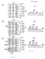
- Figs. 3(1) through 3(7) are plan views showing the manufacturing steps of the liquid crystal display device 11.
- Figs. 4(1) through 4(7) are sectional views for explaining the manufacturing steps corresponding to those shown in Figs. 3(1) through 3(7). The manufacturing process of the liquid crystal display device 11 is described in the following with reference to these figures.
- ITO film 13 is formed by the magnetron sputtering technique on a transparent substrate 12 which is heated up to 300 to 350°C.
- the ITO film 13 thus formed shows sufficiently high conductivity.
- the ITO film 13 is etched into a pattern of stripes of different lengths. That is, an ITO film 13R on which a red color filter 14R is to be formed, an ITO film 13G on which a green color filter 14G is to be formed and an ITO film 13B on which a blue color filter 14B is to be formed have different lengths to be distinguishable from one another.
- Photo resists 25 are formed into a specified pattern to cross the ITO films 13.
- red color filters 14R are formed on the ITO film 13R by the electrodeposition method in the following procedure.
- Electrodeposition solution is prepared by making polymer substance with electrical polarity and red pigment dispersed uniformly in solvent.
- the transparent substrate 12 with the ITO films 13 and the photo resists 25 formed thereon as shown in Figs. 3(1) and 4(1) is dipped as an electrode in the electrodeposition solution.
- the opposite electrode is also dipped in the solution.
- red polymer film is deposited on the ITO film 13R (Since the photo resists 25 are made of insulating material, polymer film is not formed on the photo resists 25).
- the polymer film is heated, cross-linking reaction occurs, forming firm and stable color filters 14R as shown in Figs. 3(2) and 4(2).
- Fig. 4(2) shows the section of the part related to the ITO film 13R of Fig. 3(2).
- ITO film 15 is then formed by the magnetron sputtering technique while the transparent substrate 12 is kept at a temperature not higher than 200°C.
- the ITO film 15 is patterned into ITO films 15R, 15G and 15B corresponding to the ITO films 13R, 13G and 13B as shown in Figs. 3(5) and 4(5).
- the substrate temperature must be kept at 200°C or lower because of the heat resistance limitation of the color filters 14. If the substrate 12 were heated higher than 200°C, the color filters 14 would be discolored.
- UV-setting resin 16a containing black pigment is applied as shown in Figs. 3(6) and 4(6), and ultraviolet ray is radiated in the direction indicated by the arrow R1 on the substrate 12 as shown in Fig. 4(6). Since the color filters 14 do not transmit ultraviolet ray, only the portion of the UV-setting resin 16a where there are no color filters 14 is hardened. When the part of the UV-setting resin 16a which is not hardened is removed, a black mask 16 as shown in Figs. 3(7) and 4(7) is obtained. The structure shown in Fig. 2 is thus manufactured.
- An orientational film 17 is then formed to cover the entire surface facing the liquid crystal ray, and a deflecting plate 18 is provided on the other surface of the transparent substrate 12 opposite from the liquid crystal ray.
- a transparent substrate 19 is placed opposite to the transparent substrate 12, and ITO films 20 are formed in a stripe pattern on the surface of the transparent substrate 19 facing the liquid crystal lay.
- the ITO films 20 on the transparent substrate 19 and the transparent electrodes 30 on the transparent substrate 12 face and cross each other.
- An orientational film 21 is then formed to cover the transparent substrate 19 and the ITO films 20 formed thereon, and a deflecting plate 22 is provided on the other surface of the transparent substrate 19 opposite from the lamination.
- a spacer 23 is placed between the transparent substrate 12 and the transparent substrate 19 to space them apart.
- Liquid crystal 24 is put in to fill up the space between the orientational films 17 and 21.
- the liquid crystal display device 11 shown in Fig. 1 is obtained.
- the transparent electrodes 30 of the liquid crystal display device 11 comprise ITO films 13 which provide sufficiently high conductivity and ITO films 15 which cover the color filters 14 and are made in contact with the ITO films 13 between the color filters 14, the ITO films 13 having the same function as the metal electrodes 3 of the conventional art. Consequently, the resistance of the transparent electrodes 30 can be reduced as desired without decreasing the aperture of the color filters 14.
- the liquid crystal display device 11 of the present invention changes its light transmittance sharply around a threshold voltage value at which the optical characteristic of the liquid crystal 24 changes, and therefore presents a color picture of high quality even if the number of transparent electrodes is increased for higher time-division drive.
- the black mask 16 makes the picture clearer.
- the electrodeposition method is used for forming color filters.
- Other methods as follows may be used.
- the first one is a screen-printing method in which color filters are printed using colored ink (as disclosed in the Japanese Patent Laid-Open Publication No. 58-46326).
- the second one is a dyeing method in which water-soluble polymer film of photosensitive gelatin, glue or casein is formed into a pattern and dyed selectively to make a specified pattern by the photo process (as disclosed in Uchida, JAPAN DISPLAY '83, P. 202 to 205).
- the third one is an evaporation method in which organic pigment is deposited by evaporation to form a specified pattern (as disclosed in Sugata, et al, JAPAN DISPLAY '83, P. 210 to 212).
- the present invention realizes a liquid crystal display device which is capable of providing a color picture of an optimum contrast with no color bleeding without reducing the aperture of the colored light transmitting member.
Landscapes
- Physics & Mathematics (AREA)
- Nonlinear Science (AREA)
- Mathematical Physics (AREA)
- Chemical & Material Sciences (AREA)
- Crystallography & Structural Chemistry (AREA)
- General Physics & Mathematics (AREA)
- Optics & Photonics (AREA)
- Liquid Crystal (AREA)
- Optical Filters (AREA)
- Devices For Indicating Variable Information By Combining Individual Elements (AREA)
Applications Claiming Priority (2)
| Application Number | Priority Date | Filing Date | Title |
|---|---|---|---|
| JP62188264A JPS6432233A (en) | 1987-07-28 | 1987-07-28 | Liquid crystal display device |
| JP188264/87 | 1987-07-28 |
Publications (2)
| Publication Number | Publication Date |
|---|---|
| EP0301869A1 true EP0301869A1 (fr) | 1989-02-01 |
| EP0301869B1 EP0301869B1 (fr) | 1992-09-09 |
Family
ID=16220630
Family Applications (1)
| Application Number | Title | Priority Date | Filing Date |
|---|---|---|---|
| EP88306976A Expired - Lifetime EP0301869B1 (fr) | 1987-07-28 | 1988-07-28 | Dispositif d'affichage à cristal liquide |
Country Status (4)
| Country | Link |
|---|---|
| US (1) | US4935757A (fr) |
| EP (1) | EP0301869B1 (fr) |
| JP (1) | JPS6432233A (fr) |
| DE (1) | DE3874457T2 (fr) |
Cited By (1)
| Publication number | Priority date | Publication date | Assignee | Title |
|---|---|---|---|---|
| US5155612A (en) * | 1989-06-09 | 1992-10-13 | Sharp Kabushiki Kaisha | Liquid crystal display device with light shield |
Families Citing this family (20)
| Publication number | Priority date | Publication date | Assignee | Title |
|---|---|---|---|---|
| JPH0268520A (ja) * | 1988-09-02 | 1990-03-08 | Sharp Corp | 表示装置 |
| US5272553A (en) * | 1988-10-28 | 1993-12-21 | Sharp Kabushiki Kaisha | Projection type liquid crystal display device with twisted nematic liquid crystal layers |
| US5194976A (en) * | 1989-07-25 | 1993-03-16 | Casio Computer Co., Ltd. | Liquid crystal display device and method of manufacturing the same |
| JPH03249731A (ja) * | 1990-02-28 | 1991-11-07 | Stanley Electric Co Ltd | 液晶カラー表示装置のカラーフィルター形成方法 |
| KR920702506A (ko) * | 1990-08-31 | 1992-09-04 | 이데미쯔 아끼스께 | 칼라필터 및 그 제조방법과 그 칼라필터를 사용한 칼라 액정 패널 및 구동방법 |
| JPH0540274A (ja) * | 1990-09-13 | 1993-02-19 | Canon Inc | 液晶装置 |
| EP0481138A1 (fr) * | 1990-10-17 | 1992-04-22 | International Business Machines Corporation | Appareil de commande |
| JPH04269713A (ja) * | 1991-02-25 | 1992-09-25 | Seiko Instr Inc | 多色パターンの製造方法 |
| JPH04342231A (ja) * | 1991-05-20 | 1992-11-27 | Stanley Electric Co Ltd | 液晶表示装置用カラーフィルタ付基板の製造方法 |
| KR100294194B1 (ko) * | 1993-02-05 | 2001-09-17 | 김순택 | 액정표시소자 |
| DE69417166T2 (de) | 1993-12-08 | 1999-11-11 | Matsushita Electric Industrial Co., Ltd. | Flüssigkristalltafel mit ultraviolette Strahlung reduzierenden Mitteln, Herstellungsverfahren dafür und ein diese nutzendes Projektionsanzeigegerät |
| US5936693A (en) * | 1994-09-27 | 1999-08-10 | Casio Computer Co., Ltd. | Liquid crystal display device having a wide view angle |
| JPH08194213A (ja) * | 1995-01-17 | 1996-07-30 | Alps Electric Co Ltd | 液晶表示装置 |
| JP3881092B2 (ja) * | 1997-07-10 | 2007-02-14 | シチズン時計株式会社 | 液晶表示パネル |
| JPH10221683A (ja) * | 1997-02-07 | 1998-08-21 | Alps Electric Co Ltd | 液晶表示装置およびその製造方法 |
| US6208394B1 (en) | 1997-11-27 | 2001-03-27 | Sharp Kabushiki Kaisha | LCD device and method for fabricating the same having color filters and a resinous insulating black matrix on opposite sides of a counter electrode on the same substrate |
| US6037005A (en) * | 1998-05-12 | 2000-03-14 | 3M Innovative Properties Company | Display substrate electrodes with auxiliary metal layers for enhanced conductivity |
| JP3534097B2 (ja) | 2000-09-14 | 2004-06-07 | セイコーエプソン株式会社 | 液晶装置及び該液晶装置を備えた電子機器 |
| KR100720411B1 (ko) * | 2000-10-25 | 2007-05-22 | 엘지.필립스 엘시디 주식회사 | 액정 디스플레이 패널 및 그 제조방법 |
| JP2003280042A (ja) * | 2002-03-26 | 2003-10-02 | Sharp Corp | 調光素子 |
Citations (4)
| Publication number | Priority date | Publication date | Assignee | Title |
|---|---|---|---|---|
| EP0138459A1 (fr) * | 1983-10-07 | 1985-04-24 | Citizen Watch Co. Ltd. | Dispositif d'affichage à cristal liquide avec un filtre chromatique |
| JPS6088986A (ja) * | 1983-10-20 | 1985-05-18 | シャープ株式会社 | カラ−液晶表示装置 |
| US4591240A (en) * | 1982-07-07 | 1986-05-27 | Canon Kabushiki Kaisha | Liquid crystal display element having colored resin masking layer |
| EP0224040A1 (fr) * | 1985-11-26 | 1987-06-03 | Stanley Electric Co., Ltd. | Dispositif d'affichage en couleurs à cristaux liquides et son procédé de fabrication |
Family Cites Families (4)
| Publication number | Priority date | Publication date | Assignee | Title |
|---|---|---|---|---|
| JPS60172131U (ja) * | 1984-04-20 | 1985-11-14 | ホシデン株式会社 | カラ−液晶表示器 |
| JPH0762751B2 (ja) * | 1985-10-03 | 1995-07-05 | セイコーエプソン株式会社 | カラ−液晶表示体 |
| JPS6326628A (ja) * | 1985-11-26 | 1988-02-04 | Stanley Electric Co Ltd | 液晶カラ−表示装置およびその製造方法 |
| JP3160090B2 (ja) * | 1992-09-09 | 2001-04-23 | キヤノン株式会社 | 光学機器 |
-
1987
- 1987-07-28 JP JP62188264A patent/JPS6432233A/ja active Pending
-
1988
- 1988-07-25 US US07/223,618 patent/US4935757A/en not_active Expired - Lifetime
- 1988-07-28 EP EP88306976A patent/EP0301869B1/fr not_active Expired - Lifetime
- 1988-07-28 DE DE8888306976T patent/DE3874457T2/de not_active Expired - Fee Related
Patent Citations (4)
| Publication number | Priority date | Publication date | Assignee | Title |
|---|---|---|---|---|
| US4591240A (en) * | 1982-07-07 | 1986-05-27 | Canon Kabushiki Kaisha | Liquid crystal display element having colored resin masking layer |
| EP0138459A1 (fr) * | 1983-10-07 | 1985-04-24 | Citizen Watch Co. Ltd. | Dispositif d'affichage à cristal liquide avec un filtre chromatique |
| JPS6088986A (ja) * | 1983-10-20 | 1985-05-18 | シャープ株式会社 | カラ−液晶表示装置 |
| EP0224040A1 (fr) * | 1985-11-26 | 1987-06-03 | Stanley Electric Co., Ltd. | Dispositif d'affichage en couleurs à cristaux liquides et son procédé de fabrication |
Cited By (1)
| Publication number | Priority date | Publication date | Assignee | Title |
|---|---|---|---|---|
| US5155612A (en) * | 1989-06-09 | 1992-10-13 | Sharp Kabushiki Kaisha | Liquid crystal display device with light shield |
Also Published As
| Publication number | Publication date |
|---|---|
| EP0301869B1 (fr) | 1992-09-09 |
| DE3874457D1 (de) | 1992-10-15 |
| JPS6432233A (en) | 1989-02-02 |
| DE3874457T2 (de) | 1993-03-25 |
| US4935757A (en) | 1990-06-19 |
Similar Documents
| Publication | Publication Date | Title |
|---|---|---|
| EP0301869B1 (fr) | Dispositif d'affichage à cristal liquide | |
| EP0317063B1 (fr) | Dispositif d'affichage en couleurs à cristal liquide et sa méthode de fabrication | |
| EP0905544B1 (fr) | Procédé de fabrication d'affichage à cristaux liquides | |
| US4597637A (en) | Color optical printer head having a liquid crystal layer | |
| EP0740182B1 (fr) | Dispositif d'affichage à cristal liquide | |
| JP2002169167A (ja) | 液晶表示装置およびその製造方法ならびに画像表示応用機器 | |
| KR19980075921A (ko) | 액정 표시 장치 및 그 액정 표시 장치의 제조 방법 | |
| US5282070A (en) | Liquid crystal device with separate aperature masks and conductor blocking separations | |
| US6057900A (en) | Color liquid crystal display device and method for producing color filter substrate | |
| US20040135763A1 (en) | Electrophoretic display | |
| CA2352168C (fr) | Filtres colores pour afficheurs a ecran plat | |
| JPH095763A (ja) | カラー液晶表示装置 | |
| DE4340780A1 (de) | Farbfiltersubstrat für Flüssigkristallanzeige | |
| KR930010664B1 (ko) | 액정표시장치의 제조방법 | |
| KR100254937B1 (ko) | 컬러전기 광학장치 | |
| US5858581A (en) | Method of producing a display having a patternable conductive traces | |
| JPH11212066A (ja) | 液晶表示装置およびその製造方法 | |
| EP0295329B1 (fr) | Dispositif d'affichage en couleurs à cristaux liquides | |
| KR100280875B1 (ko) | 칼라필터기판과 그 제조방법 | |
| JP4095214B2 (ja) | 液晶用カラーフィルタおよびその製造方法 | |
| KR100729766B1 (ko) | 색 필터 기판 및 그 제조 방법 | |
| KR100484096B1 (ko) | 액정디스플레이용 칼라필터의 제조방법 | |
| KR100654509B1 (ko) | 전기 광학 장치, 전기 광학 장치용 기판, 전자 기기, 및전기 광학 장치의 제조 방법 | |
| JPH10282332A (ja) | カラーフィルタおよびその製造方法 | |
| JP4186513B2 (ja) | 液晶表示装置用カラーフィルタ |
Legal Events
| Date | Code | Title | Description |
|---|---|---|---|
| PUAI | Public reference made under article 153(3) epc to a published international application that has entered the european phase |
Free format text: ORIGINAL CODE: 0009012 |
|
| AK | Designated contracting states |
Kind code of ref document: A1 Designated state(s): DE GB |
|
| 17P | Request for examination filed |
Effective date: 19890725 |
|
| 17Q | First examination report despatched |
Effective date: 19891103 |
|
| GRAA | (expected) grant |
Free format text: ORIGINAL CODE: 0009210 |
|
| AK | Designated contracting states |
Kind code of ref document: B1 Designated state(s): DE GB |
|
| REF | Corresponds to: |
Ref document number: 3874457 Country of ref document: DE Date of ref document: 19921015 |
|
| PLBE | No opposition filed within time limit |
Free format text: ORIGINAL CODE: 0009261 |
|
| STAA | Information on the status of an ep patent application or granted ep patent |
Free format text: STATUS: NO OPPOSITION FILED WITHIN TIME LIMIT |
|
| 26N | No opposition filed | ||
| PGFP | Annual fee paid to national office [announced via postgrant information from national office to epo] |
Ref country code: DE Payment date: 20010723 Year of fee payment: 14 |
|
| PGFP | Annual fee paid to national office [announced via postgrant information from national office to epo] |
Ref country code: GB Payment date: 20010725 Year of fee payment: 14 |
|
| REG | Reference to a national code |
Ref country code: GB Ref legal event code: IF02 |
|
| PG25 | Lapsed in a contracting state [announced via postgrant information from national office to epo] |
Ref country code: GB Free format text: LAPSE BECAUSE OF NON-PAYMENT OF DUE FEES Effective date: 20020728 |
|
| PG25 | Lapsed in a contracting state [announced via postgrant information from national office to epo] |
Ref country code: DE Free format text: LAPSE BECAUSE OF NON-PAYMENT OF DUE FEES Effective date: 20030201 |
|
| GBPC | Gb: european patent ceased through non-payment of renewal fee |
Effective date: 20020728 |