EP0302647A1 - Bouchon en aluminium, utilisant un élément de garde de paroi latéral isolant - Google Patents
Bouchon en aluminium, utilisant un élément de garde de paroi latéral isolant Download PDFInfo
- Publication number
- EP0302647A1 EP0302647A1 EP88306847A EP88306847A EP0302647A1 EP 0302647 A1 EP0302647 A1 EP 0302647A1 EP 88306847 A EP88306847 A EP 88306847A EP 88306847 A EP88306847 A EP 88306847A EP 0302647 A1 EP0302647 A1 EP 0302647A1
- Authority
- EP
- European Patent Office
- Prior art keywords
- metal
- layer
- windows
- dielectric
- dielectric layer
- Prior art date
- Legal status (The legal status is an assumption and is not a legal conclusion. Google has not performed a legal analysis and makes no representation as to the accuracy of the status listed.)
- Withdrawn
Links
Images

Classifications
-
- H—ELECTRICITY
- H10—SEMICONDUCTOR DEVICES; ELECTRIC SOLID-STATE DEVICES NOT OTHERWISE PROVIDED FOR
- H10W—GENERIC PACKAGES, INTERCONNECTIONS, CONNECTORS OR OTHER CONSTRUCTIONAL DETAILS OF DEVICES COVERED BY CLASS H10
- H10W20/00—Interconnections in chips, wafers or substrates
- H10W20/01—Manufacture or treatment
- H10W20/071—Manufacture or treatment of dielectric parts thereof
- H10W20/074—Manufacture or treatment of dielectric parts thereof of dielectric parts comprising thin functional dielectric layers, e.g. dielectric etch-stop, barrier, capping or liner layers
- H10W20/076—Manufacture or treatment of dielectric parts thereof of dielectric parts comprising thin functional dielectric layers, e.g. dielectric etch-stop, barrier, capping or liner layers in via holes or trenches
-
- H—ELECTRICITY
- H10—SEMICONDUCTOR DEVICES; ELECTRIC SOLID-STATE DEVICES NOT OTHERWISE PROVIDED FOR
- H10W—GENERIC PACKAGES, INTERCONNECTIONS, CONNECTORS OR OTHER CONSTRUCTIONAL DETAILS OF DEVICES COVERED BY CLASS H10
- H10W20/00—Interconnections in chips, wafers or substrates
- H10W20/01—Manufacture or treatment
- H10W20/031—Manufacture or treatment of conductive parts of the interconnections
- H10W20/062—Manufacture or treatment of conductive parts of the interconnections by smoothing of conductive parts, e.g. by planarisation
-
- H—ELECTRICITY
- H10—SEMICONDUCTOR DEVICES; ELECTRIC SOLID-STATE DEVICES NOT OTHERWISE PROVIDED FOR
- H10W—GENERIC PACKAGES, INTERCONNECTIONS, CONNECTORS OR OTHER CONSTRUCTIONAL DETAILS OF DEVICES COVERED BY CLASS H10
- H10W20/00—Interconnections in chips, wafers or substrates
- H10W20/01—Manufacture or treatment
- H10W20/071—Manufacture or treatment of dielectric parts thereof
- H10W20/081—Manufacture or treatment of dielectric parts thereof by forming openings in the dielectric parts
Definitions
- This invention relates to semiconductor integrated circuits and to the metallizations used in such integrated circuits.
- Aluminum is presently the most commonly used material for integrated circuit electrical connections. However, for windows less than approximately 1 ⁇ m in diameter, the use of aluminum has not been completely successful. Problems in filling the windows arise because aluminum does not deposit conformally, and thinning of the metal at the edges of the windows may occur. Reentrant angles may also be formed. Both are undesirable.
- Integrated circuits having electrical contacts through windows are expediently fabricated by patterning a dielectric layer on a substrate to form windows which expose selected portions of the underlying substrate, forming dielectric sidewall spacers in said windows, depositing a layer of metal on said dielectric and said exposed substrate, and selectively removing said metal thereby yielding a substantially planar surface.
- the metal is aluminum. The aluminum may be selectively removed to form an essentially planar surface, or it may be selectively removed to form a planar surface after which a second level metal runner is formed by patterning.
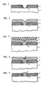
- FIG. 1 depicts a substrate 1, patterned dielectric layer 3 and sidewall spacers 5.
- the sidewall spacers 5 are formed at the edges of an opening in patterned dielectric layer 3 which exposes selected portions of substrate 1.
- the openings are conveniently termed windows and typically have diameters less than approximately 1.0 ⁇ m.
- substrate is used in a broad sense and may comprise silicon or the first level metallization or any other lower level metal interconnection which may be present. The term is thus used to mean the material underlying the dielectric layer 3.
- the dielectric is typically an oxide although other insulators may be used.
- a typical dielectric thickness is approximately 60 nm, but the thickness is not critical for this invention. It will be readily appreciated that devices are present and that there will be many more windows present.
- the sidewall spacers typically comprise an oxide formed by a technique such as that described by K. H. Lee in U.S. Patent 4,641,420 issued on February 10, 1987. Any dielectric that can be formed conformally can be used for the sidewall spacers.
- an aluminum layer 7 is deposited to form the structure depicted in FIG. 2.
- the deposited aluminum layer 7 has a thickness approximately equal to that of the dielectric layer.
- layers may be used having a thickness greater than that of the dielectric layer. It should be noted that the aluminum layer is deposited without any reentrant angles, due to the sidewall spacers, and that the layer has a non-planar surface due to the window. There is a valley in the aluminum layer over the window.
- a layer of photoresist 9 is now deposited and spin coated to yield the essentially planar surface depicted in FIG. 3.
- the photoresist may be any conventional and well known photoresist.
- etching of the photoresist commences, using a first etchant, and continues until a portion of the surface of aluminum layer 7 is reached and exposed. It will be appreciated that no mask is used and there are thus no registration problems. This structure is depicted in FIG. 4.
- the etching conditions are changed and a second etchant is selected which etches only aluminum.
- the remaining photoresist 9 in the Al valley over the window acts as an etching mask and protects the central portion of the aluminum layer on top of the window.
- the etching mask is therefore self-aligned with respect to the window opening. The etching continues until the dielectric surface is exposed, the remaining photoresist is stripped. The resulting contact is depicted in FIG. 5. It should be noted that the contact has an essentially planar surface because some of the aluminum layer underneath the photomask is removed. This is expected from an etching process that is not completely anisotropic in the vertical direction but has some undercutting. Only a single contact is depicted, although it will be readily appreciated, as previously mentioned, that an integrated circuit will have many such contacts.
- FIG. 6 depicts a second level metal runner. Fabrication of this structure is more easily understood by reference to FIGs. 7-9.
- the aluminum deposition continues until the distance, A, from the top of the dielectric layer 3 to the bottom of the aluminum valley is approximately equal to or greater than the desired thickness of the second level metal runner.
- the valley has a depth, B.
- the structure is depicted in FIG. 7. Photoresist is now applied and spin coated to yield a planar surface as depicted in FIG. 8.
- the photoresist and aluminum are now etched, as previously described, until the bottom of the valley is reached.
Landscapes
- Internal Circuitry In Semiconductor Integrated Circuit Devices (AREA)
Applications Claiming Priority (2)
| Application Number | Priority Date | Filing Date | Title |
|---|---|---|---|
| US8108287A | 1987-08-03 | 1987-08-03 | |
| US81082 | 1987-08-03 |
Publications (1)
| Publication Number | Publication Date |
|---|---|
| EP0302647A1 true EP0302647A1 (fr) | 1989-02-08 |
Family
ID=22161994
Family Applications (1)
| Application Number | Title | Priority Date | Filing Date |
|---|---|---|---|
| EP88306847A Withdrawn EP0302647A1 (fr) | 1987-08-03 | 1988-07-26 | Bouchon en aluminium, utilisant un élément de garde de paroi latéral isolant |
Country Status (2)
| Country | Link |
|---|---|
| EP (1) | EP0302647A1 (fr) |
| JP (1) | JPS6459936A (fr) |
Cited By (4)
| Publication number | Priority date | Publication date | Assignee | Title |
|---|---|---|---|---|
| DE3925603A1 (de) * | 1989-08-02 | 1991-02-07 | Siemens Ag | Verfahren zur herstellung von schmalen materialbahnen im (my)m- und sub- (my)m-bereich auf relativ ebenem traegermaterial |
| EP0827195A1 (fr) * | 1996-08-28 | 1998-03-04 | Texas Instruments Inc. | Améliorations relatives aux composants semi-conducteurs |
| WO2003071597A1 (fr) * | 2002-02-21 | 2003-08-28 | Koninklijke Philips Electronics N.V. | Procede de formation de moyens de connexion electriques aux dimensions ideales et dispositif comprenant de tels moyens de connexion |
| US8479641B2 (en) | 2005-12-01 | 2013-07-09 | Koninklijke Philips Electronics N.V. | Tea making device having an improved liquid collection chamber |
Families Citing this family (1)
| Publication number | Priority date | Publication date | Assignee | Title |
|---|---|---|---|---|
| JP4886497B2 (ja) * | 2006-12-18 | 2012-02-29 | キヤノン株式会社 | インクジェット記録ヘッド及びインクジェット記録装置 |
Citations (3)
| Publication number | Priority date | Publication date | Assignee | Title |
|---|---|---|---|---|
| US4489481A (en) * | 1982-09-20 | 1984-12-25 | Texas Instruments Incorporated | Insulator and metallization method for VLSI devices with anisotropically-etched contact holes |
| US4614563A (en) * | 1984-08-02 | 1986-09-30 | Fuji Photo Film Co., Ltd. | Process for producing multilayer conductor structure |
| US4641420A (en) * | 1984-08-30 | 1987-02-10 | At&T Bell Laboratories | Metalization process for headless contact using deposited smoothing material |
Family Cites Families (2)
| Publication number | Priority date | Publication date | Assignee | Title |
|---|---|---|---|---|
| EP0199030A3 (fr) * | 1985-04-11 | 1987-08-26 | Siemens Aktiengesellschaft | Procédé pour fabriquer des interconnexions multicouches pour des circuits intégrés à semi-conducteur comprenant au moins une couche en alliage d'aluminium avec un remplissage du trou de contact |
| JPS6276650A (ja) * | 1985-09-30 | 1987-04-08 | Toshiba Corp | 半導体装置の製造方法 |
-
1988
- 1988-07-26 EP EP88306847A patent/EP0302647A1/fr not_active Withdrawn
- 1988-07-29 JP JP63188546A patent/JPS6459936A/ja active Pending
Patent Citations (3)
| Publication number | Priority date | Publication date | Assignee | Title |
|---|---|---|---|---|
| US4489481A (en) * | 1982-09-20 | 1984-12-25 | Texas Instruments Incorporated | Insulator and metallization method for VLSI devices with anisotropically-etched contact holes |
| US4614563A (en) * | 1984-08-02 | 1986-09-30 | Fuji Photo Film Co., Ltd. | Process for producing multilayer conductor structure |
| US4641420A (en) * | 1984-08-30 | 1987-02-10 | At&T Bell Laboratories | Metalization process for headless contact using deposited smoothing material |
Cited By (4)
| Publication number | Priority date | Publication date | Assignee | Title |
|---|---|---|---|---|
| DE3925603A1 (de) * | 1989-08-02 | 1991-02-07 | Siemens Ag | Verfahren zur herstellung von schmalen materialbahnen im (my)m- und sub- (my)m-bereich auf relativ ebenem traegermaterial |
| EP0827195A1 (fr) * | 1996-08-28 | 1998-03-04 | Texas Instruments Inc. | Améliorations relatives aux composants semi-conducteurs |
| WO2003071597A1 (fr) * | 2002-02-21 | 2003-08-28 | Koninklijke Philips Electronics N.V. | Procede de formation de moyens de connexion electriques aux dimensions ideales et dispositif comprenant de tels moyens de connexion |
| US8479641B2 (en) | 2005-12-01 | 2013-07-09 | Koninklijke Philips Electronics N.V. | Tea making device having an improved liquid collection chamber |
Also Published As
| Publication number | Publication date |
|---|---|
| JPS6459936A (en) | 1989-03-07 |
Similar Documents
| Publication | Publication Date | Title |
|---|---|---|
| US4487652A (en) | Slope etch of polyimide | |
| US6232647B1 (en) | Air gap with borderless contact | |
| US5246883A (en) | Semiconductor contact via structure and method | |
| US4663832A (en) | Method for improving the planarity and passivation in a semiconductor isolation trench arrangement | |
| US4789760A (en) | Via in a planarized dielectric and process for producing same | |
| US20040051183A1 (en) | Method of forming self-aligned contact structure with locally etched gate conductive layer | |
| EP0540446B1 (fr) | Piliers de contact autoalignés pour dispositifs semi-conducteurs | |
| US5500382A (en) | Self-aligned contact process | |
| US5437763A (en) | Method for formation of contact vias in integrated circuits | |
| US5294296A (en) | Method for manufacturing a contact hole of a semiconductor device | |
| KR0176199B1 (ko) | 반도체 소자의 접촉창 형성방법 | |
| EP0369953B1 (fr) | Inclination des parois de trous dans des couches diélectriques pour former des contacts dans des dispositifs intégrés | |
| JPH11186225A (ja) | テーパ形コンタクトホールの形成方法、テーパ形ポリシリコンプラグの形成方法並びにテーパ形ポリシリコンプラグ | |
| US5423939A (en) | Method for forming contact plugs in integrated circuits | |
| US4654119A (en) | Method for making submicron mask openings using sidewall and lift-off techniques | |
| JPH08181205A (ja) | 半導体装置の配線構造およびその製造方法 | |
| US5490901A (en) | Method for forming a contact hole in a semiconductor device | |
| US6949458B2 (en) | Self-aligned contact areas for sidewall image transfer formed conductors | |
| EP0302647A1 (fr) | Bouchon en aluminium, utilisant un élément de garde de paroi latéral isolant | |
| JPH05243193A (ja) | 半導体集積回路における内部接点を露出させる複数のコンタクトホールを形成する方法 | |
| KR20000004334A (ko) | 반도체 소자의 금속배선 형성방법 | |
| JPH0590197A (ja) | 半導体装置の製造方法 | |
| JPH0653334A (ja) | 半導体装置の製造方法 | |
| US5958797A (en) | Planarization of a patterned structure on a substrate using an ion implantation-assisted wet chemical etch | |
| EP0496169A1 (fr) | Procédé pour la fabrication de circuits intégrés comprenant le remplissage d'ouvertures avec un matériau conducteur |
Legal Events
| Date | Code | Title | Description |
|---|---|---|---|
| PUAI | Public reference made under article 153(3) epc to a published international application that has entered the european phase |
Free format text: ORIGINAL CODE: 0009012 |
|
| AK | Designated contracting states |
Kind code of ref document: A1 Designated state(s): DE FR GB IT NL |
|
| STAA | Information on the status of an ep patent application or granted ep patent |
Free format text: STATUS: THE APPLICATION IS DEEMED TO BE WITHDRAWN |
|
| 18D | Application deemed to be withdrawn |
Effective date: 19890809 |