EP0369953B1 - Inclination des parois de trous dans des couches diélectriques pour former des contacts dans des dispositifs intégrés - Google Patents
Inclination des parois de trous dans des couches diélectriques pour former des contacts dans des dispositifs intégrés Download PDFInfo
- Publication number
- EP0369953B1 EP0369953B1 EP89830492A EP89830492A EP0369953B1 EP 0369953 B1 EP0369953 B1 EP 0369953B1 EP 89830492 A EP89830492 A EP 89830492A EP 89830492 A EP89830492 A EP 89830492A EP 0369953 B1 EP0369953 B1 EP 0369953B1
- Authority
- EP
- European Patent Office
- Prior art keywords
- layer
- dielectric
- dielectric material
- dielectric layer
- hole
- Prior art date
- Legal status (The legal status is an assumption and is not a legal conclusion. Google has not performed a legal analysis and makes no representation as to the accuracy of the status listed.)
- Expired - Lifetime
Links
Images
Classifications
-
- H—ELECTRICITY
- H10—SEMICONDUCTOR DEVICES; ELECTRIC SOLID-STATE DEVICES NOT OTHERWISE PROVIDED FOR
- H10W—GENERIC PACKAGES, INTERCONNECTIONS, CONNECTORS OR OTHER CONSTRUCTIONAL DETAILS OF DEVICES COVERED BY CLASS H10
- H10W20/00—Interconnections in chips, wafers or substrates
- H10W20/01—Manufacture or treatment
- H10W20/071—Manufacture or treatment of dielectric parts thereof
- H10W20/081—Manufacture or treatment of dielectric parts thereof by forming openings in the dielectric parts
- H10W20/082—Manufacture or treatment of dielectric parts thereof by forming openings in the dielectric parts the openings being tapered via holes
-
- H—ELECTRICITY
- H10—SEMICONDUCTOR DEVICES; ELECTRIC SOLID-STATE DEVICES NOT OTHERWISE PROVIDED FOR
- H10P—GENERIC PROCESSES OR APPARATUS FOR THE MANUFACTURE OR TREATMENT OF DEVICES COVERED BY CLASS H10
- H10P50/00—Etching of wafers, substrates or parts of devices
- H10P50/20—Dry etching; Plasma etching; Reactive-ion etching
- H10P50/28—Dry etching; Plasma etching; Reactive-ion etching of insulating materials
- H10P50/282—Dry etching; Plasma etching; Reactive-ion etching of insulating materials of inorganic materials
- H10P50/283—Dry etching; Plasma etching; Reactive-ion etching of insulating materials of inorganic materials by chemical means
Definitions
- the present invention relates to a process for forming tapered holes through di electric layers for making electrical contacts in semiconductor integrated devices according to claim 1.
- the proces is particularly useful for fabricating integrated MISFET devices.
- step coverage i.e. to the more or less satisfactory ability to ensure that the metal which is deposited to fill micrometric or sub-micrometric holes etched through a dielectric layer and conformally above the surface of the latter, has the necessary continuity and uniformity of thickness and is not prone to develop fractures in particularly critical points such as on vertical steps and over sharp edges of the surface over which the metal is deposited.
- step coverage i.e. to the more or less satisfactory ability to ensure that the metal which is deposited to fill micrometric or sub-micrometric holes etched through a dielectric layer and conformally above the surface of the latter, has the necessary continuity and uniformity of thickness and is not prone to develop fractures in particularly critical points such as on vertical steps and over sharp edges of the surface over which the metal is deposited.
- taper the contact holes i.e.
- a commonly employed technique for smoothing the rim edge of etch holes through the dielectric contemplates a thermal "reflow" of the dielectric material itself.
- this treatment has the disadvantage of being necessarily carried out during the terminal steps of the process of fabrication of integrated devices and may alter the diffusion profiles of the various doping species relative to regions of the monocrystalline semiconductor substrate already critically defined in devices with a high level of miniaturization.
- the reflow heat treatment of the dielectric may indeed "choke" an etched hole.
- a further proposal has been of carrying out after a first partial anisotropic etching step of the dielectric, a second etching step under isotropic conditions for completing the etching of the residual thickness on the bottom of the etch hole and simultaneously causing a tapering of the top portion of the hole pre-etched through the thickness of the dielectric material layer (round etch). Also this technique has problems relating to maintaining satisfactory dimensional control.
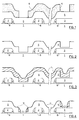
- FIGS 1 to 4 illustrate the process of the invention.
- the example shown in the figures relates to the case of a semiconductor integrated MOS device wherein on a semiconducting substrate of monocrystalline silicon 1 (wherein diffused regions, not shown in the figures, have already been formed as customary) conducting gate tracks 2 of polycrystalline silicon (polysilicon) are formed, disposed in a matrix type arrangement and which are insulated from the silicon 1 by means of a dielectric gate layer 8, while other polysilicon tracks 3 are also formed in peripheral areas. All the conducting tracks 2 and 3 of a "first level" polysilicon are commonly tapered a long their sides by means of dielectric spacers 4 of silicon oxide which are formed according to techniques which are well known to a skilled technician. The layer of insulating dielectric material through which contacts must be formed is indicated with 5 in the figures.
- a photoresist mask 6 is formed, through which the contacts to be formed are photolithographically defined in a substantially noncritical way because, as it will become evident through the following description, the contacts may be defined through the photoresist mask 6 with magnified dimensions, i.e. with relatively lessened dimensional tolerances. This step is depicted in Fig. 1.
- a second layer 7 of dielectric material is then deposited in an essentially conformal way and with a thickness comprised between about 4500 and 6500 Angstroms.
- Tetra-Ethyl Ortho Silicate (TEOS) is the preferred precursor material used to deposit this second dielectric layer 7.
- a second RIE plasma etching (substantially anisotropic etching as the first etch) of this second layer of dielectric material 7 deposited in a conformal way, is then performed and the etching is continued until etching off completely the residual layer of dielectric material 5 previously left on the bottom of the previously etched holes and until exposing the underlying monocrystalline silicon substrate 1 in the area C1 defined for a "low” contact and/or the polysilicon 3 within an area C2 defined for a "high” contact, as shown in Fig. 4.
- the process of the instant invention thus attains the objective and results extremely efficient and advantageous.
Landscapes
- Internal Circuitry In Semiconductor Integrated Circuit Devices (AREA)
- Drying Of Semiconductors (AREA)
- Electrodes Of Semiconductors (AREA)
Claims (6)
- Procédé de formation d'un trou à parois inclinées à travers une couche diélectrique pour réaliser un contact électrique dans un dispositif semiconducteur intégré qui comprend les étapes suivantes :a) prévoir un substrat semiconducteur ou conducteur portant une première couche diélectrique ;b) graver de façon anisotrope la première couche diélectrique dans un plasma RIE à travers un masque définissant un trou de contact pour former ainsi au moins un trou gravé, cette gravure étant réalisée jusqu'à une profondeur inférieure à l'épaisseur de la couche, laissant ainsi une épaisseur résiduelle du premier matériau diélectrique au fond dudit au moins un trou gravé ;c) enlever le matériau résiduel du masque de contact ;d déposer de façon conforme une seconde couche de matériau diélectrique sur l'épaisseur résiduelle du matériau diélectrique ;e) graver de façon anisotrope sans masquage dans un plasma RIE la seconde couche de matériau diélectrique et la première couche diélectrique sous-jacente à la seconde couche jusqu'à une épaisseur sensiblement égale à l'épaisseur résiduelle au fond du trou gravé pour exposer ainsi la surface du substrat semiconducteur ou conducteur sous-jacent à la première couche diélectrique et avec lequel le contact électrique doit ensuite être assuré, tout en laissant sur une paroi sensiblement verticale du trou gravé à travers la première couche diélectrique un résidu à parois inclinées du matériau diélectrique de la seconde couche de matériau diélectrique.
- Procédé selon la revendication 1, dans lequel l'épaisseur résiduelle de matériau diélectrique est d'environ 1000 à 2000 angstroems (100 à 200 nm).
- Procédé selon la revendication 2, caractérisé en ce que la seconde couche a une épaisseur comprise entre environ 4500 et 6500 angstroems (450 à 650 nm).
- Procédé selon la revendication 1, comprenant l'étape consistant à déposer du tétraéthylorthosilicate pour former la seconde couche.
- Procédé selon la revendication 1, dans lequel la première couche diélectrique est de l'oxyde de silicium.
- Procédé selon la revendication 1, dans lequel le substrat est du silicium monocristallin.
Applications Claiming Priority (2)
| Application Number | Priority Date | Filing Date | Title |
|---|---|---|---|
| IT8368288 | 1988-11-16 | ||
| IT8883682A IT1225631B (it) | 1988-11-16 | 1988-11-16 | Rastremazione di fori attraverso strati dielettrici per formare contatti in dispositivi integrati. |
Publications (2)
| Publication Number | Publication Date |
|---|---|
| EP0369953A1 EP0369953A1 (fr) | 1990-05-23 |
| EP0369953B1 true EP0369953B1 (fr) | 1994-03-23 |
Family
ID=11323793
Family Applications (1)
| Application Number | Title | Priority Date | Filing Date |
|---|---|---|---|
| EP89830492A Expired - Lifetime EP0369953B1 (fr) | 1988-11-16 | 1989-11-13 | Inclination des parois de trous dans des couches diélectriques pour former des contacts dans des dispositifs intégrés |
Country Status (5)
| Country | Link |
|---|---|
| US (1) | US5227014A (fr) |
| EP (1) | EP0369953B1 (fr) |
| JP (1) | JPH02183534A (fr) |
| DE (1) | DE68914099T2 (fr) |
| IT (1) | IT1225631B (fr) |
Families Citing this family (14)
| Publication number | Priority date | Publication date | Assignee | Title |
|---|---|---|---|---|
| US4996167A (en) * | 1990-06-29 | 1991-02-26 | At&T Bell Laboratories | Method of making electrical contacts to gate structures in integrated circuits |
| DE4331549A1 (de) * | 1993-09-16 | 1995-04-13 | Gold Star Electronics | Verfahren zur Herstellung einer ULSI-Halbleitereinrichtung |
| US5756397A (en) * | 1993-12-28 | 1998-05-26 | Lg Semicon Co., Ltd. | Method of fabricating a wiring in a semiconductor device |
| KR0151048B1 (ko) * | 1995-05-24 | 1998-12-01 | 김광호 | 반도체 장치의 접촉창 형성방법 |
| US5686354A (en) * | 1995-06-07 | 1997-11-11 | Advanced Micro Devices, Inc. | Dual damascene with a protective mask for via etching |
| US5567270A (en) * | 1995-10-16 | 1996-10-22 | Winbond Electronics Corp. | Process of forming contacts and vias having tapered sidewall |
| US6111319A (en) | 1995-12-19 | 2000-08-29 | Stmicroelectronics, Inc. | Method of forming submicron contacts and vias in an integrated circuit |
| US5847460A (en) * | 1995-12-19 | 1998-12-08 | Stmicroelectronics, Inc. | Submicron contacts and vias in an integrated circuit |
| US5883006A (en) * | 1997-12-12 | 1999-03-16 | Kabushiki Kaisha Toshiba | Method for making a semiconductor device using a flowable oxide film |
| TW449828B (en) * | 1998-08-24 | 2001-08-11 | United Microelectronics Corp | Method for etching oxide layer with a medium/low plasma density |
| US7531367B2 (en) * | 2006-01-18 | 2009-05-12 | International Business Machines Corporation | Utilizing sidewall spacer features to form magnetic tunnel junctions in an integrated circuit |
| CN101587838B (zh) | 2008-05-23 | 2011-03-23 | 中芯国际集成电路制造(北京)有限公司 | 在电介质层上形成孔的方法 |
| US11661335B2 (en) * | 2020-05-22 | 2023-05-30 | Magic Leap, Inc. | Method and system for scanning MEMS cantilevers |
| US11776844B2 (en) * | 2021-03-24 | 2023-10-03 | Globalfoundries Singapore Pte. Ltd. | Contact via structures of semiconductor devices |
Citations (1)
| Publication number | Priority date | Publication date | Assignee | Title |
|---|---|---|---|---|
| EP0226890A1 (fr) * | 1985-12-17 | 1987-07-01 | Siemens Aktiengesellschaft | Procédé de fabrication de structures de transistors bipolaires auto-alignés à résistance de base réduite |
Family Cites Families (9)
| Publication number | Priority date | Publication date | Assignee | Title |
|---|---|---|---|---|
| US4472240A (en) * | 1981-08-21 | 1984-09-18 | Tokyo Shibaura Denki Kabushiki Kaisha | Method for manufacturing semiconductor device |
| JPS6058635A (ja) * | 1983-09-12 | 1985-04-04 | Toshiba Corp | 半導体装置の製造方法 |
| JPS6126240A (ja) * | 1984-07-17 | 1986-02-05 | Hitachi Ltd | 絶縁分離方法 |
| US4656732A (en) * | 1984-09-26 | 1987-04-14 | Texas Instruments Incorporated | Integrated circuit fabrication process |
| US4657628A (en) * | 1985-05-01 | 1987-04-14 | Texas Instruments Incorporated | Process for patterning local interconnects |
| US4660278A (en) * | 1985-06-26 | 1987-04-28 | Texas Instruments Incorporated | Process of making IC isolation structure |
| JPH0789562B2 (ja) * | 1985-11-01 | 1995-09-27 | 富士通株式会社 | 集積回路の素子分離方法 |
| US4707218A (en) * | 1986-10-28 | 1987-11-17 | International Business Machines Corporation | Lithographic image size reduction |
| JPS63293946A (ja) * | 1987-05-27 | 1988-11-30 | Matsushita Electric Ind Co Ltd | 半導体装置の製造方法 |
-
1988
- 1988-11-16 IT IT8883682A patent/IT1225631B/it active
-
1989
- 1989-11-13 EP EP89830492A patent/EP0369953B1/fr not_active Expired - Lifetime
- 1989-11-13 DE DE68914099T patent/DE68914099T2/de not_active Expired - Fee Related
- 1989-11-14 US US07/435,890 patent/US5227014A/en not_active Expired - Lifetime
- 1989-11-16 JP JP1298747A patent/JPH02183534A/ja active Pending
Patent Citations (1)
| Publication number | Priority date | Publication date | Assignee | Title |
|---|---|---|---|---|
| EP0226890A1 (fr) * | 1985-12-17 | 1987-07-01 | Siemens Aktiengesellschaft | Procédé de fabrication de structures de transistors bipolaires auto-alignés à résistance de base réduite |
Also Published As
| Publication number | Publication date |
|---|---|
| DE68914099D1 (de) | 1994-04-28 |
| JPH02183534A (ja) | 1990-07-18 |
| IT8883682A0 (it) | 1988-11-16 |
| US5227014A (en) | 1993-07-13 |
| IT1225631B (it) | 1990-11-22 |
| EP0369953A1 (fr) | 1990-05-23 |
| DE68914099T2 (de) | 1994-07-07 |
Similar Documents
| Publication | Publication Date | Title |
|---|---|---|
| US4502914A (en) | Method of making structures with dimensions in the sub-micrometer range | |
| EP0345875B1 (fr) | Procédé de fabrication d'un dispositif semi-conducteur | |
| US6033980A (en) | Method of forming submicron contacts and vias in an integrated circuit | |
| US8552526B2 (en) | Self-aligned semiconductor trench structures | |
| US6171951B1 (en) | Dual damascene method comprising ion implanting to densify dielectric layer and forming a hard mask layer with a tapered opening | |
| US5895255A (en) | Shallow trench isolation formation with deep trench cap | |
| JPH01290236A (ja) | 幅の広いトレンチを平坦化する方法 | |
| US5342808A (en) | Aperture size control for etched vias and metal contacts | |
| JPH0217637A (ja) | 高度に平面化された集積回路構造を作るための方法 | |
| USRE38363E1 (en) | Method of forming trench isolation having polishing step and method of manufacturing semiconductor device | |
| US5227014A (en) | Tapering of holes through dielectric layers for forming contacts in integrated devices | |
| JP4057083B2 (ja) | 半導体集積回路の製造方法 | |
| US4708770A (en) | Planarized process for forming vias in silicon wafers | |
| US4584761A (en) | Integrated circuit chip processing techniques and integrated chip produced thereby | |
| KR0176199B1 (ko) | 반도체 소자의 접촉창 형성방법 | |
| US6278189B1 (en) | High density integrated circuits using tapered and self-aligned contacts | |
| US6740574B2 (en) | Methods of forming DRAM assemblies, transistor devices, and openings in substrates | |
| US5966632A (en) | Method of forming borderless metal to contact structure | |
| US6278161B1 (en) | Transistor | |
| KR0165453B1 (ko) | Y자형 트랜치를 이용한 반도체 소자의 분리 방법 | |
| KR100269595B1 (ko) | 프로파일을 개선한 콘택홀의 제조방법 | |
| KR100278883B1 (ko) | 반도체 소자 분리를 위한 얕은 트렌치 제조 방법 | |
| US6114237A (en) | Method of forming contacts for a semiconductor device | |
| KR100338091B1 (ko) | 반도체소자제조방법 | |
| KR0166134B1 (ko) | 반도체 소자의 게이트 전극 형성 방법 |
Legal Events
| Date | Code | Title | Description |
|---|---|---|---|
| PUAI | Public reference made under article 153(3) epc to a published international application that has entered the european phase |
Free format text: ORIGINAL CODE: 0009012 |
|
| AK | Designated contracting states |
Kind code of ref document: A1 Designated state(s): DE FR GB NL SE |
|
| 17P | Request for examination filed |
Effective date: 19900709 |
|
| 17Q | First examination report despatched |
Effective date: 19920402 |
|
| GRAA | (expected) grant |
Free format text: ORIGINAL CODE: 0009210 |
|
| AK | Designated contracting states |
Kind code of ref document: B1 Designated state(s): DE FR GB NL SE |
|
| REF | Corresponds to: |
Ref document number: 68914099 Country of ref document: DE Date of ref document: 19940428 |
|
| ET | Fr: translation filed | ||
| PLBE | No opposition filed within time limit |
Free format text: ORIGINAL CODE: 0009261 |
|
| STAA | Information on the status of an ep patent application or granted ep patent |
Free format text: STATUS: NO OPPOSITION FILED WITHIN TIME LIMIT |
|
| EAL | Se: european patent in force in sweden |
Ref document number: 89830492.8 |
|
| 26N | No opposition filed | ||
| REG | Reference to a national code |
Ref country code: FR Ref legal event code: D6 |
|
| PGFP | Annual fee paid to national office [announced via postgrant information from national office to epo] |
Ref country code: SE Payment date: 20011106 Year of fee payment: 13 |
|
| PGFP | Annual fee paid to national office [announced via postgrant information from national office to epo] |
Ref country code: FR Payment date: 20011113 Year of fee payment: 13 |
|
| PGFP | Annual fee paid to national office [announced via postgrant information from national office to epo] |
Ref country code: GB Payment date: 20011114 Year of fee payment: 13 |
|
| PGFP | Annual fee paid to national office [announced via postgrant information from national office to epo] |
Ref country code: DE Payment date: 20011126 Year of fee payment: 13 |
|
| PGFP | Annual fee paid to national office [announced via postgrant information from national office to epo] |
Ref country code: NL Payment date: 20011129 Year of fee payment: 13 |
|
| REG | Reference to a national code |
Ref country code: GB Ref legal event code: IF02 |
|
| PG25 | Lapsed in a contracting state [announced via postgrant information from national office to epo] |
Ref country code: GB Free format text: LAPSE BECAUSE OF NON-PAYMENT OF DUE FEES Effective date: 20021113 |
|
| PG25 | Lapsed in a contracting state [announced via postgrant information from national office to epo] |
Ref country code: SE Free format text: LAPSE BECAUSE OF NON-PAYMENT OF DUE FEES Effective date: 20021114 |
|
| PG25 | Lapsed in a contracting state [announced via postgrant information from national office to epo] |
Ref country code: NL Free format text: LAPSE BECAUSE OF NON-PAYMENT OF DUE FEES Effective date: 20030601 |
|
| PG25 | Lapsed in a contracting state [announced via postgrant information from national office to epo] |
Ref country code: DE Free format text: LAPSE BECAUSE OF NON-PAYMENT OF DUE FEES Effective date: 20030603 |
|
| EUG | Se: european patent has lapsed | ||
| GBPC | Gb: european patent ceased through non-payment of renewal fee | ||
| PG25 | Lapsed in a contracting state [announced via postgrant information from national office to epo] |
Ref country code: FR Free format text: LAPSE BECAUSE OF NON-PAYMENT OF DUE FEES Effective date: 20030731 |
|
| NLV4 | Nl: lapsed or anulled due to non-payment of the annual fee |
Effective date: 20030601 |
|
| REG | Reference to a national code |
Ref country code: FR Ref legal event code: ST |