EP0302659B1 - Dispositif semi-conducteur à mémoire et son procédé de fabrication - Google Patents
Dispositif semi-conducteur à mémoire et son procédé de fabrication Download PDFInfo
- Publication number
- EP0302659B1 EP0302659B1 EP88306931A EP88306931A EP0302659B1 EP 0302659 B1 EP0302659 B1 EP 0302659B1 EP 88306931 A EP88306931 A EP 88306931A EP 88306931 A EP88306931 A EP 88306931A EP 0302659 B1 EP0302659 B1 EP 0302659B1
- Authority
- EP
- European Patent Office
- Prior art keywords
- gate
- insulating film
- regions
- type
- substrate
- Prior art date
- Legal status (The legal status is an assumption and is not a legal conclusion. Google has not performed a legal analysis and makes no representation as to the accuracy of the status listed.)
- Expired - Lifetime
Links
- 239000004065 semiconductor Substances 0.000 title claims description 38
- 238000000034 method Methods 0.000 title claims description 21
- 239000000758 substrate Substances 0.000 claims description 45
- 239000012535 impurity Substances 0.000 claims description 20
- 238000005468 ion implantation Methods 0.000 claims description 6
- 239000000126 substance Substances 0.000 claims description 5
- 239000002344 surface layer Substances 0.000 claims description 5
- 230000006870 function Effects 0.000 claims description 4
- 230000000873 masking effect Effects 0.000 claims description 3
- 239000011159 matrix material Substances 0.000 claims description 3
- 230000015654 memory Effects 0.000 description 12
- 239000011295 pitch Substances 0.000 description 10
- 230000003647 oxidation Effects 0.000 description 5
- 238000007254 oxidation reaction Methods 0.000 description 5
- 229910021420 polycrystalline silicon Inorganic materials 0.000 description 5
- 229910052751 metal Inorganic materials 0.000 description 4
- 239000002184 metal Substances 0.000 description 4
- 229920005591 polysilicon Polymers 0.000 description 4
- 239000011229 interlayer Substances 0.000 description 3
- ZOXJGFHDIHLPTG-UHFFFAOYSA-N Boron Chemical compound [B] ZOXJGFHDIHLPTG-UHFFFAOYSA-N 0.000 description 2
- VYPSYNLAJGMNEJ-UHFFFAOYSA-N Silicium dioxide Chemical compound O=[Si]=O VYPSYNLAJGMNEJ-UHFFFAOYSA-N 0.000 description 2
- XUIMIQQOPSSXEZ-UHFFFAOYSA-N Silicon Chemical compound [Si] XUIMIQQOPSSXEZ-UHFFFAOYSA-N 0.000 description 2
- 229910052796 boron Inorganic materials 0.000 description 2
- 239000002019 doping agent Substances 0.000 description 2
- 239000000463 material Substances 0.000 description 2
- 150000002739 metals Chemical class 0.000 description 2
- 229910052710 silicon Inorganic materials 0.000 description 2
- 239000010703 silicon Substances 0.000 description 2
- OAICVXFJPJFONN-UHFFFAOYSA-N Phosphorus Chemical compound [P] OAICVXFJPJFONN-UHFFFAOYSA-N 0.000 description 1
- 229910052581 Si3N4 Inorganic materials 0.000 description 1
- QVGXLLKOCUKJST-UHFFFAOYSA-N atomic oxygen Chemical compound [O] QVGXLLKOCUKJST-UHFFFAOYSA-N 0.000 description 1
- 239000005380 borophosphosilicate glass Substances 0.000 description 1
- 238000005229 chemical vapour deposition Methods 0.000 description 1
- 229910052681 coesite Inorganic materials 0.000 description 1
- 229910052906 cristobalite Inorganic materials 0.000 description 1
- 239000013078 crystal Substances 0.000 description 1
- 238000009792 diffusion process Methods 0.000 description 1
- 230000005684 electric field Effects 0.000 description 1
- 239000007789 gas Substances 0.000 description 1
- 230000000415 inactivating effect Effects 0.000 description 1
- 230000002779 inactivation Effects 0.000 description 1
- 239000010410 layer Substances 0.000 description 1
- 238000001459 lithography Methods 0.000 description 1
- 238000004519 manufacturing process Methods 0.000 description 1
- 238000002844 melting Methods 0.000 description 1
- 230000008018 melting Effects 0.000 description 1
- 229910052750 molybdenum Inorganic materials 0.000 description 1
- 229910052760 oxygen Inorganic materials 0.000 description 1
- 239000001301 oxygen Substances 0.000 description 1
- 230000002093 peripheral effect Effects 0.000 description 1
- 229910052698 phosphorus Inorganic materials 0.000 description 1
- 239000011574 phosphorus Substances 0.000 description 1
- 238000001259 photo etching Methods 0.000 description 1
- 238000005240 physical vapour deposition Methods 0.000 description 1
- 229910052697 platinum Inorganic materials 0.000 description 1
- 238000000926 separation method Methods 0.000 description 1
- 229910021332 silicide Inorganic materials 0.000 description 1
- 239000000377 silicon dioxide Substances 0.000 description 1
- 235000012239 silicon dioxide Nutrition 0.000 description 1
- 229910052682 stishovite Inorganic materials 0.000 description 1
- 229910052719 titanium Inorganic materials 0.000 description 1
- 229910052905 tridymite Inorganic materials 0.000 description 1
- 229910052721 tungsten Inorganic materials 0.000 description 1
Images

Classifications
-
- H—ELECTRICITY
- H10—SEMICONDUCTOR DEVICES; ELECTRIC SOLID-STATE DEVICES NOT OTHERWISE PROVIDED FOR
- H10B—ELECTRONIC MEMORY DEVICES
- H10B41/00—Electrically erasable-and-programmable ROM [EEPROM] devices comprising floating gates
-
- H—ELECTRICITY
- H10—SEMICONDUCTOR DEVICES; ELECTRIC SOLID-STATE DEVICES NOT OTHERWISE PROVIDED FOR
- H10B—ELECTRONIC MEMORY DEVICES
- H10B20/00—Read-only memory [ROM] devices
Definitions
- the present invention relates to semiconductor memory devices, and more particularly to read-only memories (hereinafter referred to as "ROMs").
- ROMs read-only memories
- ROMs for use in storing various items of program data generally comprise a plurality of MIS transistors in the form of a matrix of gate wiring and source and drain regions.
- Such ROMs are, in a predetermined manner, either open-circuit between the source and drain regions of the transistors, or short-circuited between the source and drain regions, or inactivated between the source and drain regions with increased thickness of insulating film under the gate wiring (i.e., gate insulating film), whereby currents between the drain and the source are detected or non-detected and hence the memory data unit "1" or "0" is stored.
- a ROM device is known from US-A-4 342 100.
- LOCOS Local Oxidation Silicon
- MOS Device Complete Book of Electronics Techniques, pp. 290-291 Kogyo Chosakai (Industrial Research Association), (1976)
- Figure 2 (a) is a plan view of a conventional silicon-gate ROM
- Figure 2 (b) is a view in section taken along the line A-A' in Figure 2 (a)
- Figure 2 (c) is a view in section taken along the line B-B' in Figure 2 (a).
- Oxide films 2a and 2b are formed by the LOCOS process on the cell separating regions and inactive transistor gate regions of a semiconductor substrate 1.
- a gate oxide film 3 is formed on the gate regions of the semiconductor substrate providing active transistors.
- Gate wiring 4 of polysilicon is then formed on the substrate 1, and semiconductor regions providing source regions 5a and drain regions 5b are thereafter formed on the substrate 1 using the oxide films 2a, 2b and the gate wiring 4 for masking.
- an interlayer insulating film 6 of NSG, BPSG or the like is formed on the substrate 1, contact holes 7 are formed in the interlayer insulating film 6 on the drain regions 5b, and metal wiring 8 is thereafter provided in contact with the drain regions 5b.
- the oxide film 2b having a larger thickness than the gate film 3 is formed in the gate regions ( ⁇ ) of the inactive transistors by the LOCOS process, so that when such a transistor is selected for reading out data, no current flows between the source region 5a and the drain region 5b.
- the film formed invariably has a larger width than is intended owing to the influence of internal diffusion of oxygen during thermal oxidation.
- the ratio of increase in the width is greater when the specified width is smaller.
- ROM cells having such a thick insulating film in the cell separating region and as the gate inactivating film are limited in design by the increase in the film width, which imposes limitations on the provision of ROMs of greater complexity.
- the horizontal pitch required is 3.6 ⁇ m, which is the total of 1 ⁇ m for a space a for the contact hole 7, 0.4 ⁇ m for each of two portions of allowance b for the alignment of the contact hole 7 with the drain region 5b, 0.4 ⁇ m for each of two edge portions c of the oxide film 2a formed by the LOCOS process and providing a cell separating region, and 1 ⁇ m for a space d for the oxide film 2a formed by the LOCOS process and providing a cell separating region.
- the vertical pitch for the active transistor is 3.2 ⁇ m, which is the total of 0.5 ⁇ m for a half portion A of the source region 5a, 0.8 ⁇ m for an allowance B for the alignment of the gate 4 with the source area 5a, 1 ⁇ m for the width C of the gate 4, 0.4 ⁇ m for an allowance D for aligning the gate 4 with the contact hole 7, and 0.5 ⁇ m for one half portion E of the contact hole 7.
- the vertical pitch is 3.2 ⁇ m, which is the total of 0.5 ⁇ m for the other half portion E of the contact hole 7, 0.4 ⁇ m for an allowance D for aligning the gate wiring 4 with the contact hole 7, 0.4 ⁇ m for each of two edge portions F of the oxide film 2b formed by the LOCOS process in the gate region of the inactive transistor, 1 ⁇ m for a space G for the oxide film 2b, and 0.5 ⁇ m for a half portion A of the source region 5a.
- the pitch required is 3.2 ⁇ m regardless of whether the transistor is active or inactive.
- the main object of the present invention which has been accomplished to overcome the above problem, is to provide a semiconductor memory device which is remarkably improved in complexity over conventional ones.
- the invention provides a semiconductor memory device comprising:
- a method of reading a device as described above comprising: simultaneously applying a first voltage (selection voltage) to a selected gate electrode sufficient to make conducting the transistors associated therewith that have not been selectively doped to said higher concentration and insufficient to make conducting the transistors associated therewith that have been selectively doped to said higher concentration; and applying a second voltage (reference voltage) to at least those gate electrodes immediately adjacent to said selected gate electrode sufficient to make the transistors associated with said adjacent gate electrodes non-conductive so that the semiconductor surface region under said adjacent gate electrodes functions as a cell separating region.
- a first voltage selection voltage
- second voltage reference voltage
- the invention further provides a process for producing a semiconductor memory device comprising the steps of:
- the present invention has been accomplished directing attention to the following.
- the transistors concerned can be inactivated without forming a thick insulating film.
- the non-selected gate electrodes other than the selected gate electrodes are given a potential which renders the transistors under the non-selected gate electrodes non-conductive, so that the semiconductor surface region under the non-selected gate electrode adjacent to the selected gate electrode can be made to function as a kind of cell separating region.
- the cell (transistor) having a gate region doped with impurities at a high concentration has a higher threshold gate voltage Vth than the one not doped to the high concentration.
- the difference results in the following.
- a voltage (selection voltage) higher than the threshold voltage A but lower than the threshold voltage B of the former transistor is applied to one of the electrodes.
- the transistor not having the high dopant concentration is then brought into conduction, whereas the highly doped transistor remains non-conductive.
- the former state corresponds to the memory data unit, for example, of "1", and the latter to the memory data unit, for example of "0".
- the device of the invention which does not require the conventional cell separating region is greatly reduced in the required area per transistor. This makes it possible to integrate transistors with greater complexity and to provide compacted ROM memory cells.
- the first and second gate insulating films according to the invention can be usual gate insulating films of SiO2, Si3N4 or the like. It is suitable that these films be 10 nm (100 angstroms) to 100 nm (1000 angstroms) in thickness in view of the insulating property and application of an electric field.
- the films can be formed by the usual thermal oxidation method, CVD method, etc.
- the second gate insulating film is so formed as to cover each edge portion of the gate electrode which is formed in the shape of a strip having a specified width on each strip of first gate insulating film. This is desirable to inhibit or diminish the leakage current between the cells.
- the first and second gate electrodes of the invention are formed each in the form of a strip on the first and second gate insulating films, respectively.
- suitable materials for forming these electrodes are A1 and the like metals, polycrystalline silicon, metals, such as W, Ti, Pt and Mo, having a high melting point, and silicides thereof such as WSi, WSi and WTiSI.
- the semiconductor substrate to be used in the invention can be made of various materials generally used in the art. Usually Si substrates are suitable.
- the group of semiconductor regions opposite to the substrate in conductivity, each group of insulating film strips, and each group of gate electrodes can be formed by usual methods as by lithography. The number of lines thereof can be determined suitably in accordance with the contemplated memory capacity.
- the impurity substance for doping the selected gate regions at a high concentration is of the same conductivity type as the substrate.
- the high concentration is about 102 to about 105 times the impurity concentration of the substrate. It is usually suitable to accomplish such high-concentration doping by ion implantation.
- the semiconductor memory device of the invention may have attached thereto a portion or circuit, such as external wiring or external insulating film formed with contact holes for the gate electrodes.
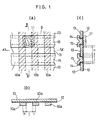
- Figure 1 (a) is a plan view showing an embodiment of the invention
- Figure 1 (b) is a view in section taken along the line A-A' in Figure 1 (a)
- Figure 1 (c) is a view in section taken along the line B-B' therein.
- impurity regions 10 are formed which provide source regions 10a and drain regions 10b.
- the semiconductor substrate used for the present embodiment is a p-type silicon single-crystal substrate containing 7 x 10¹⁴ ats. /cm3 of p-type impurities (boron).
- the impurity regions 10, which are of the second conductivity type, are formed in the surface layer of the substrate 9 approximately in parallel by the ion implantation of n-type impurities (phosphorus at a concentration of 1 x 10²⁰ ats./cm3).
- impurity regions 11 of the first conductivity type of square pattern are selectively locally formed in the spaces (gate regions) between the source regions 10a and the drain regions 10b of the substrate 9.
- a first gate oxide film 12 is then formed substantially over the entire surface of the resulting substrate 9.
- the impurity (high-concentration) regions 11 are formed by the ion implantation of boron at about 1000 times (7 x 1017 ats./cm3) the concentration of the substrate.
- the gate oxide film 12 is formed by thermal oxidation in dry O2 gas and is about 20 nm (200 angstroms) in thickness.
- the impurity regions 11 of the first conductivity type may be formed after forming second gate wiring, by ion implantation.
- pieces of first gate wiring 13 of polysilicon are formed by the CVD process on the first gate oxide film 12 over the substrate 9, approximately in parallel to intersect the impurity regions 10 of the second conductivity type.
- the first gate oxide film 12 is then etched away from the portions of the substrate 9 which are left uncovered by the first gate wiring 13 to expose the substrate portions.
- the second gate oxide film 14 covers not only the exposed surface portions of the substrate 9 but also the edge portions of the first gate wiring 13 as illustrated.
- second gate wiring 15 of polysilicon is formed by the CVD process between the pieces of first gate wiring 13.
- the second gate wiring 15 is provided not only between the wiring portions 13, but also over the opposed side faces of the wiring 13. Subsequently, the second gate oxide film 14 left uncovered by the second gate wiring 15 is etched away.
- An interlayer insulating film, contact holes and metal wiring are thereafter formed by the known CVD process, photoetching and PVD process on the substrate 9 which is almost covered with the first gate wiring 13 and second gate wiring 15 to obtain a masked ROM having double-layer polysilicon gates.
- the second gate wiring 15 of the above embodiment extends over the side faces of the first gate wiring 13, the wiring 15 can be formed without being so extended.
- the transistor having as its channel the impurity region 11 of the first conductivity type doped with impurities of the same conductivity type as those in the semiconductor substrate 9 has a higher threshold voltage than the one free from impurity dopant and remains non-conductive even if selected by application, for example, of a gate voltage of 5 V. Accordingly, the gate regions can be made to correspond to the memory data unit of "1" or "0" in accordance with the presence or absence of the impurity region of the first conductivity type.
- the ROM of the invention described above must have the following dimensions when conforming to the 1.0- ⁇ m rule.
- the horizontal pitch required is 2 ⁇ m, which is the total of 0.5 ⁇ m for a half portion h of the source region 10a, 0.5 ⁇ m for a half portion i of the drain region 10b and 1 ⁇ m for the spacing (gate region) j between the source region 10a and the drain region 10b.
- the vertical pitch required for the transistor having the first gate 13 is 1.4 ⁇ m, which is the total of 1.0 ⁇ m for the width H of the first gate 13, and 0.4 ⁇ m for two half portions I of the lap of the second gate 15 over the first gate 13.
- the vertical pitch required for the transistor having the second gate 15 is 1.4 ⁇ m, which is the total of 1.0 ⁇ m for the width J of the second gate 15, and 0.4 ⁇ m for two half portions I of the lap of the second gate 15 over the first gate 13.
- the vertical pitch required is 1.4 ⁇ m regardless of the gate of the transistor. Since the contacts can be provided concentrically at the peripheral portion of the memory, the area required for the contacts exerts no influence on the memory cells.
- the transistor pitch is, for example, 2 ⁇ m horizontally and 1.4 ⁇ m vertically, hence exceedingly smaller than the conventional ones in the area required. More specifically, in the case of the 1.0- ⁇ m rule, the area of the cell of the invention is 2.8 ⁇ m2 which is about 1 ⁇ 4 of the area 11.52 ⁇ m2 conventionally needed as already mentioned.
- the invention provides ROMs of much higher complexity than heretofore available which are suited as ROMs of 8 Mbits, 16 Mbits or higher complexity.
Landscapes
- Semiconductor Memories (AREA)
Claims (6)
- Dispositif de mémoire à semi-conducteur comportant :(a) un substrat semi-conducteur de type p (ou de type n),(b) un groupe de régions semi-conductrices de type n (ou de type p) formées dans la couche superficielle du substrat sous la forme de bandes disposées en parallèle suivant un espacement prédéterminé, les régions semi-conductrices fournissant des régions de source et des régions de drain alternées et définissant des régions de porte entre les régions alternées,(c) un groupe de bandes d'un premier film d'isolation de porte formées sur la surface du substrat suivant un espacement prédéterminé et intersectant le groupe de régions semi-conductrices,(d) une première électrode de porte formée sur chacune des bandes du premier film d'isolation de porte,(e) un second film d'isolation de porte ayant sensiblement la même épaisseur que celle du premier film d'isolation de porte formé sur la partie de la surface du substrat qui n'est pas recouverte par le premier film d'isolation de porte, et(f) une seconde électrode de porte formée sur chacune des bandes du second film d'isolation de porte et maintenue hors de contact avec la première électrode de porte,
une matrice de cellules de transistor MIS étant formée, une cellule étant formée au niveau de chaque intersection entre l'une des régions de porte et l'une des premières ou l'une des secondes électrodes, les régions de porte de certaines des cellules étant dopées de façon sélective avec une impureté de type p (ou de type n) suivant une concentration supérieure à celle du substrat. - Dispositif selon la revendication 1, dans lequel le second film d'isolation de porte recouvre les bords des premières électrodes de porte qui sont adjacentes à celui-ci.
- Dispositif selon la revendication 1, dans lequel la région superficielle semi-conductrice se trouvant sous l'électrode de porte non sélectionnée adjacente à chaque électrode de porte sélectionnée fonctionne en tant que région de séparation de cellules.
- Procédé de fabrication d'un dispositif de mémoire à semi-conducteur comportant les étapes consistant :(a) à former une multiplicité de régions semi-conductrices de type n (ou de type p) sous la forme de bandes parallèles dans la couche superficielle d'un substrat semi-conducteur de type p (ou de type n), les régions semi-conductrices fournissant des régions de source et des régions de drain alternées et definissant des régions de porte entre elles, et un premier film d'isolation étant formé sur sensiblement toute la surface du substrat semi-conducteur,(b) à former sur le premier film d'isolation une multiplicité de premières électrodes de porte sous la forme de bandes parallèles intersectant les régions semi-conductrices,(c) à enlever le premier film d'isolation des parties de surface du substrat se trouvant entre les premières électrodes de porte en utilisant les électrodes aux fins de masquage pour former des bandes de premier film d'isolation de porte,(d) à former un second film d'isolation, ayant sensiblement la même épaisseur que celle du premier film d'isolation de porte, sur la partie de la surface du substrat qui n'est pas recouverte par le premier film d'isolation de porte, et(e) à former une seconde électrode de porte sur chaque partie du second film d'isolation,
les régions de porte de cellules formées par les intersections des régions de porte avec les électrodes de porte étant dopées de façon sélective par implantation ionique avec une impureté de type p (ou de type n) suivant une concentration plus élevée que celle du substrat au stade suivant l'une quelconque des étapes (a) à (e). - Procédé selon la revendication 4, dans lequel le second film d'isolation de porte recouvre les bords des premières électrodes de porte qui y sont adjacentes.
- Procédé de lecture d'un dispositif selon la revendication 1 consistant :
à appliquer simultanément une première tension (tension de sélection) à une électrode de porte sélectionnée suffisante pour rendre conducteurs les transistors associés à celle-ci et qui n'ont pas été dopés de façon sélective suivant ladite concentration plus élevée, et insuffisante pour rendre conducteurs les transistors associés à celle-ci qui ont été dopés de façon sélective suivant ladite concentration plus élevée ; et
à appliquer une seconde tension (tension de référence) à au moins les électrodes de porte immédiatement adjacentes à ladite électrode de porte sélectionnée suffisante pour rendre non conducteurs les transistors associés auxdites électrodes de porte adjacentes de sorte que la région superficielle semi-conductrice se trouvant sous lesdites électrodes de porte adjacentes fonctionne en tant que région de séparation de cellules.
Applications Claiming Priority (2)
| Application Number | Priority Date | Filing Date | Title |
|---|---|---|---|
| JP62188148A JPH0815186B2 (ja) | 1987-07-27 | 1987-07-27 | 半導体装置 |
| JP188148/87 | 1987-07-27 |
Publications (2)
| Publication Number | Publication Date |
|---|---|
| EP0302659A1 EP0302659A1 (fr) | 1989-02-08 |
| EP0302659B1 true EP0302659B1 (fr) | 1993-10-06 |
Family
ID=16218589
Family Applications (1)
| Application Number | Title | Priority Date | Filing Date |
|---|---|---|---|
| EP88306931A Expired - Lifetime EP0302659B1 (fr) | 1987-07-27 | 1988-07-27 | Dispositif semi-conducteur à mémoire et son procédé de fabrication |
Country Status (4)
| Country | Link |
|---|---|
| US (1) | US4974042A (fr) |
| EP (1) | EP0302659B1 (fr) |
| JP (1) | JPH0815186B2 (fr) |
| DE (1) | DE3884712T2 (fr) |
Families Citing this family (7)
| Publication number | Priority date | Publication date | Assignee | Title |
|---|---|---|---|---|
| KR900019018A (ko) * | 1989-05-31 | 1990-12-22 | 김광호 | 이중 다결정실리콘을 갖는 마스크롬장치 및 그 제조방법 |
| US5117389A (en) * | 1990-09-05 | 1992-05-26 | Macronix International Co., Ltd. | Flat-cell read-only-memory integrated circuit |
| US5453392A (en) * | 1993-12-02 | 1995-09-26 | United Microelectronics Corporation | Process for forming flat-cell mask ROMS |
| US5429967A (en) * | 1994-04-08 | 1995-07-04 | United Microelectronics Corporation | Process for producing a very high density mask ROM |
| TW322634B (fr) * | 1996-03-12 | 1997-12-11 | Sharp Kk | |
| FR2755299B1 (fr) * | 1996-10-31 | 1998-11-20 | Sgs Thomson Microelectronics | Memoire rom et procede de fabrication correspondant en technologie mos |
| JP3344563B2 (ja) | 1998-10-30 | 2002-11-11 | シャープ株式会社 | 半導体装置 |
Family Cites Families (9)
| Publication number | Priority date | Publication date | Assignee | Title |
|---|---|---|---|---|
| US4390971A (en) * | 1978-03-20 | 1983-06-28 | Texas Instruments Incorporated | Post-metal programmable MOS read only memory |
| US4268950A (en) * | 1978-06-05 | 1981-05-26 | Texas Instruments Incorporated | Post-metal ion implant programmable MOS read only memory |
| US4342100A (en) * | 1979-01-08 | 1982-07-27 | Texas Instruments Incorporated | Implant programmable metal gate MOS read only memory |
| US4328563A (en) * | 1979-01-12 | 1982-05-04 | Mostek Corporation | High density read only memory |
| US4364167A (en) * | 1979-11-28 | 1982-12-21 | General Motors Corporation | Programming an IGFET read-only-memory |
| JPS56150858A (en) * | 1980-04-25 | 1981-11-21 | Hitachi Ltd | Semiconductor device and manufacture thereof |
| US4356042A (en) * | 1980-11-07 | 1982-10-26 | Mostek Corporation | Method for fabricating a semiconductor read only memory |
| JPS5944787B2 (ja) * | 1982-12-24 | 1984-11-01 | 株式会社日立製作所 | Mos型rom |
| US4805143A (en) * | 1986-01-16 | 1989-02-14 | Hitachi Ltd. | Read-only memory |
-
1987
- 1987-07-27 JP JP62188148A patent/JPH0815186B2/ja not_active Expired - Fee Related
-
1988
- 1988-07-27 DE DE88306931T patent/DE3884712T2/de not_active Expired - Lifetime
- 1988-07-27 EP EP88306931A patent/EP0302659B1/fr not_active Expired - Lifetime
- 1988-07-27 US US07/226,315 patent/US4974042A/en not_active Expired - Lifetime
Also Published As
| Publication number | Publication date |
|---|---|
| DE3884712D1 (de) | 1993-11-11 |
| EP0302659A1 (fr) | 1989-02-08 |
| US4974042A (en) | 1990-11-27 |
| JPH0815186B2 (ja) | 1996-02-14 |
| JPS6431456A (en) | 1989-02-01 |
| DE3884712T2 (de) | 1994-05-05 |
Similar Documents
| Publication | Publication Date | Title |
|---|---|---|
| EP0186855B1 (fr) | Dispositif semi-conducteur de mémoire morte et méthode de fabrication | |
| KR100400528B1 (ko) | 메모리셀장치및그제조방법 | |
| EP0364769B1 (fr) | Dispositif semi-conducteur à électrode de commande comportant plusieurs couches | |
| US6107642A (en) | SRAM cell with thin film transistor using two polysilicon layers | |
| US5266507A (en) | Method of fabricating an offset dual gate thin film field effect transistor | |
| EP0124115B1 (fr) | Dispositif ROM semi-conducteur et procédé de fabrication | |
| EP0453998B1 (fr) | Dispositif semi-conducteur à mémoire ayant une ligne de bit constituée d'une couche semi-conductrice | |
| EP0302659B1 (fr) | Dispositif semi-conducteur à mémoire et son procédé de fabrication | |
| US4921815A (en) | Method of producing a semiconductor memory device having trench capacitors | |
| US4094057A (en) | Field effect transistor lost film fabrication process | |
| KR930006142B1 (ko) | 반전방지층을 갖춘 mos형 반도체장치 | |
| JPH02130854A (ja) | 半導体装置 | |
| US5329148A (en) | Semiconductor device and preparing method therefor | |
| US5557123A (en) | Nonvolatile semiconductor memory device with shaped floating gate | |
| US5254870A (en) | Static random access memory having memory cells with electric field shielding for cell load resistances | |
| KR910017675A (ko) | 고전압 mos트랜지스터 및 그 제조방법 과 고전압 mos 트랜지스터를 갖는 반도체 장치 및 그 제조방법 | |
| JP3411346B2 (ja) | 半導体メモリ装置とその製造方法 | |
| JPS62224076A (ja) | 半導体集積回路装置 | |
| JPS63164264A (ja) | メモリ装置 | |
| JPH07335771A (ja) | 強誘電体素子 | |
| JPH04257259A (ja) | 読み出し専用半導体記憶装置およびその製造方法 | |
| KR100253280B1 (ko) | 디램셀제조방법 | |
| JPS6034270B2 (ja) | 半導体メモリ装置およびその製造方法 | |
| JPH05335523A (ja) | 半導体メモリ装置及びその製造方法 | |
| JPH02205073A (ja) | 半導体集積回路装置 |
Legal Events
| Date | Code | Title | Description |
|---|---|---|---|
| PUAI | Public reference made under article 153(3) epc to a published international application that has entered the european phase |
Free format text: ORIGINAL CODE: 0009012 |
|
| AK | Designated contracting states |
Kind code of ref document: A1 Designated state(s): DE GB NL |
|
| 17P | Request for examination filed |
Effective date: 19890719 |
|
| 17Q | First examination report despatched |
Effective date: 19910806 |
|
| GRAA | (expected) grant |
Free format text: ORIGINAL CODE: 0009210 |
|
| AK | Designated contracting states |
Kind code of ref document: B1 Designated state(s): DE GB NL |
|
| REF | Corresponds to: |
Ref document number: 3884712 Country of ref document: DE Date of ref document: 19931111 |
|
| PLBE | No opposition filed within time limit |
Free format text: ORIGINAL CODE: 0009261 |
|
| STAA | Information on the status of an ep patent application or granted ep patent |
Free format text: STATUS: NO OPPOSITION FILED WITHIN TIME LIMIT |
|
| 26N | No opposition filed | ||
| REG | Reference to a national code |
Ref country code: GB Ref legal event code: IF02 |
|
| PGFP | Annual fee paid to national office [announced via postgrant information from national office to epo] |
Ref country code: DE Payment date: 20070719 Year of fee payment: 20 |
|
| PGFP | Annual fee paid to national office [announced via postgrant information from national office to epo] |
Ref country code: GB Payment date: 20070725 Year of fee payment: 20 |
|
| PGFP | Annual fee paid to national office [announced via postgrant information from national office to epo] |
Ref country code: NL Payment date: 20070715 Year of fee payment: 20 |
|
| REG | Reference to a national code |
Ref country code: GB Ref legal event code: PE20 Expiry date: 20080726 |
|
| NLV7 | Nl: ceased due to reaching the maximum lifetime of a patent |
Effective date: 20080727 |
|
| PG25 | Lapsed in a contracting state [announced via postgrant information from national office to epo] |
Ref country code: NL Free format text: LAPSE BECAUSE OF EXPIRATION OF PROTECTION Effective date: 20080727 |
|
| PG25 | Lapsed in a contracting state [announced via postgrant information from national office to epo] |
Ref country code: GB Free format text: LAPSE BECAUSE OF EXPIRATION OF PROTECTION Effective date: 20080726 |