EP0302671A2 - Circuit logique - Google Patents
Circuit logique Download PDFInfo
- Publication number
- EP0302671A2 EP0302671A2 EP88307022A EP88307022A EP0302671A2 EP 0302671 A2 EP0302671 A2 EP 0302671A2 EP 88307022 A EP88307022 A EP 88307022A EP 88307022 A EP88307022 A EP 88307022A EP 0302671 A2 EP0302671 A2 EP 0302671A2
- Authority
- EP
- European Patent Office
- Prior art keywords
- output
- circuit
- bipolar transistor
- transistor
- logic circuit
- Prior art date
- Legal status (The legal status is an assumption and is not a legal conclusion. Google has not performed a legal analysis and makes no representation as to the accuracy of the status listed.)
- Granted
Links
Images


Classifications
-
- H—ELECTRICITY
- H03—ELECTRONIC CIRCUITRY
- H03K—PULSE TECHNIQUE
- H03K19/00—Logic circuits, i.e. having at least two inputs acting on one output; Inverting circuits
-
- H—ELECTRICITY
- H03—ELECTRONIC CIRCUITRY
- H03K—PULSE TECHNIQUE
- H03K19/00—Logic circuits, i.e. having at least two inputs acting on one output; Inverting circuits
- H03K19/01—Modifications for accelerating switching
- H03K19/013—Modifications for accelerating switching in bipolar transistor circuits
- H03K19/0136—Modifications for accelerating switching in bipolar transistor circuits by means of a pull-up or down element
-
- H—ELECTRICITY
- H03—ELECTRONIC CIRCUITRY
- H03K—PULSE TECHNIQUE
- H03K19/00—Logic circuits, i.e. having at least two inputs acting on one output; Inverting circuits
- H03K19/0008—Arrangements for reducing power consumption
- H03K19/0013—Arrangements for reducing power consumption in field effect transistor circuits
-
- H—ELECTRICITY
- H03—ELECTRONIC CIRCUITRY
- H03K—PULSE TECHNIQUE
- H03K19/00—Logic circuits, i.e. having at least two inputs acting on one output; Inverting circuits
- H03K19/01—Modifications for accelerating switching
- H03K19/017—Modifications for accelerating switching in field-effect transistor circuits
- H03K19/01707—Modifications for accelerating switching in field-effect transistor circuits in asynchronous circuits
- H03K19/01721—Modifications for accelerating switching in field-effect transistor circuits in asynchronous circuits by means of a pull-up or down element
Definitions
- This invention concerns logic circuits which are capable of high-speed operation with low power consumption.
- TTL type logic circuits are frequently used.
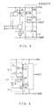
- FIG. 1 is a circuit diagram of a TTL type NAND gate circuit.
- the base electrode of an NPN type Schottky barrier bipolar transistor (hereafter called an "S bipolar transistor") Q1 is connected to an input terminal A via a diode D1 and, at the same time, is connected to another input terminal B via a diode D2 .
- the conductivity of the S bipolar transistor Q1 is controlled according to the input signals applied to the input terminals A and B .
- the base electrode of an NPN bipolar transistor Q2 is connected to the emitter electrode of the S bipolar transistor Q1 .
- the conductivity of the S bipolar transistor Q2 is controlled by the S bipolar transistor Q1 .
- a resistor R1 is inserted between the collector electrode of the S bipolar transistor Q2 and a voltage source terminal Vcc .
- the current flowing in the resistor R1 is controlled by the S bipolar transistor Q2 .
- the base electrode of an NPN type S bipolar transistor Q3 is connected to the collector electrode of the S bipolar transistor Q2 .
- the emitter electrode of an NPN bipolar transistor Q4 which is in a Darlington-connection with the S bipolar transistor Q3 , is connected to an output terminal OUT .
- the bipolar transistor Q4 and an NPN type S bipolar transistor Q5 are connected in totem-pole configuration between the voltage source terminal Vcc and the ground terminal GND .
- the collector electrode of the S bipolar transistor Q5 is connected to the output terminal OUT .
- the conductivity of the bipolar transistor Q4 and the S bipolar transistor Q5 is controlled by the S bipolar transistor Q2 .
- the base current of the S bipolar transistor Q3 is regulated by the resistor R1 .
- the base electrode of the bipolar transistor Q4 and the output terminal OUT are respectively connected to the collector electrode of the S bipolar transistor Q2 via corresponding Schottky barrier diodes D3 and D4 .
- the base potential of the S bipolar transistor Q3 rises, as shown by a in FIG. 2 .
- Vbe base to emitter voltage
- the S bipolar transistor Q3 and the bipolar transistor Q4 changes into the conductive state and an output signal with a steep rise is outputted from the output terminal OUT , as shown by b in FIG. 2 .
- the rising rate of the base potential of the S bipolar transistor Q3 depends on the resistance value of the resistor R1 .
- the rising of the output signal also depends on the resistance value of the resistor R1 .
- an object of this invention is to provide a logic circuit which is capable of high speed operation with low power consumption
- Another object of this invention is to provide a logic circuit in which the wave form of the output can be modified voluntarily.
- this invention provides a logic circuit for supplying an output signal having a prescribed waveform and one of two levels in response to a prescribed input signal and a power source voltage, which comprises: output circuit means for generating the output signal, including first and second output transistor means for alternately providing a first level output signal and a second level output signal; resistive means responsive to the power source voltage for supplying a current to the first output transistor means; current control means connected in parallel with the resistive means for controlling the current supplied to the first output transistor means, including first and second MOS transistor means for controlling the waveform of the first level output signal in accordance with the ratio of the channel length to the width of the first and second MOS transistor means; and output control means for controlling the first and second output transistor means in response to the input signal for supplying one of the first level output signal and the second level output signal.
- the circuit of this invention a large current is supplied to the output circuit means when the output signal changes from a low level to a high level. Therefore, the high rising rate, namely the high speed operation is obtained.
- the current control means operates to supply a small current to the output circuit means. Therefore, the power consumption is reduced.
- FIG. 3 is a schematic block diagram of a logic circuit of an embodiment of this invention.
- the logic circuit shown in FIG. 3 executes logic operations on input signals applied to input terminals A and B.
- This logic circuit comprises an output unit 1, an output control circuit 3, a current control unit 5, a resistor R1 and a discharge unit 7.
- the output unit 1 supplies the logic operation results to an output terminal OUT.
- the output control unit 3 receives the input signals and controls the output unit 1.
- the current control unit 5 controls the current supplied to the output unit 1 according to the input signals.
- the output unit 1 is provided with a first output section 11 including a Darlington-connected NPN type S bipolar transistor Q10 and a bipolar transistor Q11 , and a second output section 12 including an S bipolar transistor Q12 which is connected to the bipolar transistor Q11 in totem-pole form.
- the connection of the emitter electrode of the transistor Q11 and the collector electrode of the S transistor Q12 is connected to the output terminal OUT .
- the base electrodes of the S bipolar transistor Q10 and Q12 are connected to a first node n1 and a second node n2 , respectively.
- the first node n1 is connected to the voltage source terminal Vcc via the resistor R1 .
- the collector electrode of the transistor Q10 is connected to the voltage source terminal Vcc via a resistor R2 .
- the emitter electrode of the transistor Q10 is connected to the output terminal OUT via a resistor R3 .
- the output control unit 3 is inserted between the first node n1 and the second node n2 , and controls the conductivity of the S bipolar transistors Q10 and Q12 in the output unit 1 , according to the input signals supplied to the input terminals A and B .
- the current control unit 5 is connected in parallel with the resistor R1 and controls the base current of the S bipolar transistor Q10 by changing the impedance between the base electrode of the S bipolar transistor Q10 and the voltage source terminal Vcc according to the input signals and the base potential of the S bipolar transistor Q10 .
- the base potential of the S bipolar transistor Q10 is 2.Vbe higher than the output level, the potential at the first node n1 depends on the output signal level.
- the discharge unit 7 is connected between the second node n2 and the ground terminal GND .
- the discharge unit 7 discharges the base charge of the S transistor Q12 to change the S transistor Q12 from a conductive state to an non-conductive state, and prevents a through current flowing from the voltage source terminal Vcc to the ground terminal GND via the bipolar transistor Q11 and the S bipolar transistor Q12 during the switching operation of the output unit 1 .
- the current control unit 5 when the output signal rises from a low level to a high level, namely during the base potential of the S bipolar transistor Q10 is below a predetermined level, the current control unit 5 has a specified impedance.
- a parallel connection of the resistor R1 and the current control unit 5 is formed between the voltage source terminal Vcc and the first node n1 . Therefore, a larger current is applied to the S bipolar transistor Q10 than in the case when the impedance between voltage source terminal Vcc and the S bipolar transistor Q10 is only the resistance of the resistor R1 .
- the S bipolar transistor Q10 and the bipolar transistor Q11 change into the conducting state quickly, and so the output signal rises from a low level to a high level very fast.
- the current control unit 5 changes into an open state.
- the voltage source terminal Vcc and the base electrode of the S bipolar transistor Q10 are connected only via the resistor R1 . Therefore, the impedance between the voltage source terminal Vcc and the first node n1 increases.
- the base current of the S bipolar transistor Q10 decreases in comparison with the case when the first node n1 is connected to the voltage source terminal Vcc via the parallel circuit of the resistor R1 and the current control unit 5 . Therefore, when the output signal has become in the high level state and the circuit has become in the static state, the base current of the S bipolar transistor Q10 decreases.
- FIG. 4 is a circuit diagram of a logic circuit constitutes an inverter circuit according to this invention.
- an output control unit 3 comprises an N -channel MOS transistor (hereafter called “ NMOS ”) N1 .
- a current control unit 5 is composed of a P -channel MOS transistors (hereafter called “ PMOS ”) P1 and P2 .
- a discharge unit 7 is composed of an NMOS N2 and an inverter 9.
- An output unit 1 is of the same composition as in FIG. 3 .
- the NMOS N1 is connected between the first node n1 and the second node n2 , and the gate electrode thereof is connected to an input terminal A to which the input signal is applied.
- the NMOS N2 is connected between the second node n2 and the ground terminal GND , and the gate electrode thereof is connected to the input terminal A via the inverter 9 .
- the PMOS P1 and P2 are connected in series, and are inserted between the voltage source terminal Vcc and the first node n1 .
- the gate electrode of the PMOS P1 is connected to the first node n1 , and the gate electrode of the PMOS P2 is connected to the input terminal A .
- the S bipolar transistor Q12 when the input signal is in the high level, the PMOS P2 and the NMOS N2 are in the non-conducting state, and the NMOS N1 is in the conducting state, respectively.
- the S bipolar transistor Q12 the base electrode thereof is connected to the second node n2 , is supplied with the base current from the voltage source terminal Vcc via the resistor R1 and the NMOS N1 . Therefore, the S bipolar transistor Q12 is in the conducting state, and the output signal is in a low level.
- the S bipolar transistor Q10 is in the non-conducting state, and the PMOS P1 is supplied with a low level potential at the gate electrode thereof.
- the NMOS N1 changes into the non-conducting state
- the PMOS P1 and P2 change into the conducting state, respectively.
- the switching operation of the S bipolar transistor Q10 is performed at high speed, and thus the rising of the output signal from a low level to a high level can be carried out at high speed.
- the ON resistance of the M0S transistors is determined by the length and the width of the channel region thereof, it is possible to vary the impedance of the current control unit 5 .
- the impedance of the current control unit 5 it is possible to vary or modify the wave form of the output signal voluntary. Namely, the rising of the output is steep, a high frequency noise is easily occured. Thus, when such noise is unfavorable, it is possible to make the rising gentle by changing the impedance of the current control unit 5 .
- the PMOS P1 In the static state, when the output signal and the potential at the first node n1 are in the high level, the PMOS P1 is in the non-conducting state. Thus, the current to the base electrode of the S transistor Q10 is supplied via the resistor R1 alone. Therefore, the operating current decreases compared with the case when the parallel connection of the resistor R1 and the PMOS P1 and P2 is formed.
- FIG.5 is a diagram illustrating a simulation results of the characteristic curves of the prior art and the circuit of FIG.4 .
- the curve i shows the characteristic of this invention
- the curve f shows the characteristic of the prior art.
- the operating current in the low frequency band can be reduced to about half that of prior art, according to this invention.
- FIG. 6 is a circuit diagram of another embodiment of this invention of a logic circuit which constitutes an inverter circuit.
- This logic circuit comprises a Schottkey barrier diode D5 inserted between the drain electrode of the PMOS P2 and the drain electrode of the NMOS N1 , but the remainder of the composition is the same as in the logic circuit shown in FIG.4 .
- the diode D5 prevents a charging current from the voltage source terminal Vcc to the parasitic capacitance, which exists at the node of the PMOS P1 and the PMOS P2 , via the resistor R1 and the PMOS P2 when the PMOS P1 changes into the non-conducting state. For this reason, the delay of the rising time of the base potential of the S bipolar transistor Q10 can be prevented. Thus, a high speed operation is obtained.
- FIG.7 is a circuit diagram of a further embodiment of this invention of a logic circuit which constitutes a 2-input NOR gate circuit.
- the output unit 1 is the same as shown in FIG.3 .
- An output control unit 3 comprises an NMOS N3 , whose gate electrode is connected to the input terminal A , and an NM0S N4 , whose gate electrode is connected to an input terminal B .
- the NMOS N3 and the N4 are connected in parallel between the first node n1 and the second node n2 .
- a current control unit 5 comprises PMOS P3 and P4 , whose gate electrodes are connected respectively to the corresponding input terminals A and B .
- a diode D5 is connected between the PMOS P4 and the NMOS N4 .
- a discharge unit 7 is constructed by a resistor R4 .
- the impedance between the first node n1 and the voltage source terminal Vcc varies according to the input signal, even though it is a 2-input NOR circuit.
- the same kind of effect namely a high speed operation and a low power consumption, is obtained.
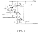
- the output control unit 3 and the current control unit 5 it is possible to make the logic circuit function as a NAND circuit.
- FIG.8 is an example of an NAND circuit.
- an output control circuit 3 comprises NMOS N3 and N4 , whose gate electrodes are connected to input terminals A and B , respectively.
- An current control circuit 5 comprises PMOS P1 , P3 and P4 , and a Schottky barrier diode D5 .
- the PMOS P3 and P4 are connected in parallel, and the gate electrodes thereof are connected to the input terminals A and B , respectively.
- the output signal level is low, namely the potential at the first node n1 is in low level
- the PMOS P3 or P4 changes into conductive state in responsive to a low level input signal.
- the output control unit 3 is composed of MOS type transistors.
- the invention is not limited to this and, for example, a bipolar transistor may be used.
- the discharge unit 7 is not limited to a MOS transistor or a resistor and, naturally, any other type of construction may be used.
Landscapes
- Physics & Mathematics (AREA)
- Engineering & Computer Science (AREA)
- Computer Hardware Design (AREA)
- Computing Systems (AREA)
- General Engineering & Computer Science (AREA)
- Mathematical Physics (AREA)
- Logic Circuits (AREA)
- Electronic Switches (AREA)
Applications Claiming Priority (2)
| Application Number | Priority Date | Filing Date | Title |
|---|---|---|---|
| JP62194527A JPH0666681B2 (ja) | 1987-08-05 | 1987-08-05 | 論理回路 |
| JP194527/87 | 1987-08-05 |
Publications (3)
| Publication Number | Publication Date |
|---|---|
| EP0302671A2 true EP0302671A2 (fr) | 1989-02-08 |
| EP0302671A3 EP0302671A3 (en) | 1990-02-07 |
| EP0302671B1 EP0302671B1 (fr) | 1993-10-06 |
Family
ID=16326016
Family Applications (1)
| Application Number | Title | Priority Date | Filing Date |
|---|---|---|---|
| EP88307022A Expired - Lifetime EP0302671B1 (fr) | 1987-08-05 | 1988-07-29 | Circuit logique |
Country Status (5)
| Country | Link |
|---|---|
| US (1) | US4841172A (fr) |
| EP (1) | EP0302671B1 (fr) |
| JP (1) | JPH0666681B2 (fr) |
| KR (1) | KR910005588B1 (fr) |
| DE (1) | DE3884713T2 (fr) |
Families Citing this family (6)
| Publication number | Priority date | Publication date | Assignee | Title |
|---|---|---|---|---|
| JP2619415B2 (ja) * | 1987-09-24 | 1997-06-11 | 株式会社日立製作所 | 半導体論理回路 |
| NL8800234A (nl) * | 1988-02-01 | 1989-09-01 | Philips Nv | Geintegreerde schakeling met logische circuits en ten minste een push-pull-trap. |
| US4897564A (en) * | 1988-12-27 | 1990-01-30 | International Business Machines Corp. | BICMOS driver circuit for high density CMOS logic circuits |
| JPH0736507B2 (ja) * | 1989-02-02 | 1995-04-19 | 株式会社東芝 | 半導体論理回路 |
| US5343092A (en) * | 1992-04-27 | 1994-08-30 | International Business Machines Corporation | Self-biased feedback-controlled active pull-down signal switching |
| US6294959B1 (en) | 1999-11-12 | 2001-09-25 | Macmillan Bruce E. | Circuit that operates in a manner substantially complementary to an amplifying device included therein and apparatus incorporating same |
Family Cites Families (9)
| Publication number | Priority date | Publication date | Assignee | Title |
|---|---|---|---|---|
| JPS53116768A (en) * | 1977-03-22 | 1978-10-12 | Nec Corp | Logical operation circuit |
| US4430585A (en) * | 1981-12-30 | 1984-02-07 | Bell Telephone Laboratories, Incorporated | Tristate transistor logic circuit with reduced power dissipation |
| JPS6066519A (ja) * | 1983-09-22 | 1985-04-16 | Nec Corp | 半導体論理回路 |
| US4623803A (en) * | 1983-11-08 | 1986-11-18 | Advanced Micro Devices, Inc. | Logic level translator circuit for integrated circuit semiconductor devices having transistor-transistor logic output circuitry |
| FR2561472B1 (fr) * | 1984-03-19 | 1991-05-10 | Cit Alcatel | Translateur de niveaux logiques |
| JPS6184112A (ja) * | 1984-10-02 | 1986-04-28 | Fujitsu Ltd | 論理ゲ−ト回路 |
| DE3580267D1 (de) * | 1985-01-15 | 1990-11-29 | Texas Instruments Inc | Einstellbare beschleunigungsschaltung fuer gatter des ttl-typs. |
| US4737665A (en) * | 1985-01-15 | 1988-04-12 | Texas Instruments Incorporated | Adjustable speed up circuit for TTL-type gates |
| US4746817A (en) * | 1987-03-16 | 1988-05-24 | International Business Machines Corporation | BIFET logic circuit |
-
1987
- 1987-08-05 JP JP62194527A patent/JPH0666681B2/ja not_active Expired - Lifetime
-
1988
- 1988-07-28 US US07/225,495 patent/US4841172A/en not_active Expired - Lifetime
- 1988-07-29 EP EP88307022A patent/EP0302671B1/fr not_active Expired - Lifetime
- 1988-07-29 DE DE88307022T patent/DE3884713T2/de not_active Expired - Lifetime
- 1988-08-05 KR KR1019880009991A patent/KR910005588B1/ko not_active Expired
Also Published As
| Publication number | Publication date |
|---|---|
| US4841172A (en) | 1989-06-20 |
| EP0302671A3 (en) | 1990-02-07 |
| KR890004498A (ko) | 1989-04-22 |
| DE3884713D1 (de) | 1993-11-11 |
| KR910005588B1 (ko) | 1991-07-31 |
| DE3884713T2 (de) | 1994-03-10 |
| EP0302671B1 (fr) | 1993-10-06 |
| JPH0666681B2 (ja) | 1994-08-24 |
| JPS6439821A (en) | 1989-02-10 |
Similar Documents
| Publication | Publication Date | Title |
|---|---|---|
| US6624672B2 (en) | Output buffer with constant switching current | |
| KR0136775B1 (ko) | 스위칭 유도 잡음을 감소시키는 출력 버퍼 | |
| US6094104A (en) | Voltage and temperature compensated ring oscillator frequency stabilizer | |
| US6407594B1 (en) | Zero bias current driver control circuit | |
| US4703199A (en) | Non-restricted level shifter | |
| EP0279332A1 (fr) | Circuit logique utilisé dans des circuits intégrés standard à niveau de logique CMOS | |
| EP0231667A2 (fr) | Circuits de tampon de sortie | |
| US5250854A (en) | Bitline pull-up circuit operable in a low-resistance test mode | |
| EP0230306B1 (fr) | Circuit trigger de Schmitt | |
| US5003199A (en) | Emitter coupled logic circuit having an active pull-down output stage | |
| JPH0693615B2 (ja) | ドライバ回路 | |
| KR900000487B1 (ko) | 논리 게이트 회로 | |
| JPH07202665A (ja) | ドライバ/レシーバ回路 | |
| KR930001439B1 (ko) | BiCMOS용 출력회로 | |
| KR910009083B1 (ko) | 반도체장치의 출력회로 | |
| EP0302671B1 (fr) | Circuit logique | |
| JP2743401B2 (ja) | Ecl回路 | |
| US5254885A (en) | Bi-CMOS logic circuit with feedback | |
| KR970006874B1 (ko) | 달링톤 BiCMOS 구동기 회로 | |
| US4535258A (en) | Transistor-transistor logic circuit with improved switching times | |
| JP3426337B2 (ja) | 零バイアス電流ローサイドドライバーコントロール回路 | |
| EP0432472A2 (fr) | Circuit CMOS comportant des transistors bipolaires dans l'étage de sortie | |
| EP0125733A1 (fr) | Circuit utilisant des transistors à effet de champ complémentaires à perte isolée | |
| EP0645890A2 (fr) | Circuit logique BICMOS | |
| KR930007560B1 (ko) | 출력회로 |
Legal Events
| Date | Code | Title | Description |
|---|---|---|---|
| PUAI | Public reference made under article 153(3) epc to a published international application that has entered the european phase |
Free format text: ORIGINAL CODE: 0009012 |
|
| 17P | Request for examination filed |
Effective date: 19880817 |
|
| AK | Designated contracting states |
Kind code of ref document: A2 Designated state(s): DE FR GB |
|
| PUAL | Search report despatched |
Free format text: ORIGINAL CODE: 0009013 |
|
| AK | Designated contracting states |
Kind code of ref document: A3 Designated state(s): DE FR GB |
|
| 17Q | First examination report despatched |
Effective date: 19920102 |
|
| GRAA | (expected) grant |
Free format text: ORIGINAL CODE: 0009210 |
|
| AK | Designated contracting states |
Kind code of ref document: B1 Designated state(s): DE FR GB |
|
| REF | Corresponds to: |
Ref document number: 3884713 Country of ref document: DE Date of ref document: 19931111 |
|
| ET | Fr: translation filed | ||
| PLBE | No opposition filed within time limit |
Free format text: ORIGINAL CODE: 0009261 |
|
| STAA | Information on the status of an ep patent application or granted ep patent |
Free format text: STATUS: NO OPPOSITION FILED WITHIN TIME LIMIT |
|
| 26N | No opposition filed | ||
| REG | Reference to a national code |
Ref country code: GB Ref legal event code: 746 Effective date: 19981015 |
|
| REG | Reference to a national code |
Ref country code: FR Ref legal event code: D6 |
|
| REG | Reference to a national code |
Ref country code: GB Ref legal event code: IF02 |
|
| PGFP | Annual fee paid to national office [announced via postgrant information from national office to epo] |
Ref country code: DE Payment date: 20070726 Year of fee payment: 20 |
|
| PGFP | Annual fee paid to national office [announced via postgrant information from national office to epo] |
Ref country code: GB Payment date: 20070725 Year of fee payment: 20 |
|
| PGFP | Annual fee paid to national office [announced via postgrant information from national office to epo] |
Ref country code: FR Payment date: 20070710 Year of fee payment: 20 |
|
| REG | Reference to a national code |
Ref country code: GB Ref legal event code: PE20 Expiry date: 20080728 |
|
| PG25 | Lapsed in a contracting state [announced via postgrant information from national office to epo] |
Ref country code: GB Free format text: LAPSE BECAUSE OF EXPIRATION OF PROTECTION Effective date: 20080728 |