EP0304896A2 - Dispositif de mémoire non volatile à semi-conducteur et méthode de fabrication - Google Patents
Dispositif de mémoire non volatile à semi-conducteur et méthode de fabrication Download PDFInfo
- Publication number
- EP0304896A2 EP0304896A2 EP88113799A EP88113799A EP0304896A2 EP 0304896 A2 EP0304896 A2 EP 0304896A2 EP 88113799 A EP88113799 A EP 88113799A EP 88113799 A EP88113799 A EP 88113799A EP 0304896 A2 EP0304896 A2 EP 0304896A2
- Authority
- EP
- European Patent Office
- Prior art keywords
- layer
- groove
- region
- silicon dioxide
- memory device
- Prior art date
- Legal status (The legal status is an assumption and is not a legal conclusion. Google has not performed a legal analysis and makes no representation as to the accuracy of the status listed.)
- Granted
Links
- 239000004065 semiconductor Substances 0.000 title claims description 75
- 238000000034 method Methods 0.000 title claims description 23
- 238000004519 manufacturing process Methods 0.000 title claims description 7
- VYPSYNLAJGMNEJ-UHFFFAOYSA-N Silicium dioxide Chemical compound O=[Si]=O VYPSYNLAJGMNEJ-UHFFFAOYSA-N 0.000 claims abstract description 138
- 235000012239 silicon dioxide Nutrition 0.000 claims abstract description 69
- 239000000377 silicon dioxide Substances 0.000 claims abstract description 69
- 229910021420 polycrystalline silicon Inorganic materials 0.000 claims abstract description 68
- 229920005591 polysilicon Polymers 0.000 claims abstract description 63
- 238000005530 etching Methods 0.000 claims description 24
- 239000012535 impurity Substances 0.000 claims description 19
- 238000000926 separation method Methods 0.000 claims description 18
- 229910052581 Si3N4 Inorganic materials 0.000 claims description 16
- HQVNEWCFYHHQES-UHFFFAOYSA-N silicon nitride Chemical compound N12[Si]34N5[Si]62N3[Si]51N64 HQVNEWCFYHHQES-UHFFFAOYSA-N 0.000 claims description 16
- 238000007254 oxidation reaction Methods 0.000 claims description 8
- 238000000151 deposition Methods 0.000 claims description 4
- 238000010438 heat treatment Methods 0.000 claims description 4
- 239000003870 refractory metal Substances 0.000 claims description 3
- 229910021332 silicide Inorganic materials 0.000 claims description 3
- FVBUAEGBCNSCDD-UHFFFAOYSA-N silicide(4-) Chemical compound [Si-4] FVBUAEGBCNSCDD-UHFFFAOYSA-N 0.000 claims description 3
- 238000009792 diffusion process Methods 0.000 abstract description 12
- 229960001866 silicon dioxide Drugs 0.000 description 55
- 239000000758 substrate Substances 0.000 description 8
- 229910052710 silicon Inorganic materials 0.000 description 6
- XUIMIQQOPSSXEZ-UHFFFAOYSA-N Silicon Chemical compound [Si] XUIMIQQOPSSXEZ-UHFFFAOYSA-N 0.000 description 4
- 229910052751 metal Inorganic materials 0.000 description 4
- 239000002184 metal Substances 0.000 description 4
- 230000003647 oxidation Effects 0.000 description 4
- 238000001020 plasma etching Methods 0.000 description 4
- 239000010703 silicon Substances 0.000 description 4
- 229920002120 photoresistant polymer Polymers 0.000 description 3
- ZOXJGFHDIHLPTG-UHFFFAOYSA-N Boron Chemical compound [B] ZOXJGFHDIHLPTG-UHFFFAOYSA-N 0.000 description 2
- OAICVXFJPJFONN-UHFFFAOYSA-N Phosphorus Chemical compound [P] OAICVXFJPJFONN-UHFFFAOYSA-N 0.000 description 2
- 229910052782 aluminium Inorganic materials 0.000 description 2
- 229910052796 boron Inorganic materials 0.000 description 2
- 229910052802 copper Inorganic materials 0.000 description 2
- 239000002784 hot electron Substances 0.000 description 2
- BHEPBYXIRTUNPN-UHFFFAOYSA-N hydridophosphorus(.) (triplet) Chemical compound [PH] BHEPBYXIRTUNPN-UHFFFAOYSA-N 0.000 description 2
- 238000009413 insulation Methods 0.000 description 2
- 238000002161 passivation Methods 0.000 description 2
- 229910052698 phosphorus Inorganic materials 0.000 description 2
- 239000011574 phosphorus Substances 0.000 description 2
- ZOKXTWBITQBERF-UHFFFAOYSA-N Molybdenum Chemical compound [Mo] ZOKXTWBITQBERF-UHFFFAOYSA-N 0.000 description 1
- 101100521334 Mus musculus Prom1 gene Proteins 0.000 description 1
- RTAQQCXQSZGOHL-UHFFFAOYSA-N Titanium Chemical compound [Ti] RTAQQCXQSZGOHL-UHFFFAOYSA-N 0.000 description 1
- 229910045601 alloy Inorganic materials 0.000 description 1
- 239000000956 alloy Substances 0.000 description 1
- 230000015572 biosynthetic process Effects 0.000 description 1
- 230000003247 decreasing effect Effects 0.000 description 1
- 230000000593 degrading effect Effects 0.000 description 1
- 150000002500 ions Chemical class 0.000 description 1
- 230000000873 masking effect Effects 0.000 description 1
- 229910052750 molybdenum Inorganic materials 0.000 description 1
- 239000011733 molybdenum Substances 0.000 description 1
- 230000001590 oxidative effect Effects 0.000 description 1
- 238000000059 patterning Methods 0.000 description 1
- 229910052719 titanium Inorganic materials 0.000 description 1
- 239000010936 titanium Substances 0.000 description 1
- WFKWXMTUELFFGS-UHFFFAOYSA-N tungsten Chemical compound [W] WFKWXMTUELFFGS-UHFFFAOYSA-N 0.000 description 1
- 229910052721 tungsten Inorganic materials 0.000 description 1
- 239000010937 tungsten Substances 0.000 description 1
- 238000001039 wet etching Methods 0.000 description 1
Images


Classifications
-
- H—ELECTRICITY
- H10—SEMICONDUCTOR DEVICES; ELECTRIC SOLID-STATE DEVICES NOT OTHERWISE PROVIDED FOR
- H10B—ELECTRONIC MEMORY DEVICES
- H10B41/00—Electrically erasable-and-programmable ROM [EEPROM] devices comprising floating gates
-
- H—ELECTRICITY
- H10—SEMICONDUCTOR DEVICES; ELECTRIC SOLID-STATE DEVICES NOT OTHERWISE PROVIDED FOR
- H10B—ELECTRONIC MEMORY DEVICES
- H10B69/00—Erasable-and-programmable ROM [EPROM] devices not provided for in groups H10B41/00 - H10B63/00, e.g. ultraviolet erasable-and-programmable ROM [UVEPROM] devices
-
- H—ELECTRICITY
- H10—SEMICONDUCTOR DEVICES; ELECTRIC SOLID-STATE DEVICES NOT OTHERWISE PROVIDED FOR
- H10D—INORGANIC ELECTRIC SEMICONDUCTOR DEVICES
- H10D30/00—Field-effect transistors [FET]
- H10D30/01—Manufacture or treatment
- H10D30/021—Manufacture or treatment of FETs having insulated gates [IGFET]
- H10D30/0411—Manufacture or treatment of FETs having insulated gates [IGFET] of FETs having floating gates
-
- H—ELECTRICITY
- H10—SEMICONDUCTOR DEVICES; ELECTRIC SOLID-STATE DEVICES NOT OTHERWISE PROVIDED FOR
- H10D—INORGANIC ELECTRIC SEMICONDUCTOR DEVICES
- H10D30/00—Field-effect transistors [FET]
- H10D30/60—Insulated-gate field-effect transistors [IGFET]
- H10D30/68—Floating-gate IGFETs
- H10D30/681—Floating-gate IGFETs having only two programming levels
- H10D30/684—Floating-gate IGFETs having only two programming levels programmed by hot carrier injection
- H10D30/685—Floating-gate IGFETs having only two programming levels programmed by hot carrier injection from the channel
-
- H—ELECTRICITY
- H10—SEMICONDUCTOR DEVICES; ELECTRIC SOLID-STATE DEVICES NOT OTHERWISE PROVIDED FOR
- H10D—INORGANIC ELECTRIC SEMICONDUCTOR DEVICES
- H10D64/00—Electrodes of devices having potential barriers
- H10D64/01—Manufacture or treatment
- H10D64/031—Manufacture or treatment of data-storage electrodes
- H10D64/035—Manufacture or treatment of data-storage electrodes comprising conductor-insulator-conductor-insulator-semiconductor structures
Definitions
- the present invention relates to a non-volatile semiconductor memory device and a method of manufacture thereof.
- Memory cells used in a programmable read only memory (PROM), one type of non-volatile semiconductor memory device, are each formed of a non-volatile transistor for storing data and a transistor for selecting the memory cell.
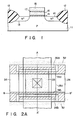
- Fig. 1 illustrates a sectional view of a non-volatile transistor used in memory cells of a conventional PROM.
- a field oxide layer 12 is formed over the surface of a P-type silicon substrate 11.
- An N+-type source region 13 and an N+-type drain region 14 are formed in the substrate to be surrounded by a field oxide layer 12.
- a first gate insulation layer 15, a floating gate electrode 16 of polysilicon, a second gate insulation layer 17 and a control gate electrode 18 of polysilicon are sequentially formed over a portion of the substrate between source region 13 and drain region 14.
- the PROM To construct the PROM, a great number of non-volatile transistors as described above must be formed on the substrate. And, to realize a large-capacity memory, the dimensions of the non-volatile transistor in the longitudinal and horizontal directions thereof should be made very small. However, in conventional PROMs using non-volatile transistors having such a structure as shown in Fig. 1, simply decreasing the dimensions of each non-volatile transistor on a plane would degrade reliability and separation characteristics of transistors.
- a non-volatile memory device comprising: a first semiconductor region of a first conductivity type; a groove formed in said first semiconductor region to extend in a predetermined direction; insulating separation regions formed to selectively fill the inside of said groove; a second semiconductor region of a second conductivity type formed in a surface of said first semiconductor region and serving as a source or drain region; a first gate insulating layer formed on a side wall of a groove portion defined by said insulating separation regions and said first semiconductor region, said side wall being along the direction of extension of said groove; a floating gate electrode formed on a surface of said gate first insulating layer opposite to a surface thereof contacting said side wall of said groove portion; a second gate insulating layer formed on a surface of said floating gate electrode opposite to a surface thereof contacting said first gate insulating layer; a control gate electrode formed on a surface of said second gate insulating layer opposite to a surface thereof
- a method of manufacturing a non-volatile memory device comprising the steps of: adding to a surface of a first semiconductor region of a first conductivity type impurities of a second type conductivity type to form a second semiconductor region; forming a groove in said first semiconductor region to extend in a predetermined direction by an anisotropic etching technique using a predetermined mask; filling said groove with an insulating separation layer; selectively removing said insulating separation layer by an isotropic etching technique using a predetermined mask to separate said groove into a plurality of groove portions; sequentially forming a first silicon dioxide layer, a first polysilicon layer, a second silicon dioxide layer and a silicon nitride layer over an entire surface including inside surfaces of said groove portion defined by said insulating separation layer and said first semiconductor region; selectively etching said first silicon dioxide layer, said first polysilicon layer, said second silicon dioxide layer and said silicon nitrid
- a non-volatile transistor is formed ver strictlytically by forming a floating gate electrode and a control gate electrode of a non-volatile transistor on a side wall of a groove formed in a first semiconductor region, forming a source or drain region of the transistor in a surface of the first semiconductor region, and forming a drain or source region of the transistor at the bottom of the groove.
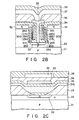
- Fig. 2A is a plan view or pattern layout showing a structure of a transistor used in a non-volatile semiconductor device according to the present invention
- Fig. 2B is a sectional view taken along A-A′ line of Fig. 2A
- Fig. 2C is a sectional view taken along B-B′ line of Fig. 2A.
- a P-well region 22 is formed on a P-type silicon substrate 21.
- a groove 23 is formed to extend in a predetermined direction as shown in Fig. 3.
- the side walls of groove 23 are formed perpendicular to the surface of P-well region 22.
- a silicon dioxide layer 24 is selectively embeded in groove 23 as shown in Fig. 4.
- groove 23 is separated into a plurality of portions 23a by silicon dioxide layer 24 and P-well region 22.
- the lower portion of silicon dioxide layer 24 embeded in groove 23 is slanted along the direction of extension of groove 23 by an angle ⁇ below 45 degrees.
- Silicon dioxide layers 25a and 25b used as first gate insulating layers are formed on side walls of groove portion 23a which are faced each other in the direction normal to the direction of extension of groove 23.
- Phosphorus-doped polysilicon layers 26a and 26b are provided on silicon dioxide layers 25a and 25b, respectively.
- a second gate insulating layer 30a (30b) which is comprised of three layers of a silicon dioxide layer 27a (27b), a silicon nitride layer 28a (28b) and a silicon dioxide layer 29a (29b).
- Phosphorus-doped polysilicon layers 31a and 31b are formed on second gate insulating layers 30a and 30b, respectively. As shown in Fig. 2A, polysilicon layers 31a and 31b are each formed to extend from groove portion 23a so that they are common to groove portion 23a and other groove portions adjacent thereto.
- a silicon dioxide layer 34 is deposited over the entire surface of P well region 22 involving the inside of groove portion 23. An opening is formed in silicon dioxide layer 34 which reaches the surface of N-type diffusion layer 33, and a polysilicon layer 35 is formed in the opening. Polysilicon layer 35 has a low resistivity because of introduction thereto of impurities at a sufficiently high concentration. Further, a silicon dioxide layer 36 is deposited on silicon dioxide layer 34 and polysilicon layer 35. An opening is formed in silicon dioxide layer 36 which reaches the surface of polysilicon layer 35, and a metal layer 37 made of Al, Si and Cu is formed in the opening. Further, a passivation layer 38 formed of PSG, SiN or the like is deposited over metal layer 37.
- two non-volatile transistors are formed within each of groove portions 23a. And, the source region and the drain region of each transistor are separated in the direction of depth of groove portion 23a so that there is little possibility of occurrence of leak current due to scale-down of the dimensions of transistors in two dimensions. Since two transistors are formed within each of groove portions 23a, a considerable reduction in the size of transistors will be made possible. For instance, when the same design rules are applied, the size of a cell will be reduced to about 70% of the size of a cell used in a conventional memory.
- N-type diffusion regions 32 are provided on the top of the memory cell, there is no need of allowance for the formation of device-separating regions.
- polysilicon layers 26a and 26b serving as the floating gate electrodes and polysilicon layers serving as the control gate electrodes are doped with phosphorus acting as N-type impurities.
- these polysilicon layers may be doped with boron of P-type impurities.
- P well region 22 is formed over the entire surface of P-type silicon substrate 21 to a thickness of about 4.5 ⁇ m.
- groove 23 of approximate depth 1.2 ⁇ m and approximate width 1.2 ⁇ m is vertically formed in P well region 22 by RIE (reactive ion etching) technique using a proper mask. It is to be noted that in Fig. 5B groove 23 is drawn larger than its actual size, and formed to extend in a predetermined direction as shown in Fig. 3.
- silicon dioxide layer 24 is deposited over the entire surface to a thickness of about 7000 ⁇ so that groove 23 is filled. Further, a photoresist layer 41 is deposited on silicon dioxide layer 24 to planalize the top surface of the device.
- photoresist layer 41 and silicon dioxide layer 24 are etched away to leave silicon dioxide layer 24 only within groove 23 as shown in Fig. 5D.
- silicon dioxide layer 25 is formed over the entire surface including the inside surface of groove portion 23a at a thickness of 200 ⁇ , and polysilicon layer 26 doped with phosphorus is deposited by CVD on silicon dioxide layer 25 to a thickness of 1000 ⁇ .
- silicon dioxide layer 27 of a thickness of 100 ⁇ is formed on polysilicon layer 26 by thermal oxidation, and silicon nitride layer 28 is further deposited by CVD, at a thickness of 100 ⁇ over silicon dioxide layer 27.
- silicon nitride layer 28, silicon dioxide layer 27, polysilicon layer 26 and silicon dioxide layer 25 remain only on side walls of groove portion 23a in the separate form of silicon nitride layers 28a and 28b; silicon dioxide layers 27a and 27b; polysilicon layers 26a and 26b; and silicon dioxide layers 25a and 25b. They are not left on the surface of silicon dioxide layer 24 shown in Fig. 4 and at the bottom of groove portion 23a.
- a silicon dioxide layer of a thickness of about 1000 ⁇ is formed only on exposed portions of polysilicon layers 26a and 26b, or the upper and lower ends thereof by heating oxidation at 900°C.
- thin silicon dioxide layers 29a and 29b have been formed on silicon nitride layers 28a and 28b.
- a Phosphorus-doped polysilicon layer of about 3000 ⁇ thickness is deposited over the entire surface by CVD, and the polysilicon layer is then patterned by an anisotropic etching technique, e.g., RIE technique using a mask of a predetermined shape.
- the patterning process leaves polysilicon layers 31a and 31b which are used as control electrodes of non-volatile transistors for memory cells, i.e., as a word line for memory cells.
- Silicon dioxide layer 27a, silicon nitride layer 28a and silicon dioxide layer 29a form second gate insulating layer 30a for one non-volatile transistor, while silicon dioxide layer 27b, silicon nitride layer 28b and silicon dioxide layer 29b form second gate insulating layer 30b for the other nonvolatile transistor.
- polysilicon layer 35 is deposited over the entire surface, and phosphorous is diffused at 1000°C from the top of polysilicon layer 35 to form N-type diffusion region 33 in the surface region of P well region 22 that is located at the bottom of groove portion 23a.
- silicon dioxide layer 36 is deposited by CVD over the entire surface to a thickness of 6000 ⁇ , and a contact hole is then formed in silicon dioxide layer 36 to expose the surface of polysilicon layer 35.
- a layer of an alloy of Al, Si and Cu is applied over the entire surface and patterned to form metal layer 37.
- passivation layer 38 formed of PSG or SiN is deposited over the entire surface, thereby completing the device.
- groove 23 is filled with silicon dioxide layer 24 deposited by CVD and then selectively etched away.
- groove 23 may be filled with a thermal oxide layer.
- control gate electrodes for non-volatile transistors are each formed of a polysilicon layer.
- two-layered control gate electrodes 53a and 53b may be used each of which is formed of a first layer 51a (51b) of polysilicon and a second layer 52a (52b) of a refractory metal silicide of molybdenum, tungsten, titanium or the like.
Landscapes
- Non-Volatile Memory (AREA)
- Semiconductor Memories (AREA)
Applications Claiming Priority (2)
| Application Number | Priority Date | Filing Date | Title |
|---|---|---|---|
| JP62210774A JP2735193B2 (ja) | 1987-08-25 | 1987-08-25 | 不揮発性半導体装置及びその製造方法 |
| JP210774/87 | 1987-08-25 |
Publications (3)
| Publication Number | Publication Date |
|---|---|
| EP0304896A2 true EP0304896A2 (fr) | 1989-03-01 |
| EP0304896A3 EP0304896A3 (en) | 1990-06-13 |
| EP0304896B1 EP0304896B1 (fr) | 1993-06-23 |
Family
ID=16594920
Family Applications (1)
| Application Number | Title | Priority Date | Filing Date |
|---|---|---|---|
| EP88113799A Expired - Lifetime EP0304896B1 (fr) | 1987-08-25 | 1988-08-24 | Dispositif de mémoire non volatile à semi-conducteur et méthode de fabrication |
Country Status (5)
| Country | Link |
|---|---|
| US (1) | US4929988A (fr) |
| EP (1) | EP0304896B1 (fr) |
| JP (1) | JP2735193B2 (fr) |
| KR (1) | KR920002091B1 (fr) |
| DE (1) | DE3881986T2 (fr) |
Cited By (3)
| Publication number | Priority date | Publication date | Assignee | Title |
|---|---|---|---|---|
| EP0430426A3 (en) * | 1989-11-01 | 1991-06-12 | American Telephone And Telegraph Company | Semiconductor memory device |
| US6724028B2 (en) | 2001-12-10 | 2004-04-20 | Hans Gude Gudesen | Matrix-addressable array of integrated transistor/memory structures |
| US7589372B2 (en) | 2004-08-13 | 2009-09-15 | Dongbu Electronics Co., Ltd. | Nonvolatile memory device and method for fabricating the same |
Families Citing this family (68)
| Publication number | Priority date | Publication date | Assignee | Title |
|---|---|---|---|---|
| US6081449A (en) * | 1987-05-12 | 2000-06-27 | Altera Corporation | High-density nonvolatile memory cell |
| JP2646563B2 (ja) * | 1987-07-15 | 1997-08-27 | ソニー株式会社 | 不揮発性メモリ装置 |
| JP2646591B2 (ja) * | 1987-11-27 | 1997-08-27 | ソニー株式会社 | 不揮発性メモリ装置 |
| JP2675572B2 (ja) * | 1988-03-31 | 1997-11-12 | 株式会社東芝 | 半導体集積回路の製造方法 |
| NL8900989A (nl) * | 1989-04-20 | 1990-11-16 | Philips Nv | Halfgeleiderinrichting met een in een kunststof omhulling ingebed halfgeleiderlichaam. |
| JPH02285638A (ja) * | 1989-04-27 | 1990-11-22 | Toshiba Corp | 半導体装置 |
| JPH07105453B2 (ja) * | 1989-07-13 | 1995-11-13 | 株式会社東芝 | 半導体記憶装置のセル構造 |
| US4964080A (en) * | 1990-03-09 | 1990-10-16 | Intel Corporation | Three-dimensional memory cell with integral select transistor |
| US5053842A (en) * | 1990-05-30 | 1991-10-01 | Seiko Instruments Inc. | Semiconductor nonvolatile memory |
| US5078498A (en) * | 1990-06-29 | 1992-01-07 | Texas Instruments Incorporated | Two-transistor programmable memory cell with a vertical floating gate transistor |
| US5041884A (en) * | 1990-10-11 | 1991-08-20 | Mitsubishi Denki Kabushiki Kaisha | Multilayer semiconductor integrated circuit |
| US5258634A (en) * | 1991-05-17 | 1993-11-02 | United Microelectronics Corporation | Electrically erasable read only memory cell array having elongated control gate in a trench |
| JPH0567791A (ja) * | 1991-06-20 | 1993-03-19 | Mitsubishi Electric Corp | 電気的に書込および消去可能な半導体記憶装置およびその製造方法 |
| JPH0613627A (ja) * | 1991-10-08 | 1994-01-21 | Semiconductor Energy Lab Co Ltd | 半導体装置およびその作製方法 |
| US5196722A (en) * | 1992-03-12 | 1993-03-23 | International Business Machines Corporation | Shadow ram cell having a shallow trench eeprom |
| US5399516A (en) * | 1992-03-12 | 1995-03-21 | International Business Machines Corporation | Method of making shadow RAM cell having a shallow trench EEPROM |
| US5467305A (en) * | 1992-03-12 | 1995-11-14 | International Business Machines Corporation | Three-dimensional direct-write EEPROM arrays and fabrication methods |
| US5315142A (en) * | 1992-03-23 | 1994-05-24 | International Business Machines Corporation | High performance trench EEPROM cell |
| JP2889061B2 (ja) * | 1992-09-25 | 1999-05-10 | ローム株式会社 | 半導体記憶装置およびその製法 |
| US5859455A (en) * | 1992-12-31 | 1999-01-12 | Yu; Shih-Chiang | Non-volatile semiconductor memory cell with control gate and floating gate and select gate located above the channel |
| US5460988A (en) * | 1994-04-25 | 1995-10-24 | United Microelectronics Corporation | Process for high density flash EPROM cell |
| US5670803A (en) * | 1995-02-08 | 1997-09-23 | International Business Machines Corporation | Three-dimensional SRAM trench structure and fabrication method therefor |
| US6965142B2 (en) * | 1995-03-07 | 2005-11-15 | Impinj, Inc. | Floating-gate semiconductor structures |
| US5945705A (en) * | 1995-08-01 | 1999-08-31 | Advanced Micro Devices, Inc. | Three-dimensional non-volatile memory |
| US5672524A (en) * | 1995-08-01 | 1997-09-30 | Advanced Micro Devices, Inc. | Three-dimensional complementary field effect transistor process |
| JP3403877B2 (ja) * | 1995-10-25 | 2003-05-06 | 三菱電機株式会社 | 半導体記憶装置とその製造方法 |
| US5998263A (en) * | 1996-05-16 | 1999-12-07 | Altera Corporation | High-density nonvolatile memory cell |
| US6034389A (en) * | 1997-01-22 | 2000-03-07 | International Business Machines Corporation | Self-aligned diffused source vertical transistors with deep trench capacitors in a 4F-square memory cell array |
| US5929477A (en) * | 1997-01-22 | 1999-07-27 | International Business Machines Corporation | Self-aligned diffused source vertical transistors with stack capacitors in a 4F-square memory cell array |
| US5874760A (en) * | 1997-01-22 | 1999-02-23 | International Business Machines Corporation | 4F-square memory cell having vertical floating-gate transistors with self-aligned shallow trench isolation |
| US5990509A (en) * | 1997-01-22 | 1999-11-23 | International Business Machines Corporation | 2F-square memory cell for gigabit memory applications |
| US6150687A (en) | 1997-07-08 | 2000-11-21 | Micron Technology, Inc. | Memory cell having a vertical transistor with buried source/drain and dual gates |
| US6072209A (en) | 1997-07-08 | 2000-06-06 | Micro Technology, Inc. | Four F2 folded bit line DRAM cell structure having buried bit and word lines |
| US5909618A (en) | 1997-07-08 | 1999-06-01 | Micron Technology, Inc. | Method of making memory cell with vertical transistor and buried word and body lines |
| US5973356A (en) * | 1997-07-08 | 1999-10-26 | Micron Technology, Inc. | Ultra high density flash memory |
| US6717179B1 (en) | 1997-08-19 | 2004-04-06 | Semiconductor Energy Laboratory Co., Ltd. | Semiconductor device and semiconductor display device |
| US6667494B1 (en) | 1997-08-19 | 2003-12-23 | Semiconductor Energy Laboratory Co., Ltd. | Semiconductor device and semiconductor display device |
| JPH11143379A (ja) * | 1997-09-03 | 1999-05-28 | Semiconductor Energy Lab Co Ltd | 半導体表示装置補正システムおよび半導体表示装置の補正方法 |
| US6528837B2 (en) * | 1997-10-06 | 2003-03-04 | Micron Technology, Inc. | Circuit and method for an open bit line memory cell with a vertical transistor and trench plate trench capacitor |
| US5907170A (en) | 1997-10-06 | 1999-05-25 | Micron Technology, Inc. | Circuit and method for an open bit line memory cell with a vertical transistor and trench plate trench capacitor |
| US6066869A (en) * | 1997-10-06 | 2000-05-23 | Micron Technology, Inc. | Circuit and method for a folded bit line memory cell with vertical transistor and trench capacitor |
| US6025225A (en) * | 1998-01-22 | 2000-02-15 | Micron Technology, Inc. | Circuits with a trench capacitor having micro-roughened semiconductor surfaces and methods for forming the same |
| US5923063A (en) * | 1998-02-19 | 1999-07-13 | Advanced Micro Devices, Inc. | Double density V nonvolatile memory cell |
| US6246083B1 (en) | 1998-02-24 | 2001-06-12 | Micron Technology, Inc. | Vertical gain cell and array for a dynamic random access memory |
| US6124729A (en) | 1998-02-27 | 2000-09-26 | Micron Technology, Inc. | Field programmable logic arrays with vertical transistors |
| US5991225A (en) * | 1998-02-27 | 1999-11-23 | Micron Technology, Inc. | Programmable memory address decode array with vertical transistors |
| US6043527A (en) | 1998-04-14 | 2000-03-28 | Micron Technology, Inc. | Circuits and methods for a memory cell with a trench plate trench capacitor and a vertical bipolar read device |
| US6208164B1 (en) | 1998-08-04 | 2001-03-27 | Micron Technology, Inc. | Programmable logic array with vertical transistors |
| US6134175A (en) | 1998-08-04 | 2000-10-17 | Micron Technology, Inc. | Memory address decode array with vertical transistors |
| US6190968B1 (en) * | 1998-11-04 | 2001-02-20 | National Semiconductor Corporation | Method for forming EPROM and flash memory cells with source-side injection |
| US6130453A (en) * | 1999-01-04 | 2000-10-10 | International Business Machines Corporation | Flash memory structure with floating gate in vertical trench |
| US6368919B2 (en) * | 1999-01-19 | 2002-04-09 | Micron Technology, Inc. | Method and composite for decreasing charge leakage |
| TW518637B (en) | 1999-04-15 | 2003-01-21 | Semiconductor Energy Lab | Electro-optical device and electronic equipment |
| US6664909B1 (en) | 2001-08-13 | 2003-12-16 | Impinj, Inc. | Method and apparatus for trimming high-resolution digital-to-analog converter |
| JP2003309192A (ja) * | 2002-04-17 | 2003-10-31 | Fujitsu Ltd | 不揮発性半導体メモリおよびその製造方法 |
| US6770934B1 (en) * | 2003-04-03 | 2004-08-03 | Powerchip Semiconductor Corp. | Flash memory device structure and manufacturing method thereof |
| DE10326523A1 (de) * | 2003-06-12 | 2005-01-13 | Infineon Technologies Ag | Feldeffekttransistor, insbesondere doppelt diffundierter Feldeffekttransistor, sowie Herstellungsverfahren |
| US7241654B2 (en) * | 2003-12-17 | 2007-07-10 | Micron Technology, Inc. | Vertical NROM NAND flash memory array |
| US7148538B2 (en) | 2003-12-17 | 2006-12-12 | Micron Technology, Inc. | Vertical NAND flash memory array |
| KR100526891B1 (ko) * | 2004-02-25 | 2005-11-09 | 삼성전자주식회사 | 반도체 소자에서의 버티컬 트랜지스터 구조 및 그에 따른형성방법 |
| KR100607785B1 (ko) * | 2004-12-31 | 2006-08-02 | 동부일렉트로닉스 주식회사 | 스플릿 게이트 플래시 이이피롬의 제조방법 |
| US7166888B2 (en) * | 2005-01-27 | 2007-01-23 | Micron Technology, Inc. | Scalable high density non-volatile memory cells in a contactless memory array |
| TWI274402B (en) * | 2005-06-17 | 2007-02-21 | Powerchip Semiconductor Corp | Non-volatile memory and fabricating method thereof |
| CN100385646C (zh) * | 2005-08-19 | 2008-04-30 | 力晶半导体股份有限公司 | 防止击穿的半导体元件及其制造方法 |
| CN100452355C (zh) * | 2005-08-19 | 2009-01-14 | 力晶半导体股份有限公司 | 非挥发性存储器及其制造方法 |
| US7651916B2 (en) * | 2007-01-24 | 2010-01-26 | Freescale Semiconductor, Inc | Electronic device including trenches and discontinuous storage elements and processes of forming and using the same |
| CN111508843B (zh) * | 2019-01-31 | 2023-07-14 | 中芯国际集成电路制造(上海)有限公司 | 半导体器件及其形成方法 |
| TWI896920B (zh) * | 2022-12-09 | 2025-09-11 | 華邦電子股份有限公司 | 半導體結構及其形成方法 |
Family Cites Families (6)
| Publication number | Priority date | Publication date | Assignee | Title |
|---|---|---|---|---|
| DE2706155A1 (de) * | 1977-02-14 | 1978-08-17 | Siemens Ag | In integrierter technik hergestellter elektronischer speicher |
| DE3174468D1 (en) * | 1980-09-17 | 1986-05-28 | Hitachi Ltd | Semiconductor device and method of manufacturing the same |
| US4786953A (en) * | 1984-07-16 | 1988-11-22 | Nippon Telegraph & Telephone | Vertical MOSFET and method of manufacturing the same |
| JPS61256673A (ja) * | 1985-05-08 | 1986-11-14 | Fujitsu Ltd | 半導体装置 |
| JPS6225459A (ja) * | 1985-07-25 | 1987-02-03 | Nippon Denso Co Ltd | 不揮発性半導体記憶装置 |
| US4698900A (en) * | 1986-03-27 | 1987-10-13 | Texas Instruments Incorporated | Method of making a non-volatile memory having dielectric filled trenches |
-
1987
- 1987-08-25 JP JP62210774A patent/JP2735193B2/ja not_active Expired - Fee Related
-
1988
- 1988-08-23 US US07/235,121 patent/US4929988A/en not_active Expired - Fee Related
- 1988-08-24 EP EP88113799A patent/EP0304896B1/fr not_active Expired - Lifetime
- 1988-08-24 DE DE88113799T patent/DE3881986T2/de not_active Expired - Fee Related
- 1988-08-25 KR KR1019880010816A patent/KR920002091B1/ko not_active Expired
Cited By (3)
| Publication number | Priority date | Publication date | Assignee | Title |
|---|---|---|---|---|
| EP0430426A3 (en) * | 1989-11-01 | 1991-06-12 | American Telephone And Telegraph Company | Semiconductor memory device |
| US6724028B2 (en) | 2001-12-10 | 2004-04-20 | Hans Gude Gudesen | Matrix-addressable array of integrated transistor/memory structures |
| US7589372B2 (en) | 2004-08-13 | 2009-09-15 | Dongbu Electronics Co., Ltd. | Nonvolatile memory device and method for fabricating the same |
Also Published As
| Publication number | Publication date |
|---|---|
| EP0304896B1 (fr) | 1993-06-23 |
| JPS6453577A (en) | 1989-03-01 |
| KR920002091B1 (ko) | 1992-03-10 |
| EP0304896A3 (en) | 1990-06-13 |
| DE3881986T2 (de) | 1993-09-30 |
| US4929988A (en) | 1990-05-29 |
| KR890004434A (ko) | 1989-04-22 |
| JP2735193B2 (ja) | 1998-04-02 |
| DE3881986D1 (de) | 1993-07-29 |
Similar Documents
| Publication | Publication Date | Title |
|---|---|---|
| EP0304896A2 (fr) | Dispositif de mémoire non volatile à semi-conducteur et méthode de fabrication | |
| TWI264115B (en) | Self-aligned split-gate NAND flash memory and fabrication process | |
| US5070032A (en) | Method of making dense flash eeprom semiconductor memory structures | |
| EP0186855B1 (fr) | Dispositif semi-conducteur de mémoire morte et méthode de fabrication | |
| KR100905209B1 (ko) | 스트랩 영역들과 주변 논리 장치 영역을 가진 플로우팅 게이트 메모리 셀들의 반도체 어레이를 형성하는 방법 | |
| US7091087B2 (en) | Optimized flash memory cell | |
| KR970000533B1 (ko) | Eprom 및 그 제조방법 | |
| US6699753B2 (en) | Method of fabricating an array of non-volatile memory cells | |
| KR100600681B1 (ko) | 반도체 기억 장치 및 그 제조 방법 | |
| US4446613A (en) | Integrated circuit resistor and method of fabrication | |
| JPH05102436A (ja) | 半導体メモリ装置とその製造方法 | |
| KR100348834B1 (ko) | 반도체 기억 장치의 제조 방법 | |
| US6773974B2 (en) | Method of forming a semiconductor array of floating gate memory cells and strap regions | |
| JPH02291167A (ja) | 交差点形状を有するepromメモリアレイおよびその製造のための方法 | |
| US6743674B2 (en) | Method of forming a semiconductor array of floating gate memory cells and strap regions, and a memory array and strap regions made thereby | |
| US6818505B2 (en) | Non-volatile semiconductor memory device and manufacturing method thereof | |
| US6150700A (en) | Advanced nor-type mask ROM | |
| EP0034508A1 (fr) | Contact auto-alignant profond et procédé pour sa fabrication | |
| JP4266089B2 (ja) | 半導体記憶装置の製造方法 | |
| JPH05218329A (ja) | 半導体装置とその製造方法 | |
| US5051809A (en) | Memory cell array of planar cell structure | |
| KR19980033068A (ko) | 고속 회로용의 메모리 쎌 양극성 트랜지스터들을 위한 부유 게이트형 전계 효과 트랜지스터를 가진 반도체 불 휘발성 메모리 장치 및 그의 제작 공정 | |
| KR900000065B1 (ko) | 독출전용 반도체기억장치와 그 제조방법 | |
| JP4109845B2 (ja) | 不揮発性半導体記憶装置の製造方法 | |
| US4263663A (en) | VMOS ROM Array |
Legal Events
| Date | Code | Title | Description |
|---|---|---|---|
| PUAI | Public reference made under article 153(3) epc to a published international application that has entered the european phase |
Free format text: ORIGINAL CODE: 0009012 |
|
| 17P | Request for examination filed |
Effective date: 19880921 |
|
| AK | Designated contracting states |
Kind code of ref document: A2 Designated state(s): DE FR GB |
|
| PUAL | Search report despatched |
Free format text: ORIGINAL CODE: 0009013 |
|
| AK | Designated contracting states |
Kind code of ref document: A3 Designated state(s): DE FR GB |
|
| 17Q | First examination report despatched |
Effective date: 19920316 |
|
| GRAA | (expected) grant |
Free format text: ORIGINAL CODE: 0009210 |
|
| AK | Designated contracting states |
Kind code of ref document: B1 Designated state(s): DE FR GB |
|
| REF | Corresponds to: |
Ref document number: 3881986 Country of ref document: DE Date of ref document: 19930729 |
|
| ET | Fr: translation filed | ||
| PLBE | No opposition filed within time limit |
Free format text: ORIGINAL CODE: 0009261 |
|
| STAA | Information on the status of an ep patent application or granted ep patent |
Free format text: STATUS: NO OPPOSITION FILED WITHIN TIME LIMIT |
|
| 26N | No opposition filed | ||
| PGFP | Annual fee paid to national office [announced via postgrant information from national office to epo] |
Ref country code: FR Payment date: 19970811 Year of fee payment: 10 |
|
| PGFP | Annual fee paid to national office [announced via postgrant information from national office to epo] |
Ref country code: DE Payment date: 19970901 Year of fee payment: 10 |
|
| REG | Reference to a national code |
Ref country code: GB Ref legal event code: 746 Effective date: 19981026 |
|
| PG25 | Lapsed in a contracting state [announced via postgrant information from national office to epo] |
Ref country code: FR Free format text: LAPSE BECAUSE OF NON-PAYMENT OF DUE FEES Effective date: 19990430 |
|
| PG25 | Lapsed in a contracting state [announced via postgrant information from national office to epo] |
Ref country code: DE Free format text: LAPSE BECAUSE OF NON-PAYMENT OF DUE FEES Effective date: 19990601 |
|
| REG | Reference to a national code |
Ref country code: FR Ref legal event code: ST |
|
| REG | Reference to a national code |
Ref country code: GB Ref legal event code: IF02 |
|
| PGFP | Annual fee paid to national office [announced via postgrant information from national office to epo] |
Ref country code: GB Payment date: 20070822 Year of fee payment: 20 |
|
| REG | Reference to a national code |
Ref country code: GB Ref legal event code: PE20 Expiry date: 20080823 |
|
| PG25 | Lapsed in a contracting state [announced via postgrant information from national office to epo] |
Ref country code: GB Free format text: LAPSE BECAUSE OF EXPIRATION OF PROTECTION Effective date: 20080823 |