EP0304896B1 - Nichtflüchtige Halbleiterspeicheranordnung und Verfahren zu ihrer Herstellung - Google Patents
Nichtflüchtige Halbleiterspeicheranordnung und Verfahren zu ihrer Herstellung Download PDFInfo
- Publication number
- EP0304896B1 EP0304896B1 EP88113799A EP88113799A EP0304896B1 EP 0304896 B1 EP0304896 B1 EP 0304896B1 EP 88113799 A EP88113799 A EP 88113799A EP 88113799 A EP88113799 A EP 88113799A EP 0304896 B1 EP0304896 B1 EP 0304896B1
- Authority
- EP
- European Patent Office
- Prior art keywords
- layer
- groove
- semiconductor region
- silicon dioxide
- layers
- Prior art date
- Legal status (The legal status is an assumption and is not a legal conclusion. Google has not performed a legal analysis and makes no representation as to the accuracy of the status listed.)
- Expired - Lifetime
Links
- 239000004065 semiconductor Substances 0.000 title claims description 46
- 238000000034 method Methods 0.000 title claims description 19
- 238000004519 manufacturing process Methods 0.000 title claims description 7
- VYPSYNLAJGMNEJ-UHFFFAOYSA-N Silicium dioxide Chemical compound O=[Si]=O VYPSYNLAJGMNEJ-UHFFFAOYSA-N 0.000 claims description 112
- 235000012239 silicon dioxide Nutrition 0.000 claims description 56
- 239000000377 silicon dioxide Substances 0.000 claims description 56
- 229910021420 polycrystalline silicon Inorganic materials 0.000 claims description 52
- 229920005591 polysilicon Polymers 0.000 claims description 50
- 238000005530 etching Methods 0.000 claims description 17
- 229910052581 Si3N4 Inorganic materials 0.000 claims description 12
- 239000012535 impurity Substances 0.000 claims description 12
- HQVNEWCFYHHQES-UHFFFAOYSA-N silicon nitride Chemical compound N12[Si]34N5[Si]62N3[Si]51N64 HQVNEWCFYHHQES-UHFFFAOYSA-N 0.000 claims description 12
- 238000000926 separation method Methods 0.000 claims description 9
- 238000007254 oxidation reaction Methods 0.000 claims description 6
- 238000010438 heat treatment Methods 0.000 claims description 3
- 239000003870 refractory metal Substances 0.000 claims description 2
- 229910021332 silicide Inorganic materials 0.000 claims description 2
- FVBUAEGBCNSCDD-UHFFFAOYSA-N silicide(4-) Chemical compound [Si-4] FVBUAEGBCNSCDD-UHFFFAOYSA-N 0.000 claims description 2
- 238000000151 deposition Methods 0.000 claims 2
- 239000010410 layer Substances 0.000 description 126
- 238000009792 diffusion process Methods 0.000 description 10
- 239000000758 substrate Substances 0.000 description 10
- 229910052710 silicon Inorganic materials 0.000 description 6
- XUIMIQQOPSSXEZ-UHFFFAOYSA-N Silicon Chemical compound [Si] XUIMIQQOPSSXEZ-UHFFFAOYSA-N 0.000 description 4
- 229910052751 metal Inorganic materials 0.000 description 4
- 239000002184 metal Substances 0.000 description 4
- 230000003647 oxidation Effects 0.000 description 4
- 238000001020 plasma etching Methods 0.000 description 4
- 239000010703 silicon Substances 0.000 description 4
- 229920002120 photoresistant polymer Polymers 0.000 description 3
- ZOXJGFHDIHLPTG-UHFFFAOYSA-N Boron Chemical compound [B] ZOXJGFHDIHLPTG-UHFFFAOYSA-N 0.000 description 2
- OAICVXFJPJFONN-UHFFFAOYSA-N Phosphorus Chemical compound [P] OAICVXFJPJFONN-UHFFFAOYSA-N 0.000 description 2
- 229910052782 aluminium Inorganic materials 0.000 description 2
- 229910052796 boron Inorganic materials 0.000 description 2
- 229910052802 copper Inorganic materials 0.000 description 2
- 239000002784 hot electron Substances 0.000 description 2
- BHEPBYXIRTUNPN-UHFFFAOYSA-N hydridophosphorus(.) (triplet) Chemical compound [PH] BHEPBYXIRTUNPN-UHFFFAOYSA-N 0.000 description 2
- 238000009413 insulation Methods 0.000 description 2
- 238000002161 passivation Methods 0.000 description 2
- 229910052698 phosphorus Inorganic materials 0.000 description 2
- 239000011574 phosphorus Substances 0.000 description 2
- ZOKXTWBITQBERF-UHFFFAOYSA-N Molybdenum Chemical compound [Mo] ZOKXTWBITQBERF-UHFFFAOYSA-N 0.000 description 1
- 101100521334 Mus musculus Prom1 gene Proteins 0.000 description 1
- RTAQQCXQSZGOHL-UHFFFAOYSA-N Titanium Chemical compound [Ti] RTAQQCXQSZGOHL-UHFFFAOYSA-N 0.000 description 1
- 101150068246 V-MOS gene Proteins 0.000 description 1
- 229910045601 alloy Inorganic materials 0.000 description 1
- 239000000956 alloy Substances 0.000 description 1
- 230000015572 biosynthetic process Effects 0.000 description 1
- 230000003247 decreasing effect Effects 0.000 description 1
- 230000000593 degrading effect Effects 0.000 description 1
- 150000002500 ions Chemical class 0.000 description 1
- 230000000873 masking effect Effects 0.000 description 1
- 239000011159 matrix material Substances 0.000 description 1
- 229910052750 molybdenum Inorganic materials 0.000 description 1
- 239000011733 molybdenum Substances 0.000 description 1
- 230000001590 oxidative effect Effects 0.000 description 1
- 238000000059 patterning Methods 0.000 description 1
- 239000002344 surface layer Substances 0.000 description 1
- 229910052719 titanium Inorganic materials 0.000 description 1
- 239000010936 titanium Substances 0.000 description 1
- WFKWXMTUELFFGS-UHFFFAOYSA-N tungsten Chemical compound [W] WFKWXMTUELFFGS-UHFFFAOYSA-N 0.000 description 1
- 229910052721 tungsten Inorganic materials 0.000 description 1
- 239000010937 tungsten Substances 0.000 description 1
- 238000001039 wet etching Methods 0.000 description 1
Images


Classifications
-
- H—ELECTRICITY
- H10—SEMICONDUCTOR DEVICES; ELECTRIC SOLID-STATE DEVICES NOT OTHERWISE PROVIDED FOR
- H10B—ELECTRONIC MEMORY DEVICES
- H10B41/00—Electrically erasable-and-programmable ROM [EEPROM] devices comprising floating gates
-
- H—ELECTRICITY
- H10—SEMICONDUCTOR DEVICES; ELECTRIC SOLID-STATE DEVICES NOT OTHERWISE PROVIDED FOR
- H10B—ELECTRONIC MEMORY DEVICES
- H10B69/00—Erasable-and-programmable ROM [EPROM] devices not provided for in groups H10B41/00 - H10B63/00, e.g. ultraviolet erasable-and-programmable ROM [UVEPROM] devices
-
- H—ELECTRICITY
- H10—SEMICONDUCTOR DEVICES; ELECTRIC SOLID-STATE DEVICES NOT OTHERWISE PROVIDED FOR
- H10D—INORGANIC ELECTRIC SEMICONDUCTOR DEVICES
- H10D30/00—Field-effect transistors [FET]
- H10D30/01—Manufacture or treatment
- H10D30/021—Manufacture or treatment of FETs having insulated gates [IGFET]
- H10D30/0411—Manufacture or treatment of FETs having insulated gates [IGFET] of FETs having floating gates
-
- H—ELECTRICITY
- H10—SEMICONDUCTOR DEVICES; ELECTRIC SOLID-STATE DEVICES NOT OTHERWISE PROVIDED FOR
- H10D—INORGANIC ELECTRIC SEMICONDUCTOR DEVICES
- H10D30/00—Field-effect transistors [FET]
- H10D30/60—Insulated-gate field-effect transistors [IGFET]
- H10D30/68—Floating-gate IGFETs
- H10D30/681—Floating-gate IGFETs having only two programming levels
- H10D30/684—Floating-gate IGFETs having only two programming levels programmed by hot carrier injection
- H10D30/685—Floating-gate IGFETs having only two programming levels programmed by hot carrier injection from the channel
-
- H—ELECTRICITY
- H10—SEMICONDUCTOR DEVICES; ELECTRIC SOLID-STATE DEVICES NOT OTHERWISE PROVIDED FOR
- H10D—INORGANIC ELECTRIC SEMICONDUCTOR DEVICES
- H10D64/00—Electrodes of devices having potential barriers
- H10D64/01—Manufacture or treatment
- H10D64/031—Manufacture or treatment of data-storage electrodes
- H10D64/035—Manufacture or treatment of data-storage electrodes comprising conductor-insulator-conductor-insulator-semiconductor structures
Definitions
- the present invention relates to a non-volatile semiconductor memory device and a method of manufacture thereof.
- Memory cells used in a programmable read only memory (PROM), one type of non-volatile semiconductor memory device, are each formed of a non-volatile transistor for storing data and a transistor for selecting the memory cell.
- Fig. 1 illustrates a sectional view of a non-volatile transistor used in memory cells of a conventional PROM.
- a field oxide layer 12 is formed over the surface of a P-type silicon substrate 11.
- An N+-type source region 13 and an N+-type drain region 14 are formed in the substrate to be surrounded by a field oxide layer 12.
- a first gate insulation layer 15, a floating gate electrode 16 of polysilicon, a second gate insulation layer 17 and a control gate electrode 18 of polysilicon are sequentially formed over a portion of the substrate between source region 13 and drain region 14.
- the PROM To construct the PROM, a great number of non-volatile transistors as described above must be formed on the substrate. And, to realize a large-capacity memory, the dimensions of the non-volatile transistor in the longitudinal and horizontal directions thereof should be made very small. However, in conventional PROMs using non-volatile transistors having such a structure as shown in Fig. 1, simply decreasing the dimensions of each non-volatile transistor on a plane would degrade reliability and separation characteristics of transistors.
- Prior art document US-A-4 169 291 discloses an electronic memory which comprises a matrix store with MOS-FETs which have one floating and one controllable gate and are produced in a V-MOS technique. Data words of several bits can be read out and programmed. Erasing is performed by means of ultraviolet light.
- prior art document Patent Abstracts of Japan, Vol. 11, No. 198, and JP-A-62 25459 describes a non-volatile semiconductor memory device wherein an n-type buried layer is diffused in a surface layer of a p-type Si substrate, an n-type layer is epitaxially grown on the entire surface which includes ist, and partitioned by an oxide layer intruded in the substrate corresponding to each memory cell. Then, a groove which arrives to the buried layer is opened at the n-type layer, the exposed surface of the n-type layer is coated with oxide films and an n+-type polycrystalline Si layer is accumulated on the entire surface while burying the groove.
- floating gates made of the Si layer remain vertically only in the groove, the other is removed by etching, a second layer polycrystalline Si layer is partly accumulated on the entire surface in parallel with the gates, and the second Si layer of the parallel portion is used a control gates. Then, n+-type regions to become source or drain are diffused between the gates.
- the present invention provides a non-volatile semiconductor memory device and a method of manufacturing a non-volatile semiconductor memory device as specified in claims 1 or 10, respectively.
- a non-volatile transistor is formed vertically by forming a floating gate electrode and a control gate electrode of a non-volatile transistor on a side wall of a groove formed in a first semiconductor region, forming a source or drain region of the transistor in a surface of the first semiconductor region, and forming a drain or source region of the transistor at the bottom of the groove.
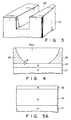
- Fig. 2A is a plan view or pattern layout showing a structure of a transistor used in a non-volatile semiconductor device according to the present invention
- Fig. 2B is a sectional view taken along A-A′ line of Fig. 2A
- Fig. 2C is a sectional view taken along B-B′ line of Fig. 2A.
- a P-well region 22 is formed on a P-type silicon substrate 21.
- a groove 23 is formed to extend in a predetermined direction as shown in Fig. 3.
- the side walls of groove 23 are formed perpendicular to the surface of P-well region 22.
- a silicon dioxide layer 24 is selectively embeded in groove 23 as shown in Fig. 4.
- groove 23 is separated into a plurality of portions 23a by silicon dioxide layer 24 and P-well region 22.
- the lower portion of silicon dioxide layer 24 embeded in groove 23 is slanted along the direction of extension of groove 23 by an angle ⁇ below 45 degrees.
- Silicon dioxide layers 25a and 25b used as first gate insulating layers are formed on side walls of groove portion 23a which are faced each other in the direction normal to the direction of extension of groove 23.
- Phosphorus-doped polysilicon layers 26a and 26b are provided on silicon dioxide layers 25a and 25b, respectively.
- a second gate insulating layer 30a (30b) which is comprised of three layers of a silicon dioxide layer 27a (27b), a silicon nitride layer 28a (28b) and a silicon dioxide layer 29a (29b).
- Phosphorus-doped polysilicon layers 31a and 31b are formed on second gate insulating layers 30a and 30b, respectively. As shown in Fig. 2A, polysilicon layers 31a and 31b are each formed to extend from groove portion 23a so that they are common to groove portion 23a and other groove portions adjacent thereto.
- N-type diffusion regions 32 each serving as the source region of a MOS transistor are formed on the surface of P-well region 22, and further an N-type diffusion region 33 serving as the drain region of the MOS transistor is formed in the surface region of P well region 22 that is located at the bottom of groove portion 23a.
- a silicon dioxide layer 34 is deposited over the entire surface of P well region 22 involving the inside of groove portion 23. An opening is formed in silicon dioxide layer 34 which reaches the surface of N-type diffusion layer 33, and a polysilicon layer 35 is formed in the opening. Polysilicon layer 35 has a low resistivity because of introduction thereto of impurities at a sufficiently high concentration. Further, a silicon dioxide layer 36 is deposited on silicon dioxide layer 34 and polysilicon layer 35. An opening is formed in silicon dioxide layer 36 which reaches the surface of polysilicon layer 35, and a metal layer 37 made of Al, Si and Cu is formed in the opening. Further, a passivation layer 38 formed of PSG, SiN or the like is deposited over metal layer 37.
- N-type diffusion layers 32 formed on the surface of P well region 22 serve as the source regions of the two non-volatile transistors
- N-type diffusion layer 33 formed at the bottom of groove portion 23a serve as the common drain region of the two non-volatile transistors.
- N-type diffusion layer 33 is connected through polysilicon layer 35 to metal layer 37 serving as the drain electrode.
- two non-volatile transistors are formed within each of groove portions 23a. And, the source region and the drain region of each transistor are separated in the direction of depth of groove portion 23a so that there is little possibility of occurrence of leak current due to scale-down of the dimensions of transistors in two dimensions. Since two transistors are formed within each of groove portions 23a, a considerable reduction in the size of transistors will be made possible. For instance, when the same design rules are applied, the size of a cell will be reduced to about 70% of the size of a cell used in a conventional memory.
- N-type diffusion regions 32 are provided on the top of the memory cell, there is no need of allowance for the formation of device-separating regions.
- polysilicon layers 26a and 26b serving as the floating gate electrodes and polysilicon layers serving as the control gate electrodes are doped with phosphorus acting as N-type impurities.
- these polysilicon layers may be doped with boron of P-type impurities.
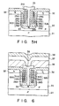
- P well region 22 is formed over the entire surface of P-type silicon substrate 21 to a thickness of about 4.5 ⁇ m.
- groove 23 of approximate depth 1.2 ⁇ m and approximate width 1.2 ⁇ m is vertically formed in P well region 22 by RIE (reactive ion etching) technique using a proper mask. It is to be noted that in Fig. 5B groove 23 is drawn larger than its actual size, and formed to extend in a predetermined direction as shown in Fig. 3.
- silicon dioxide layer 24 is deposited over the entire surface to a thickness of about 700nm (7000 ⁇ ) so that groove 23 is filled. Further, a photoresist layer 41 is deposited on silicon dioxide layer 24 to planarize the top surface of the device.
- photoresist layer 41 and silicon dioxide layer 24 are etched away to leave silicon dioxide layer 24 only within groove 23 as shown in Fig. 5D.
- a photoresist layer is formed over the entire surface of the device of Fig. 5D and then patterned to form a mask used for subsequent etching.
- Silicon dioxide layer 24 left in groove 23 is selectively etched away by isotropic etching, e.g., wet etching technique using the mask.
- silicon dioxide layer 24 is selectively left inside groove 23 so that groove 23 is separated into a plurality of groove portions 23a.
- isotropic-etching silicon dioxide layer 24 the lower end of silicon dioxide layer 24 left in groove portion 23a can be tapered at an angle ⁇ below 45 degrees as shown in Fig. 4.
- silicon dioxide layer 25 is formed over the entire surface including the inside surface of groove portion 23a at a thickness of 20nm (200 ⁇ ), and polysilicon layer 26 doped with phosphorus is deposited by CVD on silicon dioxide layer 25 to a thickness of 100nm (1000 ⁇ ).
- silicon dioxide layer 27 of a thickness of 10nm (100 ⁇ ) is formed on polysilicon layer 26 by thermal oxidation, and silicon nitride layer 28 is further deposited by CVD, at a thickness of 10nm (100 ⁇ ) over silicon dioxide layer 27.
- silicon nitride layer 28, silicon dioxide layer 27, polysilicon layer 26 and silicon dioxide layer 25 remain only on side walls of groove portion 23a in the separate form of silicon nitride layers 28a and 28b; silicon dioxide layers 27a and 27b; polysilicon layers 26a and 26b; and silicon dioxide layers 25a and 25b. They are not left on the surface of silicon dioxide layer 24 shown in Fig. 4 and at the bottom of groove portion 23a.
- anisotropic etching technique e.g., RIE technique.
- a silicon dioxide layer of a thickness of about 100nm (1000 ⁇ ) is formed only on exposed portions of polysilicon layers 26a and 26b, or the upper and lower ends thereof by heating oxidation at 900°C.
- thin silicon dioxide layers 29a and 29b have been formed on silicon nitride layers 28a and 28b.
- a Phosphorus-doped polysilicon layer of about 300nm (3000 ⁇ ) thickness is deposited over the entire surface by CVD, and the polysilicon layer is then patterned by an anisotropic etching technique, e.g., RIE technique using a mask of a predetermined shape.
- the patterning process leaves polysilicon layers 31a and 31b which are used as control electrodes of non-volatile transistors for memory cells, i.e., as a word line for memory cells.
- Silicon dioxide layer 27a, silicon nitride layer 28a and silicon dioxide layer 29a form second gate insulating layer 30a for one non-volatile transistor, while silicon dioxide layer 27b, silicon nitride layer 28b and silicon dioxide layer 29b form second gate insulating layer 30b for the other non-volatile transistor.
- a 850°C heating oxidation process is carried out to form a silicon dioxide layer 34 of 200nm (2000 ⁇ ) thickness on the surfaces of polysilicon layers 31a and 31b and N-type diffusion region 32 utilizing a difference in impurity concentrations in silicon.
- a thin silicon dioxide layer is formed at the bottom of groove portion 23a to a thickness of about 50nm (500 ⁇ ), for example.
- an anisotropic etching operation using a predetermined mask is carried out to remove only the thin silicon dioxide layer formed at the bottom of groove portion 23a, thereby exposing the surface of P well region 22.
- polysilicon layer 35 is deposited over the entire surface, and phosphorous is diffused at 1000°C from the top of polysilicon layer 35 to form N-type diffusion region 33 in the surface region of P well region 22 that is located at the bottom of groove portion 23a.
- silicon dioxide layer 36 is deposited by CVD over the entire surface to a thickness of 600nm (6000 ⁇ ), and a contact hole is then formed in silicon dioxide layer 36 to expose the surface of polysilicon layer 35.
- a layer of an alloy of Al, Si and Cu is applied over the entire surface and patterned to form metal layer 37.
- passivation layer 38 formed of PSG or SiN is deposited over the entire surface, thereby completing the device.
- groove 23 is filled with silicon dioxide layer 24 deposited by CVD and then selectively etched away.
- groove 23 may be filled with a thermal oxide layer.
- polysilicon layer 26a (26b) and polysilicon layer 31a (31b) are insulating layers of so-called ONO (Oxidi-Nitride-Oxide) structure consisting of silicon dioxide layer 27a (27b), silicon nitride layer 28a (28b) and silicon dioxide layer 29a (29b).
- ONO Oxidi-Nitride-Oxide
- a thermal oxide layer which can be formed by oxidizing the surface of the polysilicon layer 26a (26b), may be used as the second gate insulating layer.
- polysilicon layers 26a, 26b, 31a and 31b are doped with N-type phosphorous impurities. Alternatively, they may be doped with P-type boron impurities.
- control gate electrodes for non-volatile transistors are each formed of a polysilicon layer.
- two-layered control gate electrodes 53a and 53b may be used each of which is formed of a first layer 51a (51b) of polysilicon and a second layer 52a (52b) of a refractory metal silicide of molybdenum, tungsten, titanium or the like.
Landscapes
- Non-Volatile Memory (AREA)
- Semiconductor Memories (AREA)
Claims (10)
- Nichtflüchtige Speicheranordnung mit:
einem ersten Halbleiterbereich (22) eines ersten Leitfähigkeitstyps;
einem Graben (23), der in dem ersten Halbleiterbereich (22) ausgeformt ist, um sich in einer vorbestimmten Richtung zu erstrecken;
einem zweiten Halbleiterbereich (32) eines zweiten Leitfähigkeitstyps, der an der Oberfläche des ersten Halbleiterbereichs (22) ausgeformt ist, wobei er an den Graben angrenzt und als ein Source- oder Drain-Bereich dient;
wenigstens einer ersten gateisolierenden Schicht (25a, 25b), die auf einer Seitenwand eines Grabenteilgebiets (23a) ausgeformt ist, wobei die Seitenwand entlang der Richtung der Ausdehnung des Grabens (23) ist;
wenigstens einer freischwebenden Gate-Elektrode (26a, 26b), die auf einer Oberfläche der ersten gateisolierenden Schicht (25a, 25b) gegenüber deren Oberfläche ausgeformt ist, wobei sie die Seitenwand des Grabenbereichs (23a) berührt;
wenigstens einer zweiten gateisolierenden Schicht (30a, 30b), die auf einer Oberfläche der freischwebenden Gate-Elektrode (26a, 26b) gegenüber einer Oberfläche hiervon ausgeformt ist, die die erste gateisolierende Schicht (25a, 25b) berührt;
wenigstens einer Steuergateelektrode (31a, 31b, 53a, 53b), die auf einer Oberfläche der zweiten gateisolierenden Schicht (30a, 30b) gegenüber einer Oberfläche hiervon ausgeformt ist, die die freischwebende Gateelektrode (26a, 26b) berührt; und
einem dritten Halbleiterbereich (33) des zweiten Leitfähigkeitstyps, welcher in einem Oberflächenbereich des ersten Halbleiterbereichs (22) ausgeformt ist, welcher auf dem Boden des Grabenbereichs (23a) gelegen ist und welcher als ein Drain- oder Source-Bereich dient;
gekennzeichnet durch
isolierende Trennbereiche (24), welche ausgeformt sind, um die Innenseite des Grabens (23) selektiv zu füllen, um die Speicherzellenbereiche entlang der Richtung der Ausdehnung des Grabens (23) zu trennen, wobei der Grabenbereich (23a) durch isolierende Trennteilgebiete (24) und den ersten Halbleiterbereich definiert ist; und
einen vierten Halbleiterbereich (35), der im Inneren des Grabenteilgebiets (23a) ausgeformt ist, um den dritten Halbleiterbereich (33) zu berühren, und mit Dotierstoffen des zweiten Leitfähigkeitstyps dotiert ist. - Nichtflüchtige Halbleiterspeicheranordnung nach Anspruch 1, dadurch gekennzeichnet, daß die freischwebende Gate-Elektrode (26a, 26b) aus einer Polysiliziumschicht geformt ist, die mit N-Typ oder P-Typ-Dotierstoffen dotiert ist, und die Steuergateelektrode (31a, 31b) aus einer Polysiliziumschicht ausgeformt ist, die mit N-Typ oder P-Typ-Dotierstoffen dotiert ist.
- Nichtflüchtige Halbleiterspeicheranordnung nach Anspruch 1, dadurch gekennzeichnet, daß die freischwebende Gate-Elektrode (26a, 26b) aus einer Polysiliziumschicht geformt ist, die mit N-Typ oder P-Typ-Dotierstoffen dotiert ist, und die Steuergateelektrode (53a, 53b) aus einer Polysiliziumschicht (51a, 51b) und einer hochschmelzenden Metall-Siliziumschicht (52a, 52b) geformt ist.
- Nichtflüchtige Halbleiterspeicheranordnung nach Anspruch 1, dadurch gekennzeichnet, daß die isolierenden Trennbereiche (24), die im Inneren des Grabenbereichs (23a) ausgeformt sind, mit einem vorbestimmten Neigungswinkel (ϑ) entlang der Richtung der Ausdehnung des Grabens (23) ausgestattet ist.
- Nichtflüchtige Halbleiterspeicheranordnung nach Anspruch 4, dadurch gekennzeichnet, daß der Neigungswinkel (ϑ) weniger als 45° beträgt.
- Nichtflüchtige Halbleiterspeicheranordnung nach Anspruch 4, dadurch gekennzeichnet, daß die isolierenden Trennbereiche (24) jeweils aus einer Siliziumdioxidschicht geformt sind.
- Nichtflüchtige Halbleiterspeicheranordnung nach Anspruch 1, dadurch gekennzeichnet, daß die Seitenwand des Grabenteilgebiets (23a) vertikal bezüglich der Oberfläche des ersten Halbleiterbereichs (22) ausgeformt ist.
- Nichtflüchtige Halbleiterspeicheranordnung nach Anspruch 1, dadurch gekennzeichnet, daß die freischwebende Gateelektrode und die Steuergateelektrode auf jeweils gegenüberliegenden Seitenwänden des Grabens (23a) entlang der Richtung der Ausdehnung des Grabens (23) ausgeformt sind.
- Nichtflüchtige Halbleiterspeicheranordnung nach Anspruch 1, dadurch gekennzeichnet, daß der erste Halbleiterbereich (22) auf einem fünften Halbleiterbereich des ersten Leitfähigkeitstyps ausgeformt ist.
- Verfahren zur Herstellung einer nichtflüchtigen Halbleiterspeicheranordnung, welches folgende Schritte umfaßt:
Dotieren einer Oberfläche eines ersten Halbleiterbereichs (22) eines ersten Leitfähigkeitstyps mit Dotierstoffen eines zweiten Leitfähigkeitstyps, um einen zweiten Halbleiterbereich (32) auszuformen;
Ausformen eines Grabens (23) in dem ersten Halbleiterbereich (22), so daß der Halbleiterbereich an den Graben angrenzt, um sich in einer vorbestimmten Richtung durch eine anisotrope Ätztechnik auszudehnen, wobei eine vorbestimmte Maske verwendet wird;
Füllen des Grabens (23) mit einer isolierenden Drainschicht (24);
selektives Entfernen der isolierenden Drainschicht (24) durch eine anisotrope Ätztechnik, wobei eine vorbestimmte Maske verwendet wird, um den Graben (23) in eine Vielzahl von Grabenteilgebieten (23a) zu trennen;
sequentielles Formen einer ersten Siliziumdioxidschicht (25), einer ersten Polysiliziumschicht (26), einer zweiten Siliziumdioxidschicht (27) und einer Siliziumnitridschicht (28) über eine gesamte Oberfläche, wobei die Innenseitenoberflächen des Grabenteilgebiets (23a) beinhaltet sind, welches durch die isolierende Trennschicht (24) und den ersten Halbleiterbereich (22) definiert ist;
selektives Ätzen der ersten Siliziumdioxidschicht (25), der ersten Polysiliziumschicht (26), der zweiten Siliziumdioxidschicht (27) und der Siliziumnitridschicht (28), um die ersten Siliziumdioxidschichten (25a, 25b), die ersten Polysiliziumschichten (26a, 26b), die zweiten Siliziumdioxidschichten (27a, 27b) und die Siliziumnitridschichten (28a, 28b) an gegenüberliegenden Wänden des Grabenteilgebiets (23a) zurückzulassen;
Ausformen von dritten Siliziumdioxidschichten an exponierten Teilgebieten der ersten Polysiliziumschichten (26a, 26b), und von vierten Siliziumdioxidschichten (29a, 29b) auf den Oberflächen der Siliziumnitridschichten (28a, 28b) durch Heiz-Oxidationstechniken;
Ablagern einer zweiten Polysiliziumschicht auf der gesamten Oberfläche;
selektives Ätzen der zweiten Polysiliziumschicht durch eine anisotrope Ätztechnik, wobei eine vorbestimmte Maske verwendet wird, um zweite Polysiliziumschichten (31a, 31b) auf den Oberflächen der vierten Siliziumdioxidschichten (29a, 29b) zurückzulassen;
Ausformen von fünften Siliziumdioxidschichten (34) auf den zweiten Polysiliziumschichten und auf exponierten Bereichen der ersten und zweiten Halbleiterbereiche;
selektives Ätzen der fünften Siliziumdioxidschichten (34), um den ersten Halbleiterbereich (22) zu exponieren, der auf dem Boden des Grabenteilgebiets (23a) gelegen ist;
Ablagern einer dritten Polysiliziumschicht auf der gesamten Oberfläche nach der Oxidation der gesamten Oberfläche; selektives Ätzen der dritten Polysiliziumschicht durch eine anisotrope Ätztechnik, um eine dritte Polysiliziumschicht (35) wenigstens im Inneren des Grabenbereichs (23a) zurückzulassen; und
Dotieren des ersten Halbleiterbereichs (22) mit Dotierstoffen des zweiten Leitfähigkeitstyps durch die dritte Polysiliziumschicht (35), um einen dritten Halbleiterbereich (33) in einem Oberflächenbereich des ersten Halbleiterbereichs (22) auszuformen, der auf dem Boden des Grabenteilgebiets (23a) ausgeformt ist.
Applications Claiming Priority (2)
| Application Number | Priority Date | Filing Date | Title |
|---|---|---|---|
| JP62210774A JP2735193B2 (ja) | 1987-08-25 | 1987-08-25 | 不揮発性半導体装置及びその製造方法 |
| JP210774/87 | 1987-08-25 |
Publications (3)
| Publication Number | Publication Date |
|---|---|
| EP0304896A2 EP0304896A2 (de) | 1989-03-01 |
| EP0304896A3 EP0304896A3 (en) | 1990-06-13 |
| EP0304896B1 true EP0304896B1 (de) | 1993-06-23 |
Family
ID=16594920
Family Applications (1)
| Application Number | Title | Priority Date | Filing Date |
|---|---|---|---|
| EP88113799A Expired - Lifetime EP0304896B1 (de) | 1987-08-25 | 1988-08-24 | Nichtflüchtige Halbleiterspeicheranordnung und Verfahren zu ihrer Herstellung |
Country Status (5)
| Country | Link |
|---|---|
| US (1) | US4929988A (de) |
| EP (1) | EP0304896B1 (de) |
| JP (1) | JP2735193B2 (de) |
| KR (1) | KR920002091B1 (de) |
| DE (1) | DE3881986T2 (de) |
Families Citing this family (71)
| Publication number | Priority date | Publication date | Assignee | Title |
|---|---|---|---|---|
| US6081449A (en) * | 1987-05-12 | 2000-06-27 | Altera Corporation | High-density nonvolatile memory cell |
| JP2646563B2 (ja) * | 1987-07-15 | 1997-08-27 | ソニー株式会社 | 不揮発性メモリ装置 |
| JP2646591B2 (ja) * | 1987-11-27 | 1997-08-27 | ソニー株式会社 | 不揮発性メモリ装置 |
| JP2675572B2 (ja) * | 1988-03-31 | 1997-11-12 | 株式会社東芝 | 半導体集積回路の製造方法 |
| NL8900989A (nl) * | 1989-04-20 | 1990-11-16 | Philips Nv | Halfgeleiderinrichting met een in een kunststof omhulling ingebed halfgeleiderlichaam. |
| JPH02285638A (ja) * | 1989-04-27 | 1990-11-22 | Toshiba Corp | 半導体装置 |
| JPH07105453B2 (ja) * | 1989-07-13 | 1995-11-13 | 株式会社東芝 | 半導体記憶装置のセル構造 |
| US5036378A (en) * | 1989-11-01 | 1991-07-30 | At&T Bell Laboratories | Memory device |
| US4964080A (en) * | 1990-03-09 | 1990-10-16 | Intel Corporation | Three-dimensional memory cell with integral select transistor |
| US5053842A (en) * | 1990-05-30 | 1991-10-01 | Seiko Instruments Inc. | Semiconductor nonvolatile memory |
| US5078498A (en) * | 1990-06-29 | 1992-01-07 | Texas Instruments Incorporated | Two-transistor programmable memory cell with a vertical floating gate transistor |
| US5041884A (en) * | 1990-10-11 | 1991-08-20 | Mitsubishi Denki Kabushiki Kaisha | Multilayer semiconductor integrated circuit |
| US5258634A (en) * | 1991-05-17 | 1993-11-02 | United Microelectronics Corporation | Electrically erasable read only memory cell array having elongated control gate in a trench |
| JPH0567791A (ja) * | 1991-06-20 | 1993-03-19 | Mitsubishi Electric Corp | 電気的に書込および消去可能な半導体記憶装置およびその製造方法 |
| JPH0613627A (ja) * | 1991-10-08 | 1994-01-21 | Semiconductor Energy Lab Co Ltd | 半導体装置およびその作製方法 |
| US5196722A (en) * | 1992-03-12 | 1993-03-23 | International Business Machines Corporation | Shadow ram cell having a shallow trench eeprom |
| US5399516A (en) * | 1992-03-12 | 1995-03-21 | International Business Machines Corporation | Method of making shadow RAM cell having a shallow trench EEPROM |
| US5467305A (en) * | 1992-03-12 | 1995-11-14 | International Business Machines Corporation | Three-dimensional direct-write EEPROM arrays and fabrication methods |
| US5315142A (en) * | 1992-03-23 | 1994-05-24 | International Business Machines Corporation | High performance trench EEPROM cell |
| JP2889061B2 (ja) * | 1992-09-25 | 1999-05-10 | ローム株式会社 | 半導体記憶装置およびその製法 |
| US5859455A (en) * | 1992-12-31 | 1999-01-12 | Yu; Shih-Chiang | Non-volatile semiconductor memory cell with control gate and floating gate and select gate located above the channel |
| US5460988A (en) * | 1994-04-25 | 1995-10-24 | United Microelectronics Corporation | Process for high density flash EPROM cell |
| US5670803A (en) * | 1995-02-08 | 1997-09-23 | International Business Machines Corporation | Three-dimensional SRAM trench structure and fabrication method therefor |
| US6965142B2 (en) * | 1995-03-07 | 2005-11-15 | Impinj, Inc. | Floating-gate semiconductor structures |
| US5945705A (en) * | 1995-08-01 | 1999-08-31 | Advanced Micro Devices, Inc. | Three-dimensional non-volatile memory |
| US5672524A (en) * | 1995-08-01 | 1997-09-30 | Advanced Micro Devices, Inc. | Three-dimensional complementary field effect transistor process |
| JP3403877B2 (ja) * | 1995-10-25 | 2003-05-06 | 三菱電機株式会社 | 半導体記憶装置とその製造方法 |
| US5998263A (en) * | 1996-05-16 | 1999-12-07 | Altera Corporation | High-density nonvolatile memory cell |
| US6034389A (en) * | 1997-01-22 | 2000-03-07 | International Business Machines Corporation | Self-aligned diffused source vertical transistors with deep trench capacitors in a 4F-square memory cell array |
| US5929477A (en) * | 1997-01-22 | 1999-07-27 | International Business Machines Corporation | Self-aligned diffused source vertical transistors with stack capacitors in a 4F-square memory cell array |
| US5874760A (en) * | 1997-01-22 | 1999-02-23 | International Business Machines Corporation | 4F-square memory cell having vertical floating-gate transistors with self-aligned shallow trench isolation |
| US5990509A (en) * | 1997-01-22 | 1999-11-23 | International Business Machines Corporation | 2F-square memory cell for gigabit memory applications |
| US6150687A (en) | 1997-07-08 | 2000-11-21 | Micron Technology, Inc. | Memory cell having a vertical transistor with buried source/drain and dual gates |
| US6072209A (en) | 1997-07-08 | 2000-06-06 | Micro Technology, Inc. | Four F2 folded bit line DRAM cell structure having buried bit and word lines |
| US5909618A (en) | 1997-07-08 | 1999-06-01 | Micron Technology, Inc. | Method of making memory cell with vertical transistor and buried word and body lines |
| US5973356A (en) * | 1997-07-08 | 1999-10-26 | Micron Technology, Inc. | Ultra high density flash memory |
| US6717179B1 (en) | 1997-08-19 | 2004-04-06 | Semiconductor Energy Laboratory Co., Ltd. | Semiconductor device and semiconductor display device |
| US6667494B1 (en) | 1997-08-19 | 2003-12-23 | Semiconductor Energy Laboratory Co., Ltd. | Semiconductor device and semiconductor display device |
| JPH11143379A (ja) * | 1997-09-03 | 1999-05-28 | Semiconductor Energy Lab Co Ltd | 半導体表示装置補正システムおよび半導体表示装置の補正方法 |
| US6528837B2 (en) * | 1997-10-06 | 2003-03-04 | Micron Technology, Inc. | Circuit and method for an open bit line memory cell with a vertical transistor and trench plate trench capacitor |
| US5907170A (en) | 1997-10-06 | 1999-05-25 | Micron Technology, Inc. | Circuit and method for an open bit line memory cell with a vertical transistor and trench plate trench capacitor |
| US6066869A (en) * | 1997-10-06 | 2000-05-23 | Micron Technology, Inc. | Circuit and method for a folded bit line memory cell with vertical transistor and trench capacitor |
| US6025225A (en) * | 1998-01-22 | 2000-02-15 | Micron Technology, Inc. | Circuits with a trench capacitor having micro-roughened semiconductor surfaces and methods for forming the same |
| US5923063A (en) * | 1998-02-19 | 1999-07-13 | Advanced Micro Devices, Inc. | Double density V nonvolatile memory cell |
| US6246083B1 (en) | 1998-02-24 | 2001-06-12 | Micron Technology, Inc. | Vertical gain cell and array for a dynamic random access memory |
| US6124729A (en) | 1998-02-27 | 2000-09-26 | Micron Technology, Inc. | Field programmable logic arrays with vertical transistors |
| US5991225A (en) * | 1998-02-27 | 1999-11-23 | Micron Technology, Inc. | Programmable memory address decode array with vertical transistors |
| US6043527A (en) | 1998-04-14 | 2000-03-28 | Micron Technology, Inc. | Circuits and methods for a memory cell with a trench plate trench capacitor and a vertical bipolar read device |
| US6208164B1 (en) | 1998-08-04 | 2001-03-27 | Micron Technology, Inc. | Programmable logic array with vertical transistors |
| US6134175A (en) | 1998-08-04 | 2000-10-17 | Micron Technology, Inc. | Memory address decode array with vertical transistors |
| US6190968B1 (en) * | 1998-11-04 | 2001-02-20 | National Semiconductor Corporation | Method for forming EPROM and flash memory cells with source-side injection |
| US6130453A (en) * | 1999-01-04 | 2000-10-10 | International Business Machines Corporation | Flash memory structure with floating gate in vertical trench |
| US6368919B2 (en) * | 1999-01-19 | 2002-04-09 | Micron Technology, Inc. | Method and composite for decreasing charge leakage |
| TW518637B (en) | 1999-04-15 | 2003-01-21 | Semiconductor Energy Lab | Electro-optical device and electronic equipment |
| US6664909B1 (en) | 2001-08-13 | 2003-12-16 | Impinj, Inc. | Method and apparatus for trimming high-resolution digital-to-analog converter |
| US6724028B2 (en) | 2001-12-10 | 2004-04-20 | Hans Gude Gudesen | Matrix-addressable array of integrated transistor/memory structures |
| JP2003309192A (ja) * | 2002-04-17 | 2003-10-31 | Fujitsu Ltd | 不揮発性半導体メモリおよびその製造方法 |
| US6770934B1 (en) * | 2003-04-03 | 2004-08-03 | Powerchip Semiconductor Corp. | Flash memory device structure and manufacturing method thereof |
| DE10326523A1 (de) * | 2003-06-12 | 2005-01-13 | Infineon Technologies Ag | Feldeffekttransistor, insbesondere doppelt diffundierter Feldeffekttransistor, sowie Herstellungsverfahren |
| US7241654B2 (en) * | 2003-12-17 | 2007-07-10 | Micron Technology, Inc. | Vertical NROM NAND flash memory array |
| US7148538B2 (en) | 2003-12-17 | 2006-12-12 | Micron Technology, Inc. | Vertical NAND flash memory array |
| KR100526891B1 (ko) * | 2004-02-25 | 2005-11-09 | 삼성전자주식회사 | 반도체 소자에서의 버티컬 트랜지스터 구조 및 그에 따른형성방법 |
| KR100587396B1 (ko) | 2004-08-13 | 2006-06-08 | 동부일렉트로닉스 주식회사 | 비휘발성 메모리 소자 및 그의 제조방법 |
| KR100607785B1 (ko) * | 2004-12-31 | 2006-08-02 | 동부일렉트로닉스 주식회사 | 스플릿 게이트 플래시 이이피롬의 제조방법 |
| US7166888B2 (en) * | 2005-01-27 | 2007-01-23 | Micron Technology, Inc. | Scalable high density non-volatile memory cells in a contactless memory array |
| TWI274402B (en) * | 2005-06-17 | 2007-02-21 | Powerchip Semiconductor Corp | Non-volatile memory and fabricating method thereof |
| CN100385646C (zh) * | 2005-08-19 | 2008-04-30 | 力晶半导体股份有限公司 | 防止击穿的半导体元件及其制造方法 |
| CN100452355C (zh) * | 2005-08-19 | 2009-01-14 | 力晶半导体股份有限公司 | 非挥发性存储器及其制造方法 |
| US7651916B2 (en) * | 2007-01-24 | 2010-01-26 | Freescale Semiconductor, Inc | Electronic device including trenches and discontinuous storage elements and processes of forming and using the same |
| CN111508843B (zh) * | 2019-01-31 | 2023-07-14 | 中芯国际集成电路制造(上海)有限公司 | 半导体器件及其形成方法 |
| TWI896920B (zh) * | 2022-12-09 | 2025-09-11 | 華邦電子股份有限公司 | 半導體結構及其形成方法 |
Family Cites Families (6)
| Publication number | Priority date | Publication date | Assignee | Title |
|---|---|---|---|---|
| DE2706155A1 (de) * | 1977-02-14 | 1978-08-17 | Siemens Ag | In integrierter technik hergestellter elektronischer speicher |
| DE3174468D1 (en) * | 1980-09-17 | 1986-05-28 | Hitachi Ltd | Semiconductor device and method of manufacturing the same |
| US4786953A (en) * | 1984-07-16 | 1988-11-22 | Nippon Telegraph & Telephone | Vertical MOSFET and method of manufacturing the same |
| JPS61256673A (ja) * | 1985-05-08 | 1986-11-14 | Fujitsu Ltd | 半導体装置 |
| JPS6225459A (ja) * | 1985-07-25 | 1987-02-03 | Nippon Denso Co Ltd | 不揮発性半導体記憶装置 |
| US4698900A (en) * | 1986-03-27 | 1987-10-13 | Texas Instruments Incorporated | Method of making a non-volatile memory having dielectric filled trenches |
-
1987
- 1987-08-25 JP JP62210774A patent/JP2735193B2/ja not_active Expired - Fee Related
-
1988
- 1988-08-23 US US07/235,121 patent/US4929988A/en not_active Expired - Fee Related
- 1988-08-24 EP EP88113799A patent/EP0304896B1/de not_active Expired - Lifetime
- 1988-08-24 DE DE88113799T patent/DE3881986T2/de not_active Expired - Fee Related
- 1988-08-25 KR KR1019880010816A patent/KR920002091B1/ko not_active Expired
Also Published As
| Publication number | Publication date |
|---|---|
| JPS6453577A (en) | 1989-03-01 |
| KR920002091B1 (ko) | 1992-03-10 |
| EP0304896A3 (en) | 1990-06-13 |
| EP0304896A2 (de) | 1989-03-01 |
| DE3881986T2 (de) | 1993-09-30 |
| US4929988A (en) | 1990-05-29 |
| KR890004434A (ko) | 1989-04-22 |
| JP2735193B2 (ja) | 1998-04-02 |
| DE3881986D1 (de) | 1993-07-29 |
Similar Documents
| Publication | Publication Date | Title |
|---|---|---|
| EP0304896B1 (de) | Nichtflüchtige Halbleiterspeicheranordnung und Verfahren zu ihrer Herstellung | |
| US6803279B2 (en) | NROM fabrication method | |
| KR100429954B1 (ko) | 불휘발성 반도체 기억 장치를 포함하는 반도체 집적 회로장치의 제조 방법 | |
| US5070032A (en) | Method of making dense flash eeprom semiconductor memory structures | |
| US7091087B2 (en) | Optimized flash memory cell | |
| US5966603A (en) | NROM fabrication method with a periphery portion | |
| US5270240A (en) | Four poly EPROM process and structure comprising a conductive source line structure and self-aligned polycrystalline silicon digit lines | |
| KR100429958B1 (ko) | 불휘발성 반도체 기억 장치를 포함하는 반도체 집적 회로장치 | |
| US6699753B2 (en) | Method of fabricating an array of non-volatile memory cells | |
| EP0503205B1 (de) | EPROM und Verfahren zur Herstellung | |
| US5389808A (en) | Non-volatile semiconductor memory with increased capacitance between floating and control gates | |
| US5268585A (en) | Non-volatile memory and method of manufacturing the same | |
| US20030058705A1 (en) | Semiconductor device and method of manufacturing the same | |
| JPH0560671B2 (de) | ||
| US6743674B2 (en) | Method of forming a semiconductor array of floating gate memory cells and strap regions, and a memory array and strap regions made thereby | |
| US6773974B2 (en) | Method of forming a semiconductor array of floating gate memory cells and strap regions | |
| JPH0817948A (ja) | 半導体装置及びその製造方法 | |
| GB2080024A (en) | Semiconductor Device and Method for Fabricating the Same | |
| JPH08162547A (ja) | 半導体記憶装置 | |
| JP3431860B2 (ja) | 側壁フローティング・ゲートを有するフラッシュ・メモリの製造方法 | |
| US20040217411A1 (en) | Non-volatile semiconductor memory device and manufacturing method therefor | |
| US7276761B2 (en) | Semiconductor memory device having insulating film of varying thickness over bit lines | |
| US6274433B1 (en) | Methods and arrangements for forming a floating gate in non-volatile memory semiconductor devices | |
| JPH05167033A (ja) | 半導体装置、半導体記憶装置およびその製造方法 | |
| JP2846306B2 (ja) | 半導体記憶装置およびその製造方法 |
Legal Events
| Date | Code | Title | Description |
|---|---|---|---|
| PUAI | Public reference made under article 153(3) epc to a published international application that has entered the european phase |
Free format text: ORIGINAL CODE: 0009012 |
|
| 17P | Request for examination filed |
Effective date: 19880921 |
|
| AK | Designated contracting states |
Kind code of ref document: A2 Designated state(s): DE FR GB |
|
| PUAL | Search report despatched |
Free format text: ORIGINAL CODE: 0009013 |
|
| AK | Designated contracting states |
Kind code of ref document: A3 Designated state(s): DE FR GB |
|
| 17Q | First examination report despatched |
Effective date: 19920316 |
|
| GRAA | (expected) grant |
Free format text: ORIGINAL CODE: 0009210 |
|
| AK | Designated contracting states |
Kind code of ref document: B1 Designated state(s): DE FR GB |
|
| REF | Corresponds to: |
Ref document number: 3881986 Country of ref document: DE Date of ref document: 19930729 |
|
| ET | Fr: translation filed | ||
| PLBE | No opposition filed within time limit |
Free format text: ORIGINAL CODE: 0009261 |
|
| STAA | Information on the status of an ep patent application or granted ep patent |
Free format text: STATUS: NO OPPOSITION FILED WITHIN TIME LIMIT |
|
| 26N | No opposition filed | ||
| PGFP | Annual fee paid to national office [announced via postgrant information from national office to epo] |
Ref country code: FR Payment date: 19970811 Year of fee payment: 10 |
|
| PGFP | Annual fee paid to national office [announced via postgrant information from national office to epo] |
Ref country code: DE Payment date: 19970901 Year of fee payment: 10 |
|
| REG | Reference to a national code |
Ref country code: GB Ref legal event code: 746 Effective date: 19981026 |
|
| PG25 | Lapsed in a contracting state [announced via postgrant information from national office to epo] |
Ref country code: FR Free format text: LAPSE BECAUSE OF NON-PAYMENT OF DUE FEES Effective date: 19990430 |
|
| PG25 | Lapsed in a contracting state [announced via postgrant information from national office to epo] |
Ref country code: DE Free format text: LAPSE BECAUSE OF NON-PAYMENT OF DUE FEES Effective date: 19990601 |
|
| REG | Reference to a national code |
Ref country code: FR Ref legal event code: ST |
|
| REG | Reference to a national code |
Ref country code: GB Ref legal event code: IF02 |
|
| PGFP | Annual fee paid to national office [announced via postgrant information from national office to epo] |
Ref country code: GB Payment date: 20070822 Year of fee payment: 20 |
|
| REG | Reference to a national code |
Ref country code: GB Ref legal event code: PE20 Expiry date: 20080823 |
|
| PG25 | Lapsed in a contracting state [announced via postgrant information from national office to epo] |
Ref country code: GB Free format text: LAPSE BECAUSE OF EXPIRATION OF PROTECTION Effective date: 20080823 |