EP0307844A2 - Circuit intégré semi-conducteur comprenant une configuration d'interconnexion à flexibilité améliorée - Google Patents
Circuit intégré semi-conducteur comprenant une configuration d'interconnexion à flexibilité améliorée Download PDFInfo
- Publication number
- EP0307844A2 EP0307844A2 EP88114886A EP88114886A EP0307844A2 EP 0307844 A2 EP0307844 A2 EP 0307844A2 EP 88114886 A EP88114886 A EP 88114886A EP 88114886 A EP88114886 A EP 88114886A EP 0307844 A2 EP0307844 A2 EP 0307844A2
- Authority
- EP
- European Patent Office
- Prior art keywords
- layer
- type
- substrate
- integrated circuit
- semiconductor
- Prior art date
- Legal status (The legal status is an assumption and is not a legal conclusion. Google has not performed a legal analysis and makes no representation as to the accuracy of the status listed.)
- Withdrawn
Links
Images


Classifications
-
- H—ELECTRICITY
- H10—SEMICONDUCTOR DEVICES; ELECTRIC SOLID-STATE DEVICES NOT OTHERWISE PROVIDED FOR
- H10W—GENERIC PACKAGES, INTERCONNECTIONS, CONNECTORS OR OTHER CONSTRUCTIONAL DETAILS OF DEVICES COVERED BY CLASS H10
- H10W20/00—Interconnections in chips, wafers or substrates
- H10W20/20—Interconnections within wafers or substrates, e.g. through-silicon vias [TSV]
-
- H—ELECTRICITY
- H10—SEMICONDUCTOR DEVICES; ELECTRIC SOLID-STATE DEVICES NOT OTHERWISE PROVIDED FOR
- H10W—GENERIC PACKAGES, INTERCONNECTIONS, CONNECTORS OR OTHER CONSTRUCTIONAL DETAILS OF DEVICES COVERED BY CLASS H10
- H10W20/00—Interconnections in chips, wafers or substrates
- H10W20/40—Interconnections external to wafers or substrates, e.g. back-end-of-line [BEOL] metallisations or vias connecting to gate electrodes
- H10W20/41—Interconnections external to wafers or substrates, e.g. back-end-of-line [BEOL] metallisations or vias connecting to gate electrodes characterised by their conductive parts
- H10W20/427—Power or ground buses
-
- H—ELECTRICITY
- H10—SEMICONDUCTOR DEVICES; ELECTRIC SOLID-STATE DEVICES NOT OTHERWISE PROVIDED FOR
- H10W—GENERIC PACKAGES, INTERCONNECTIONS, CONNECTORS OR OTHER CONSTRUCTIONAL DETAILS OF DEVICES COVERED BY CLASS H10
- H10W70/00—Package substrates; Interposers; Redistribution layers [RDL]
- H10W70/40—Leadframes
- H10W70/464—Additional interconnections in combination with leadframes
- H10W70/465—Bumps or wires
-
- H—ELECTRICITY
- H10—SEMICONDUCTOR DEVICES; ELECTRIC SOLID-STATE DEVICES NOT OTHERWISE PROVIDED FOR
- H10W—GENERIC PACKAGES, INTERCONNECTIONS, CONNECTORS OR OTHER CONSTRUCTIONAL DETAILS OF DEVICES COVERED BY CLASS H10
- H10W72/00—Interconnections or connectors in packages
- H10W72/01—Manufacture or treatment
- H10W72/015—Manufacture or treatment of bond wires
-
- H—ELECTRICITY
- H10—SEMICONDUCTOR DEVICES; ELECTRIC SOLID-STATE DEVICES NOT OTHERWISE PROVIDED FOR
- H10W—GENERIC PACKAGES, INTERCONNECTIONS, CONNECTORS OR OTHER CONSTRUCTIONAL DETAILS OF DEVICES COVERED BY CLASS H10
- H10W72/00—Interconnections or connectors in packages
- H10W72/50—Bond wires
-
- H—ELECTRICITY
- H10—SEMICONDUCTOR DEVICES; ELECTRIC SOLID-STATE DEVICES NOT OTHERWISE PROVIDED FOR
- H10W—GENERIC PACKAGES, INTERCONNECTIONS, CONNECTORS OR OTHER CONSTRUCTIONAL DETAILS OF DEVICES COVERED BY CLASS H10
- H10W72/00—Interconnections or connectors in packages
- H10W72/90—Bond pads, in general
- H10W72/931—Shapes of bond pads
- H10W72/932—Plan-view shape, i.e. in top view
Definitions
- the present invention generally relates to semiconductor integrated circuits, and more particularly to a bipolar semiconductor integrated circuit.
- the integration density of semiconductor integrated circuits is rapidly improving due to the progress in lithography techniques and the like.
- the number of signal interconnections within the integrated circuit is increasing, and a region for providing power source interconnections for supplying power source voltages is increasing because of the increase in the power consumption of the integrated circuit.
- the number of multi-level interconnections is limited to approximately three because deficiencies such as a disconnection and inconsistent thickness of the interconnection are easily generated when four or more levels of interconnections are stacked. Consequently, the chip size becomes large because of the need to increase the signal interconnections in each level and to widen the power source interconnections. Hence, there is a demand to prevent such an increase of the chip size.
- the length of the signal interconnection is long, it is impossible to realize a high-speed circuit operation even when high-speed circuit elements are used.
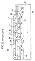
- FIGS.1A and 1B are a plan view and a cross sectional view respectively showing an example of a conventional semiconductor integrated circuit.
- a semiconductor chip 12 is accommodated within a stage 11 of a package 10.
- Terminals 13 for signal input and output and terminals 14 for supplying power source voltages V CC and V EE are provided on the semiconductor chip 12, and these terminals 13 and 14 are wire-bonded on package leads 15.
- a first power source interconnection (not shown) for the power source voltage V CC and a second power source interconnection 16 for the power source voltage V EE are provided on the semiconductor chip 12.
- the first and second power source interconnections respectively have stripe patterns which intersect each other in the plan view.
- an emitter coupled logic (ECL) circuit is formed between the first and second power source interconnections.
- FIG.2 shows a cross sectional view of the semiconductor chip 12.
- the semiconductor chip 12 has a p ⁇ -type substrate 21 provided with a metallized layer 20 on a back surface thereof.
- An n+-type buried layer 22, an n-type epitaxial layer 23, a p+-type isolation layer 24, a p-type diffusion layer 25 which becomes a base, an n+-type diffusion layer 26 which becomes an emitter, an n+-type diffusion layer 27 which becomes a collector, and a p-type diffusion layer 28 which becomes a resistor are provided on a front surface of the p ⁇ -type substrate 21.
- the semiconductor chip 12 has insulator layers 29 and 30 indicated by hatchings, a first interconnection 31, and a second interconnection 32.
- the second interconnection 32 corresponds to the second power source interconnection 16 for the power source voltage V EE shown in FIGS.1A and 1B.
- the power source interconnection is an aluminum interconnection having a current density of 2 x 10⁵ A/cm2 and a thickness of 1 micron
- the power source interconnection needs a large width of 0.5 mm.
- the substrate 21 Because of the need to reduce the capacitance between the collector and the substrate, that is, mainly the capacitance introduced between the n+-type buried layer 22 and the substrate 21, the substrate 21 has a low impurity density with a high resistivity in the range of 5 ⁇ cm to 30 ⁇ cm. Normally, the substrate 21 has a thickness of 500 microns, and for this reason, it is impossible to supply the power source voltage from the back surface of the substrate 21 when the voltage drop is taken into account. Thus, the first and second interconnections 31 and 32 are used to supply the power source voltages.
- the conventional semiconductor integrated circuit suffers problems in that the voltage drop is large due to the long power source interconnections, and the freedom with which the signal interconnections may be designed is limited because the signal interconnections must be positioned avoiding the power source interconnections. In other words, the design flexibility of the interconnection is poor in the conventional integrated circuit. Furthermore, there is another problem in that the chip size becomes large because of the need to provide a large number of terminals for the power source voltages on the semiconductor chip.
- Another and more specific object of the present invention is to provide a semiconductor integrated circuit in which a power source voltage is supplied to a circuit element forming layer from a conductive layer through a substrate and a certain region made of a semiconductor type identical to that of the substrate or through the substrate and a certain region made of a metal material.
- the conductive layer is formed on one side of the substrate, and the certain region makes contact with the other side of the substrate.
- the circuit element forming layer is provided on the other side of the substrate and connects to the certain region.
- Still another object of the present invention is to provide a semiconductor integrated circuit comprising a substrate of a first semiconductor type having a first impurity density, where the first semiconductor type is one of p-type and n-type semiconductors, a conductive layer formed on a back surface of the substrate, a first layer of the first semiconductor type formed on a front surface of the substrate and having a second impurity density lower than the first impurity density, a second layer of a second semiconductor type formed on the first layer for forming circuit elements therein, where the second semiconductor type is the other of the p-type and n-type semiconductors, and a region of the first semiconductor type extending from a top surface of the second layer and reaching at least the first layer.
- the conductive layer, the first layer and the region form a conductive path for supplying a power source voltage to the circuit elements in the second layer from the back surface of the substrate.
- the length of the power source interconnection is shortened and the voltage drop can be decreased compared to the conventional semiconductor integrated circuit.
- the noise margin is improved and it is possible to realize a high-speed circuit operation.
- the conductor path for supplying the power source voltage is arranged vertically on the substrate, the signal interconnections can be designed with a large degree of freedom thereby making it possible to prevent the chip size from increasing.
- FIG.3 is a cross sectional view showing a semiconductor chip of a first embodiment of a semiconductor integrated circuit according to the present invention.
- a p+-type substrate 41 of a semiconductor chip 50 has a high impurity density with a resistivity of 0.1 ⁇ cm or less.
- a metallized layer (conductive layer) 42 is provided on a back surface of the p+-type substrate 41.
- a p ⁇ -type epitaxial layer (first p-type layer) 43 having a high resistivity in the range of 1 ⁇ cm to 30 ⁇ cm is formed on a front surface of the p+-type substrate 41.
- a p+-type layer (second p-type layer) or region 44 having a low resistivity is selectively formed within the p ⁇ -type epitaxial layer 43.
- an n+-type buried layer 22a, an n-type epitaxial layer 23a, a p+-type isolation layer or region 24a, a p-type diffusion layer 25a which becomes a base, an n+-type diffusion layer 26a which becomes an emitter, an n+-type diffusion layer 27a which becomes a collector, and a p-type diffusion layer 28a which becomes a resistor are provided on the front surface of the p+-type substrate 41.
- the semiconductor chip 50 has insulator layers 29a and 30a indicated by hatchings, a first interconnection 31a, and a second interconnection 32a.
- a conductor path is formed from the metallized layer 42 to the first and second interconnections 31a and 32a through the p+-type substrate 41 having the low resistivity, the p+-type layer 44 and the p+-type isolation layer 24a.
- the second interconnection 32a is connected to transistors and resistor elements formed on the substrate surface.
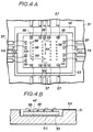
- FIGS.4A and 4B are a plan view and a cross sectional view respectively showing the first embodiment of a semiconductor integrated circuit according to the present invention.
- a metallized layer 53 is provided on approximately the entire surface of the stage 52 of the package 51.
- the metallized layer 53 is connected to package leads 54 for the power source voltage V EE .
- the semiconductor chip 50 is connected to the package 51 with the metallized layer 42 of the semiconductor chip 50 in contact with the metallized layer 53 of the package 51.
- Terminals 55 for signal input and output and terminals 56 for supplying the power source voltage V CC are provided on the semiconductor chip 50, and these terminals 55 and 56 are connected to package leads 57 by wire-bonding or the like.
- the power source voltage V EE is supplied to the semiconductor chip 50 through the package lead 54 and the metallized layer 53, and the power source voltage V EE is passed through the p+-type substrate 41, the p+-type layer 44 and the p+-type isolation layer 24a. Finally, the power source voltage V EE obtained through these layers is supplied to the ECL circuit or the like within the semiconductor chip 50 through the first and second interconnections 31a and 32a. Interconnections 58 for supplying the power source voltage V EE on the semiconductor chip 50 are shown in FIG.4A.
- the interconnections 58 each occupy a small area and are scattered in the plan view in FIG.4A.
- the signal interconnections may be provided between the interconnections 58 as indicated by arrows 59, and the signal interconnections may be designed with a large degree of freedom.
- the power source voltage V EE is supplied from the back surface of the semiconductor chip 50 at a position of the circuit which requires the power source voltage V EE in the plan view. In other words, the power source voltage V EE is supplied to the circuit in a vertical path in the cross sectional view. For this reason, it is possible to make the interconnection for supplying the power source voltage V EE extremely short.
- the resistivity of the conductive path in the semiconductor chip 50 from the metallized layer 42 to the first and second interconnections 31a and 32a through the p+-type substrate 41, the p+-type layer 44 and the p+-type isolation layer 24a can be appropriately selected by changing the cross sectional area and/or the density of the p-type impurity of the conductive path and/or the thickness of the p-type layer 43.
- the voltage drop due to a current of 1 mA is 5 mV.
- the p+-type substrate 41 has a size of 5 mm by 5 mm and a thickness t of 0.5 mm and a resistivity of 0.01 ⁇ cm
- this voltage drop V is approximately 2 mV. Therefore, a total voltage drop is approximately 7 mV which is considerably small compared to the conventional case where the total voltage drop would be 50 mV or more.
- connection of the semiconductor chip 50 to the package 51 is made by die-bonding the semiconductor chip 50 on the stage 52.
- the power source voltage V EE can be stably supplied to the semiconductor chip 50 without wire-bonding.
- the problem of electromigration will not occur because the length of the metal interconnection (first and second interconnections 31a and 32a) for the power source voltage V EE can be made short and the current density can be made small.
- the p+-type substrate 41 Since the p+-type substrate 41 has the high impurity density, it is possible to prevent the p-type substrate from being transformed into an n-type due to oxygen and carbon which are included in the silicon substrate produced by the Czochralski method and act as impurity donors. In addition, because the p-type layer 43 having the low impurity density makes contact with the n-type epitaxial layer 23a, a pn junction capacitance thereof can be made small.
- FIG.5 is a circuit diagram showing an ECL circuit within the semiconductor chip 50.
- transistors Trl, Tr2 and Tr3 and resistors Rl, R2 and R3 are connected as shown.
- V EE denotes a power source voltage
- V BB and V CS denote reference voltages
- GND denotes the ground voltage
- IN denotes an input of the ECL circuit
- OUT denotes an output of the ECL circuit.
- FIG.6 shows on an enlarged scale a plan view of the interconnections for realizing the ECL circuit shown in FIG.5 on the first embodiment of the semiconductor integrated circuit.
- those parts which are the same as those corresponding parts in FIGS.3, 4A, 4B and 5 are designated by the same reference numerals, and a description thereof will be omitted.
- the interconnections are shown with hatchings.
- B, E and C respectively denote the base, emitter and collector of the transistors Trl through Tr3. It is of course possible to connect a terminal of the resistor R3 to be coupled to the power source voltage V EE directly to the p+-type isolation layer 24a instead of through a metal interconnection (58).
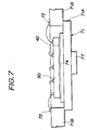
- FIG.7 is a cross sectional view showing a modification of the first embodiment of the semiconductor integrated circuit according to the present invention.
- a package 71 has a copper (Cu) portion 71A and a ceramic portion 71B.
- a molybdenum (Mo) interconnection 74 is provided on the Cu portion 71A.
- Package leads 72 are formed on the ceramic portion 71B, and terminals for signal input and output and terminals for supplying the power source voltage V CC respectively provided on the semiconductor chip 50 are connected to the package leads 72 by a wire-bonding or other methods.
- the semiconductor chip 50 is mounted on the package 71 so that the metallized layer 42 makes contact with the Mo interconnection 74.
- An electrode 77 is provided on the Cu portion 71A, and the power source voltage V EE is supplied from the electrode 77.
- FIG.8 a cross sectional view of a semiconductor chip of the second embodiment shown in FIG.8.
- FIG.8 those parts which are essentially the same as those corresponding parts in FIG.3 are designated by the same reference numerals, and a description thereof will be omitted.
- the p+-type isolation layer 24a is used in common as an isolation layer for isolating a circuit element forming layer (23a) along the horizontal direction and as a portion of the conductive path for supplying the power source voltage V EE .
- a trench isolation 81 is used to isolate the circuit element forming layer of a semiconductor chip 80 along the horizontal direction, and the conductive path is formed independently of the trench isolation 81.
- a p+-type layer or region 44a is formed to extend from the n-type epitaxial layer 23a to the p+-type substrate 41.
- the power source voltage V EE is supplied to the semiconductor chip 80 through the p+-type substrate 41 and the p+-type layer 44a. Finally, the power source voltage V EE obtained through these layers is supplied to the ECL circuit or the like within the semiconductor chip 80 through the first and second interconnections (not shown in FIG.8).
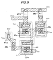
- FIG.9 shows on an enlarged scale a plan view of the interconnections for realizing the ECL circuit shown in FIG.5 on the second embodiment of the semiconductor integrated circuit.
- FIG.6 those parts which are the same as those corresponding parts in FIGS.5 and 8 are designated by the same reference numerals, and a description thereof will be omitted.
- the interconnections are shown with hatchings.
- the power source voltage V EE is supplied from the back surface of the substrate. For this reason, there is no need to provide terminals for supplying the power source voltage V EE on top of the semiconductor chip and it is possible to provide that much more terminals (or pads) for signals on top of the semiconductor chip without increasing the chip size.
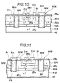
- FIG.10 shows a third embodiment of the semiconductor integrated circuit according to the present invention
- FIG.11 shows a modification of the third embodiment.
- FIGS.10 and 11 those parts which are essentially the same as those corresponding parts in FIG.8 are designated by the same reference numerals, and a description thereof will be omitted.
- the third embodiment and the modification thereof employ a trench connecting means 90A similar to the trench isolation 81, as a means for connecting the circuit element forming layer to a p+-type substrate 41A or a n+-type substrate 41B.
- a silicon oxide layer 91 is formed on only side surfaces of U-grooves 89 which extend into the p+-type substrate 41A, and the inside of the U-grooves 89 is filled by a conductive filler material 92A such as a p-type polysilicon and a metal such as tungsten (W).
- the U-grooves 89 have an approximate U-shape.
- a trench connecting means 90B similar to that of the third embodiment is formed on the n+-type substrate 41B.
- a conductive filler material 92B is an n-type polysilicon or a metal such as W.
- a most negative power source voltage (for example, V EE or the like) is connected to the substrate 41A because the p-type polysilicon or the metal fills the U-grooves 89 of the trench connecting means 90A.
- a most positive power source voltage is supplied to the circuit element forming layer through the power source interconnection (for example, Al interconnection and not shown) provided on the top side of the semiconductor integrated circuit.
- a most positive power source voltage (for example, GND) is connected to the substrate 41B because the n-type polysilicon or the metal fills the U-grooves 89 of the trench connecting means 90B.
- a most negative power source voltage is supplied to the circuit element forming layer through the power source interconnection (not shown) provided on the top side of the semiconductor integrated circuit.
- FIG.12 shows a fourth embodiment of the semiconductor integrated circuit according to the present invention.
- those parts which are essentially the same as those corresponding parts in FIGS.10 and 11 are designated by the same reference numerals, and a description thereof will be omitted.
- an insulator layer 43a made of SiO2 or the like is formed between a substrate 41C and the n+-type buried layer 22a which is connected to the n+-type diffusion layer 27a which becomes the collector so as to further reduce the parasitic capacitance between the substrate 41C and the n+-type buried layer 22a.
- the insulator layer 43a is interposed between the low resistivity substrate 41C which may be a p-type or an n-type substrate and the circuit element forming layer including the n+-type buried layer 22a and the n-type epitaxial layer 23a, and trench connecting means 90C are formed similarly as in the third embodiment (and modification thereof) as shown in FIG.12.
- the silicon oxide layer 91 is formed on only side surfaces of the U-grooves 89 which penetrate the insulator layer 43a and extend into the substrate 41C, and the inside of the U-grooves 89 is filled by a conductive filler material 92C such as a p-type or an n-type polysilicon and a metal such as tungsten (W).
- the p-type or n-type polysilicon is used as the conductive filler material 92C depending on whether the substrate 41C is p-type or n-type.
- An insulator layer 29b is formed on the second interconnection 32a, and a third interconnection 99 is formed on the insulator layer 29b. According to this embodiment, it is possible to minimize the parasitic capacitance between the substrate 41 and the collector region.
- the power source voltages V EE and V CC are used because the description is given of the case where ECL circuits are formed in the semiconductor chip.
- the power source voltage V CC is the ground voltage GND and the power source voltage V EE is -5.2 V, for example.
- TTL transistor transistor logic
- a p-type substrate is used in the described embodiments, but it is of course possible to use an n-type substrate. In this case, however, a highest power source voltage is supplied from the back surface of the substrate.
Landscapes
- Semiconductor Integrated Circuits (AREA)
- Internal Circuitry In Semiconductor Integrated Circuit Devices (AREA)
- Design And Manufacture Of Integrated Circuits (AREA)
- Bipolar Transistors (AREA)
- Bipolar Integrated Circuits (AREA)
Applications Claiming Priority (2)
| Application Number | Priority Date | Filing Date | Title |
|---|---|---|---|
| JP62230258A JPS6473669A (en) | 1987-09-14 | 1987-09-14 | Semiconductor integrated circuit |
| JP230258/87 | 1987-09-14 |
Publications (2)
| Publication Number | Publication Date |
|---|---|
| EP0307844A2 true EP0307844A2 (fr) | 1989-03-22 |
| EP0307844A3 EP0307844A3 (fr) | 1989-07-19 |
Family
ID=16904984
Family Applications (1)
| Application Number | Title | Priority Date | Filing Date |
|---|---|---|---|
| EP88114886A Withdrawn EP0307844A3 (fr) | 1987-09-14 | 1988-09-12 | Circuit intégré semi-conducteur comprenant une configuration d'interconnexion à flexibilité améliorée |
Country Status (4)
| Country | Link |
|---|---|
| US (1) | US5072274A (fr) |
| EP (1) | EP0307844A3 (fr) |
| JP (1) | JPS6473669A (fr) |
| KR (1) | KR910009422B1 (fr) |
Cited By (4)
| Publication number | Priority date | Publication date | Assignee | Title |
|---|---|---|---|---|
| DE3931381A1 (de) * | 1989-09-20 | 1991-03-28 | Siemens Ag | Halbleiterschichtaufbau mit vergrabener verdrahtungsebene, verfahren fuer dessen herstellung und anwendung der vergrabenen verdrahtungsebene als vergrabene zellplatte fuer drams |
| EP0495974A4 (en) * | 1990-08-06 | 1993-06-23 | Harris Corporation | Trench conductors and crossover architecture |
| US5283461A (en) * | 1990-08-06 | 1994-02-01 | Harris Corporation | Trench conductor and crossunder architecture |
| EP0513764A3 (en) * | 1991-05-13 | 1994-06-22 | Toshiba Kk | Semiconductor device and method of increasing device breakdown voltage of semiconductor device |
Families Citing this family (9)
| Publication number | Priority date | Publication date | Assignee | Title |
|---|---|---|---|---|
| US5482897A (en) * | 1994-07-19 | 1996-01-09 | Lsi Logic Corporation | Integrated circuit with on-chip ground plane |
| US6232649B1 (en) * | 1994-12-12 | 2001-05-15 | Hyundai Electronics America | Bipolar silicon-on-insulator structure and process |
| JP3602242B2 (ja) * | 1996-02-14 | 2004-12-15 | 株式会社ルネサステクノロジ | 半導体装置 |
| JPH10247713A (ja) * | 1997-03-05 | 1998-09-14 | Toshiba Corp | 半導体素子、半導体装置及びこれらの製造方法 |
| JP4626935B2 (ja) * | 2002-10-01 | 2011-02-09 | ルネサスエレクトロニクス株式会社 | 半導体装置及びその製造方法 |
| US6993447B2 (en) * | 2003-08-26 | 2006-01-31 | Oki Electric Industry Co., Ltd. | System LSI |
| DE102004028679A1 (de) * | 2004-06-14 | 2006-01-05 | Infineon Technologies Ag | Isolationsgrabenanordnung |
| JP2006196802A (ja) * | 2005-01-17 | 2006-07-27 | Sony Corp | 半導体装置および半導体装置の製造方法 |
| DE102006013203B3 (de) * | 2006-03-22 | 2008-01-10 | Infineon Technologies Ag | Integrierte Halbleiteranordnung mit Rückstromkomplex zur Verringerung eines Substratstroms und Verfahren zu deren Herstellung |
Family Cites Families (12)
| Publication number | Priority date | Publication date | Assignee | Title |
|---|---|---|---|---|
| US3581165A (en) * | 1967-01-23 | 1971-05-25 | Motorola Inc | Voltage distribution system for integrated circuits utilizing low resistivity semiconductive paths for the transmission of voltages |
| DE1639176B2 (de) * | 1968-02-23 | 1971-02-25 | Integrierte festkoerperschaltung mit lediglich zwei elektrodenzuleitungen | |
| FR2373163A1 (fr) * | 1976-12-03 | 1978-06-30 | Thomson Csf | Structure pour circuits logiques |
| FR2374743A1 (fr) * | 1976-12-20 | 1978-07-13 | Radiotechnique Compelec | Transistor multicouche a emetteur compose |
| US4266238A (en) * | 1977-03-11 | 1981-05-05 | Zaidan Hojin Handotai Kenkyu Shinkokai | Semiconductor device having high-speed operation and integrated circuit using same |
| FR2464562A1 (fr) * | 1979-08-28 | 1981-03-06 | Thomson Csf | Transistor a effet de champ comprenant des chemins conducteurs realises sous forme de rainures recouvertes de metal et atteignant un substrat tres dope |
| US4511220A (en) * | 1982-12-23 | 1985-04-16 | The United States Of America As Represented By The Secretary Of The Air Force | Laser target speckle eliminator |
| JPS59124153A (ja) * | 1982-12-29 | 1984-07-18 | Matsushita Electric Ind Co Ltd | 半導体集積回路装置 |
| US4661202A (en) * | 1984-02-14 | 1987-04-28 | Kabushiki Kaisha Toshiba | Method of manufacturing semiconductor device |
| EP0256315B1 (fr) * | 1986-08-13 | 1992-01-29 | Siemens Aktiengesellschaft | Circuit intégré contenant des transistors bipolaires et de type CMOS sur le même substrat et son procédé de fabrication |
| US4819052A (en) * | 1986-12-22 | 1989-04-04 | Texas Instruments Incorporated | Merged bipolar/CMOS technology using electrically active trench |
| JPS63198367A (ja) * | 1987-02-13 | 1988-08-17 | Toshiba Corp | 半導体装置 |
-
1987
- 1987-09-14 JP JP62230258A patent/JPS6473669A/ja active Pending
-
1988
- 1988-09-12 EP EP88114886A patent/EP0307844A3/fr not_active Withdrawn
- 1988-09-14 KR KR1019880011860A patent/KR910009422B1/ko not_active Expired
-
1990
- 1990-12-10 US US07/624,467 patent/US5072274A/en not_active Expired - Fee Related
Cited By (5)
| Publication number | Priority date | Publication date | Assignee | Title |
|---|---|---|---|---|
| DE3931381A1 (de) * | 1989-09-20 | 1991-03-28 | Siemens Ag | Halbleiterschichtaufbau mit vergrabener verdrahtungsebene, verfahren fuer dessen herstellung und anwendung der vergrabenen verdrahtungsebene als vergrabene zellplatte fuer drams |
| EP0495974A4 (en) * | 1990-08-06 | 1993-06-23 | Harris Corporation | Trench conductors and crossover architecture |
| US5283461A (en) * | 1990-08-06 | 1994-02-01 | Harris Corporation | Trench conductor and crossunder architecture |
| EP0513764A3 (en) * | 1991-05-13 | 1994-06-22 | Toshiba Kk | Semiconductor device and method of increasing device breakdown voltage of semiconductor device |
| US5554872A (en) * | 1991-05-13 | 1996-09-10 | Kabushiki Kaisha Toshiba | Semiconductor device and method of increasing device breakdown voltage of semiconductor device |
Also Published As
| Publication number | Publication date |
|---|---|
| JPS6473669A (en) | 1989-03-17 |
| US5072274A (en) | 1991-12-10 |
| EP0307844A3 (fr) | 1989-07-19 |
| KR910009422B1 (ko) | 1991-11-15 |
| KR890005875A (ko) | 1989-05-17 |
Similar Documents
| Publication | Publication Date | Title |
|---|---|---|
| US5072274A (en) | Semiconductor integrated circuit having interconnection with improved design flexibility | |
| US3808475A (en) | Lsi chip construction and method | |
| IE53844B1 (en) | Semiconductor integrated circuit comprising a semiconductor substrate and interconnecting layers | |
| US6662344B2 (en) | Semiconductor device and method for fabricating the same | |
| US4480319A (en) | Emitter coupled flip flop memory with complementary bipolar loads | |
| US4701777A (en) | Gate array type semiconductor integrated circuit device | |
| US5631181A (en) | Method of making a monolithic diode array | |
| US5060046A (en) | Semiconductor integrated circuit device having enlarged cells formed on ends of basic cell arrays | |
| US5065216A (en) | Semiconductor integrated circuit having interconnection with improved design flexibility, and method of production | |
| US5444288A (en) | CMOS integrated circuit having improved power-supply filtering | |
| US4417265A (en) | Lateral PNP power transistor | |
| US3913123A (en) | Bipolar type semiconductor integrated circuit | |
| US4952997A (en) | Semiconductor integrated-circuit apparatus with internal and external bonding pads | |
| US4631570A (en) | Integrated circuit having buried oxide isolation and low resistivity substrate for power supply interconnection | |
| EP0011961B1 (fr) | Circuit de sortie à trois états | |
| US5240867A (en) | Semiconductor integrated circuit having interconnection with improved design flexibility, and method of production | |
| US5023482A (en) | ISL to TTL translator | |
| CA1134054A (fr) | Circuit integre | |
| US4595942A (en) | Integrated circuit | |
| JPS58165A (ja) | 集積回路パワ−トランジスタアレイ | |
| US4388636A (en) | Static memory cell and memory constructed from such cells | |
| EP0074804A2 (fr) | Circuit intégré à semi-conducteur comprenant un substrat semi-conducteur et des couches d'interconnexion | |
| EP0056191A2 (fr) | Logique d'injection intégrée | |
| CA1129973A (fr) | Circuit logique integre | |
| KR910002036B1 (ko) | 반도체 집적 회로 장치 |
Legal Events
| Date | Code | Title | Description |
|---|---|---|---|
| PUAI | Public reference made under article 153(3) epc to a published international application that has entered the european phase |
Free format text: ORIGINAL CODE: 0009012 |
|
| AK | Designated contracting states |
Kind code of ref document: A2 Designated state(s): DE FR GB |
|
| PUAL | Search report despatched |
Free format text: ORIGINAL CODE: 0009013 |
|
| AK | Designated contracting states |
Kind code of ref document: A3 Designated state(s): DE FR GB |
|
| 17P | Request for examination filed |
Effective date: 19891009 |
|
| 17Q | First examination report despatched |
Effective date: 19910417 |
|
| STAA | Information on the status of an ep patent application or granted ep patent |
Free format text: STATUS: THE APPLICATION IS DEEMED TO BE WITHDRAWN |
|
| 18D | Application deemed to be withdrawn |
Effective date: 19920721 |