EP0308660A2 - Vorrichtung zur Herstellung einer testkompatiblen, weitgehend fehlertoleranten Konfiguration von redundant implementierten systolischen VLSI-Systemen - Google Patents
Vorrichtung zur Herstellung einer testkompatiblen, weitgehend fehlertoleranten Konfiguration von redundant implementierten systolischen VLSI-SystemenInfo
- Publication number
- EP0308660A2 EP0308660A2 EP88113627A EP88113627A EP0308660A2 EP 0308660 A2 EP0308660 A2 EP 0308660A2 EP 88113627 A EP88113627 A EP 88113627A EP 88113627 A EP88113627 A EP 88113627A EP 0308660 A2 EP0308660 A2 EP 0308660A2
- Authority
- EP
- European Patent Office
- Prior art keywords
- input
- nand gate
- output
- tolerant
- fault
- Prior art date
- Legal status (The legal status is an assumption and is not a legal conclusion. Google has not performed a legal analysis and makes no representation as to the accuracy of the status listed.)
- Granted
Links
Images




Classifications
-
- G—PHYSICS
- G06—COMPUTING OR CALCULATING; COUNTING
- G06F—ELECTRIC DIGITAL DATA PROCESSING
- G06F15/00—Digital computers in general; Data processing equipment in general
- G06F15/76—Architectures of general purpose stored program computers
- G06F15/80—Architectures of general purpose stored program computers comprising an array of processing units with common control, e.g. single instruction multiple data processors
- G06F15/8046—Systolic arrays
-
- G—PHYSICS
- G01—MEASURING; TESTING
- G01R—MEASURING ELECTRIC VARIABLES; MEASURING MAGNETIC VARIABLES
- G01R31/00—Arrangements for testing electric properties; Arrangements for locating electric faults; Arrangements for electrical testing characterised by what is being tested not provided for elsewhere
- G01R31/28—Testing of electronic circuits, e.g. by signal tracer
- G01R31/317—Testing of digital circuits
- G01R31/3181—Functional testing
- G01R31/3185—Reconfiguring for testing, e.g. LSSD, partitioning
- G01R31/318533—Reconfiguring for testing, e.g. LSSD, partitioning using scanning techniques, e.g. LSSD, Boundary Scan, JTAG
- G01R31/318583—Design for test
-
- G—PHYSICS
- G11—INFORMATION STORAGE
- G11C—STATIC STORES
- G11C29/00—Checking stores for correct operation ; Subsequent repair; Testing stores during standby or offline operation
- G11C29/006—Checking stores for correct operation ; Subsequent repair; Testing stores during standby or offline operation at wafer scale level, i.e. wafer scale integration [WSI]
Definitions
- the invention is based on the object of specifying a method and a device for configuration for redundantly implemented systolic VLSI systems which meet the conditions a) fault tolerance, b) test compatibility and c) minimal hardware requirements.
- the method for configuring the VLSI system (configuration algorithm) relates to a matrix-matrix multiplication, there is an advantage that the individual modules of the systolic field are of a simple structure, but nevertheless those problems can be recognized in general , which are associated with configuration and testing of systolic fields.
- the configuration algorithm presented here can therefore be transferred without restriction, for example to a two-dimensional array of RISC processors.
- the design of such a LAI / WSI system can then concentrate on the systolic mapping of a sufficiently large number of algorithms from the field of general and intelligent pattern processing (speech and image processing).
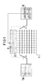
- the device for producing a test-compatible, largely fault-tolerant configuration for redundantly implemented systolic VLSI systems includes a VLSI system V consisting of the total number N 'arranged in rows and columns, a clock sequence control TC, a test bit generator TBG, and an evaluation unit AE and a selector bit generator SG.
- the clock sequence control TC which controls the sequence of the entire test process, outputs a set of selector bits via the selector bit generator SG, and finally switches the modules for the test process on or off line by line, is on the one hand with the selector bit generator SG, and on the other hand with lines that are not shown Control inputs on the VLSI system, which are indicated in FIG.
- the test bit generator TBG for supplying the input variables is connected line by line to the inputs of the VLSI system V, while the evaluation unit is connected line by line to the outputs of the VLSI system to check the result of the arithmetic operations carried out from the input variables.
- the process for producing a test-compatible, largely fault-tolerant configuration for redundantly implemented systolic VLSI systems initially provides for line-by-line testing of the individual modules. With the help of the selector bit generator SG and "Enable" signals at the control inputs of the VLSI system V, the individual modules are switched in a row in accordance with the 0/1 assignment of selector bits. In the given case, 8 out of 10 modules remain in operation line by line. After activating the individual modules, the A and B input variables are first created for the first line at the inputs of the VLSI system.
- the results of the arithmetic operation carried out are tapped line by line at the outputs of the VLSI system and fed to an evaluation unit AE.
- a new 0/1 assignment of selector bits is generated for the line from the selector bit generator SG and a new selection of in this case 8 out of 10 modules is selected for performing the arithmetic operations.
- This test process is repeated until either all 45 possibilities of an 8 out of 10 configuration of the modules have been tested in one line, or until a configuration has been found which gives a positive result in the computing operations carried out. If this is the case, the selector bits used for this are stored in the control logic, which is explained in FIG. 5.
- the modules in the second, third and all further lines of the VLSI system are then tested by performing the above-mentioned method steps.
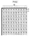
- FIG. 2 shows the arrangement of the modules M in columns and rows within a VLSI system according to the invention.
- the interconnection of the individual modules M with one another is not shown here for the sake of simplicity. It can be seen that each module M is assigned a control logic SL which serves to activate the switches of the corresponding module M.
- the control logic circuits of the modules of a column are each operated by a common selector bit input, while the activation of the modules line by line by supplying an "enable” signal (not shown here), which is supplied to each control logic together in one line.
- This "enable" signal and the 0/1 assignment of the selector bits at the selector bit inputs SBE make it possible to test the modules line by line.
- the regularity of the systolic field requires the control logic to be interconnected, so that one control logic of a module is connected to four other control logic that are in the immediate vicinity of the same. This does not apply to the control logic that is on the periphery of the VLSI system.
- the neighboring control logics are replaced by interconnecting the peripheral control logics with fixed 0 or 1 logic levels. This is indicated in FIG. 2 by the connection of the peripheral control logic with the outer bar boundary, and is explained in more detail in FIG. 5.
- FIG. 3 shows the input variables which are fed to the VLSI system during normal operation with a matrix-matrix multiplication.
- the input variables for the remaining modules in the remaining lines are analogous. For the configuration procedure, it is most sensible to select the input variables for each module in order to test the modules in order to be able to carry out a quick and simple check for a positive or negative result after the arithmetic operations have been carried out.
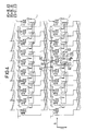
- FIG. 4 shows the interconnection of the modules, the illustration of which was omitted in FIG. 2 due to the clarity.
- the interconnection of the module M jk is given here as a representative of the interconnection of the other modules in the rows and columns of the VLSI system.
- the module M jk is connected at one input via a register R1 to 5 B switches BS, at another input via a register R2 to three A switches and at the output above the switch S to two output registers R3 and R4 connected in series.
- the A switches AS, B switches BS and C switches CS are located in front of the registers.
- the A and C switches establish connections between the modules in the row, while the B switches BS are responsible for connecting the modules in columns.
- a connection which is connected on the one hand between the register R1 and the input of the module M jk belonging to the register R1, on the other hand connects five further B switches of the module in the next lower j + 1 th line. These B switches are arranged in the j + 1-th row in the k-2-th, k-1-th, k, k + 1-th and k + 2-th column. Likewise, the connects B-switch BS of the module M jk five further modules are located in the next higher j-1 th row, each of which is in the k-2 th, k-1 th, k, k + 1 th and k + 2 -th column.
- a further connecting line which is connected between register R2 and the input of module M jk belonging to register R2, on the other hand connects the A switches of the modules on the right and the next but one on the right, which are in the k + 1-th and k + 2 -th column of the same row.
- the A-switches AS which are connected upstream of the register R2, enable a connection either to the input of the module on the left in the same line, to which a further register is assigned analogously to the register R1, in the k-1 th column, and a connection with the A switches of the modules in the k-2-th and k-3-th column of the same row.
- a connection to the A switches of the modules in the k + 1-th and k + 2-th column of the same line is made possible.
- the output of the module M jk is switched via a switch S to two output registers R3 and R4 which are connected in series, the output of the output register R4 being a connection to further C switches of the modules on the right and the next but one in the k + 1-th and Allows k + 2nd column of the same row.
- the switch S optionally switches the output of the module M jk or one of the three C switches CS of the module M jk to the output register R3.
- the C switch CS continues to connect the output register R3 via the switch S optionally to the two output registers of the modules connected in series, which are in the same row, but k-3rd, k-2nd and k-1st column are arranged.
- the A switch AS and the C switch CS of the module M jk are switched synchronously, ie the A switch AS provides a connection between the register R2 of the module M jk to the input belonging to the register R2 in the k-1- ten column and the same row arranged module, so the C switch via the switch S connects with the output register R3 of the module M jk to the two series-connected output registers of the module arranged in the k-1 th column and the same row. This applies to the remaining two switches of the A switch AS and C switch CS.
- FIG. 5 shows the control logic, which is split into a fault-tolerant part SLFI and a fault-tolerant part SLF.
- the A, B and C switches AS, BS, CS of the relevant module M jk are controlled.
- a total of ten logic variables must be made available to the control logic.
- the horizontal control line string is four bits wide and includes the logical variables Z j, k-1 , C j, k-1 , D j, k-1 and E j, k-1 or Z j, k , C j, k , D j, k and E j, k ;
- the vertical control line string is six bits wide and results from the logical variables C j, k , E j-1, k-1 , D j-1, k-1 , C j-1, k-1 , C j-1, k and C j-1, k + 1 and C j + 1, k , E j, k-1 , D j, k-1 , C j, k-1 , C j, k and C j, k + 1 .
- the local control logic is implemented redundantly. This is only possible with skillful assignment of the A, B and C switches AS, BS, CS, in that the control logic acts on the module M jk via the switches. Then an error in the control logic only affects the module M jk .
- the part of the control logic SLFI that passes the horizontal information on to the rest of the line is not fault-tolerant, because an error would be adopted by all the remaining modules.
- the control logic SLF that processes the vertical information is fault-tolerant, because incorrect information is only carried up to the module of the next line and can be reconfigured there.
- the fault-tolerant part of the control logic SLF is five times larger than the fault-tolerant part SLFI.
- the horizontal control line string which passes the information on to the rest of the line, is four bits wide and contains three control lines which contain the logic output variables Z j, k , D j, k and E j, k deliver, and are generated from the fault-intolerant part SLFI of the control logic.
- a fourth logical variable C j, k is obtained from the vertical control line via a latch L in the fault-tolerant control logic part.
- the vertical control wiring harness which passes the information on to modules in the next line, is six bits wide and consists of the logical variables D j, k-1 , E j, k-1 , C j, k-1 , C j, k , C j + 1, k and C j, k + 1 .
- the first four logical variables are generated directly from the corresponding logical input variables, while the last two logical variables are taken from neighboring control logics.
- the logical variable C j, k is applied to all control logic of the kth line, at the same time it forms part of the selector bit inputs SBE from FIG. 2. Furthermore, to activate the control logic located in a specific line, the fault-tolerant part SLF is additionally activated -Signal EN or EN 'supplied respectively for the j-th and j + 1-th line. Since one "Enable" signal is assigned to each line for the control logic, there is a total of eight “Enable” signals for the entire VLSI system. With the help of the logical input variables C j, k and the "Enable” signals, it is possible to activate or deactivate each individual module in the VLSI system during the configuration algorithm.
- FIG. 5 A circuit at gate level for the control logic according to FIG. 5 is shown in FIG.
- the ten logical input variables for the control logic are C j, k , E j, k-1 , D j, k-1 , C j, k-1 , Z j, k-1 , C j-1, k + 1 , C j-1, k , E j-1 , k-1 , D j -1 , k-1 and C j-1, k-1 .
- the logic output variables of the control logic are as follows: C j, k , E j, k , D j, k , Z j, k , D j, k , E j, k .
- the interconnection of the eight NAND gates, fifteen inverters and a NOR gate is as follows:
- the logical input variable C j, k forms a logical output variable C j, k on the one hand, and on the other hand it has a first input of a first NAND -Gatters N1 switched, a second logical input variable E j, k-1 is connected to a second input of the first NAND gate N1 and to a first input of a first NOR gate NO1.
- the logic input variable C j, k is connected to the second input of the first NOR gate NO1, and the logic input variable D j, k-1 is connected to the first input of a second NAND gate N2.
- An output of the first NAND gate N1 is connected to a first input of a third NAND gate N3 and the logic input variable C j, k is connected via a first inverter I1 to a first input of a fourth NAND gate N4.
- An output of the first NAND gate N1 supplies the logic output variable via a second inverter I2 E j, k .
- An output of the first NOR gate NO1 is connected via a third inverter I3 to the second input of the second NAND gate N2 and an output of the second NAND gate N2 via a fourth inverter I4 is on the one hand connected to a second input of the third NAND gate N2.
- Gate N3 connected and on the other hand supplies the logical output variable D j, k .
- the logical input variable C j, k-1 is connected via a fifth inverter I5 to a second input of the fourth NAND gate N4 and an output of the fourth NAND gate N4 via a sixth inverter I6 provides the logical output variable Z j, k .
- the output of the second NAND gate N2 provides the logic output variable D j, k and an output of the third NAND gate N3 supplies the logic output variable E j, k via a seventh inverter I7. D j, k .
- the logical input variable C j, k-1 results on the one hand in the logical output variable C j, k-1 and on the other hand provides an eighth Inverter I8 the logical output variable C j, k-1 .
- the logical input variable Z j, k-1 on the one hand forms the logical output variable Z j, k-1 and also supplies the logical output variable via a ninth inverter I9 Z j, k-1 .
- the logical input variable C j-1, k + 1 results in the output variable C j-1, k + 1 and supplies the negated output variable via a tenth inverter I10 C j-1, k + 1 .
- the logical input variable C j-1, k also results in the logical output variable C j-1, k and is connected to a first input of a fifth NAND gate N5 and to a first input of a second NOR gate NO2.
- the logical input variable E j-1, k-1 is connected on the one hand to the second input of the fifth NAND gate N5 and on the other hand to a second input of the second NOR gate NO2, the output of the fifth NAND gate N5 supplies the logic output variable via an eleventh inverter I11 E j-1, k .
- the output of the second NOR gate NO2 is connected to a sixth NAND gate N6 via a twelfth inverter I12, wherein the logic output variable D j-1, k can be tapped at the output of the sixth NAND gate N6 and can be tapped via a 13th Inverter I13 the logical output variable D j-1, k delivers.
- the output of the fifth NAND gate N5 and the output of the 13th inverter I13 are each connected to an input of a seventh NAND gate N7 and the output of the seventh NAND gate N7 is connected to a 14th inverter I14, the output of which logical output variable E j-1, k . D j-1, k can be tapped.
- the logical input variable D j-1, k-1 is connected on the one hand to a second input of the sixth NAND gate N6 and, on the other hand, to a first input of an eighth NAND gate N8 and the logic input variable E j-1, k-1 corresponds to the logical output variable E j-1, k-1 and can be tapped via a 16th inverter I16 as a logic output variable E j-1, k-1 .
- the output of the 16th inverter I16 is connected to a second input of the eighth NAND gate N8 and the output of the eighth NAND gate N8 is coupled to a 15th inverter I15, at whose output the logic output variable E j-1, k- 1st D j-1, k-1 tapped can be.
- the logical input variable C j-1, k-1 also forms the logical output variable C j-1, k-1 .
- Figures 7a to d give the error configurations that activate the switch B1, as well as their gate implementation of the associated logical equation. at.
- the switch B1 establishes a connection between the module M j-1, k and the module M j, k , ie a connection between two modules that are located in the k-th column and in each case in the j-th and j-1- line.
- the prerequisite for this is that both modules are functional.
- the connecting lines between the modules according to FIGS. 7a to 7c indicate that these modules take part in the arithmetic operations, for example matrix-matrix multiplication, and are functional, while those modules which are represented by black-filled squares in FIGS.
- the switch B1 establishes the connection between a module M j, k and a module M j-1, k in the k-th column, for example, that means both modules in the k-th column that lying horizontally to each other take part in the arithmetic operations, for example the matrix-matrix multiplication.
- B1 C j-1, k . C j, k . ( E j-1, k . E j, k ) + (E j-1, k . E j, k . D j-1, k . D j, k ) + (D j-1, k . D j, k )).
- the B1 switch is constructed by a total of six NAND gates N9, N10, N11, N12, N13 and N1 'and by two inverters I17 and I18.
- the logical output variables from the control logic in accordance with FIG. 6 are each connected to the inputs of the NAND gates N9, N10, N11, N12 and N13.
- the logical output variable E j, k as well as the logical output variable E j-1, k is applied to an input of the ninth NAND gate N9, the logic output variables E j, k . D j, k as well as the logical output variables E j-1, k .
- D j-1, k are each connected to an input of the NAND gate N10 and finally the logic output variables D j, k and D j-1, k are applied to inputs of the NAND gate N11.
- the outputs of the ninth NAND gate N9, the tenth NAND gate N10 and the eleventh NAND gate N11 are each switched to an input of a three-input NAND gate N1 ', the output of which is present at an input of the NAND gate N12 .
- the second input of the NAND gate N12 is connected to the logic output variable C j-1, k , while the output of the twelfth NAND gate N12 is connected to an input of the 13th NAND gate N13 via a 17th inverter I17.
- the second input of the thirteenth NAND gate N13 is connected to the logic output variable C j, k and the output signal for the B1 switch can be tapped off at the output of the 13th NAND gate N13 via an 18th inverter I18.
- FIGS. 8a to 8c indicate the error configurations which activate the switch B2 and the implementation at the gate level for its control. Faulty or defective modules are again identified by black squares in FIGS. 8a and 8b.
- the B2 switch establishes a connection from modules M j-1, k + 1 with modules M j, k . This means a connection, for example between a module of the j-1 th row and k + 1 th column to a module in the j th row of j-th row and k-th column k-th column.
- the prerequisite is that both modules are functional. It can be seen from FIG. 8a that exactly one defective module occurs in the j-1 th line up to the k th column, while in FIG.
- B2 C j, k . C j-1, k-1 . ((E j-1, k . D j-1, k ) + (E j, k . D j-1, k . D j, k )).
- FIG. 8 c An implementation according to this logical definition of the B2 switch is shown in Figure 8 c. It consists of a total of five NAND gates N14, N15, N16, N17 and N18 and two inverters I19 and I20.
- the logic output variables from the control logic according to FIG. 6 are switched again to inputs of these NAND gates.
- the logical output variables E j, k . D j, k as well as the logic output variable D j-1, k if each on inputs of the 14th NAND gate N14 and the logic output variables from the control logic E j, k and the logic output variable E j-1, k . D j-1, k each connected to inputs of the 15th NAND gate N15.
- the outputs of the 14th NAND gate N14 and the 15th NAND gate N15 are each switched to inputs of the 16th NAND gate N16. Its output is in turn connected to an input of the 17th NAND gate N17.
- the second input of the 17th NAND gate N17 is connected to the logic output variable C j-1, k + 1 and the output of the 17th NAND gate N17 via a 19th inverter I19 with an input of the 18th NAND gate N18 connected.
- the second input of this 18th NAND gate is again with a Logical output variables C j, k connected and the output of the 18th NAND gate forms the output of the B2 switch via the 20th inverter I20.
- FIGS. 9a and 9b Error configurations which activate the switch B3 are shown in FIGS. 9a and 9b and a realization of their activation at gate level is shown in FIG. 9c.
- the switch B3 establishes a connection between a module M j-1, k + 2 to a module M j, k .
- the prerequisite for this is again that these modules are functional.
- FIGS. 9a and 9b shows that exactly two malfunctioning or defective modules occur in each of the two figures in the j-1 th line.
- Switch B3 is activated precisely when the number of defective modules in the j-1 th row to the k + 1 th row column is just 2. Faulty modules are again identified by black squares in FIGS. 9a and 9b.
- B3 C j, k . E j, k . (D j-1, k + C j-1, k + 1 . E j-1, k . D j-1, k )).
- FIG. 9c The implementation of this logical definition by four NAND gates N19, N20, N21 and N22 and by two inverters I21 and I22 is shown in FIG. 9c.
- Logical output variables from the control logic according to FIG. 6 are in turn connected to the four NAND gates.
- D j-1, k are each switched to inputs of the 19th NAND gate N19, the output of which is connected to an input of the 20th NAND gate N20.
- a second input of the 20th NAND gate N20 is assigned the logic output variable D j-1, k busy.
- the output of the 20th NAND gate N20 is connected to an input of the 21st NAND gate N21, the second input of which is the logic input variable E j, k lies on.
- the output of the 21st NAND gate N21 is via an In verter I21 connected to an input of the 22nd NAND gate N22.
- the logic output variable C j, k is switched to the second input of the 22nd NAND gate N22 and the output of the 22nd NAND gate N22 forms the output of the B3 switch via the inverter I22.
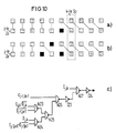
- FIGS. 10a and 10b indicate the error configuration which activate the switch B4 and FIG. 10c shows an implementation of its activation at the gate level.
- the switch B4 establishes a connection between a module M j-1, k-1 and a module M j, k . This means a connection between a module from the j-1 th row and k-1 th column to a module in the j th row j-th ze and k-th column k-th column. that both modules are functional.
- a comparison between FIGS. 10a and 10b shows that in each case there is one more inoperable module in the jth row than in the jth row.
- the switch B4 is then activated when the difference in the number of inoperable modules between the j-th and j-1-th rows up to the k-1-th column, including even 1. Faulty modules are identified by black squares, as in FIGS. 7 to 9.
- B4 C j-1, k-1 . C j, k . (( E j-1, k-1 . E j, k . D j, k ) + (E j-1, k-1 . D j-1, k-1 . D j, k )).
- FIG. 10c The implementation of this logical definition is shown in FIG. 10c. It contains five NAND gates N23, N24, N25, N26 and N27 as well as two inverters I23 and I24.
- the logic output variables of the control logic according to FIG. 6 are in turn connected to the NAND inputs, with the logic output variable D j, k and the output variable E j-1, k-1 .
- D j-1, k-1 each to an input of the 24th NAND gate and the logic output variable E j, k .
- D j, k such as E j-1, k-1 are connected to one input of the 23rd NAND gate.
- the output of the 23rd NAND gate N23 and the 24th NAND gate N24 is in each case connected to an input of the 25th NAND gate N25 and an output of the 25th NAND gate is connected to an input of the 26th NAND gate N26.
- Another input of the NAND gate N26 is assigned the logic output variable C j-1, k-1 and the output of the 26th NAND gate is connected via a 23rd inverter I23 to an input of the 27th NAND gate N27.
- the logic output variable C j, k is connected to a further input of the NAND gate N27, the output of the NAND gate N27 forms the output of the switch B4 via an inverter I24.
- FIGS. 11a and 11b show error configurations which activate the last of the B switches B5, and FIG. 11c shows an implementation at gate level for actuating the switch B5.
- the switch B5 establishes a connection between a module M j-1, k-2 and a module M j, k , ie between a module in the j-1 th row and k-2 th column and a module in FIG j-th row j-th row and k-th column k-th column.
- the prerequisite for this is that the module M j, k is functional.
- 11a and 11b shows that two faulty modules occur in each case in the jth line, of which, however, two faulty modules follow one behind the other in one line in FIG. 11a and in the jth line in FIG. 11b there is at least one functional module between each defective module.
- a faulty module occurs in the j-1 th row and k-1 th column, and in FIG. 11 b in the j-1 th row and k th column.
- the switch B5 is activated precisely when there are no faulty modules in the j-1st row up to the k-2nd column and in the jth row up to the kth column two inoperative modules.
- B5 C j, k . D j, k . ( E j-1, k-1 + (E j-1, k-1 . D j-1, k-1 . C j-1, k-1 )).
- FIG. 11c A realization of this logical definition at gate level by four NAND gates N28, N29, N30 and N31 and by three inverters I25, I26 and I27 is shown in FIG. 11c.
- the logic output variable C j-1, k-1 is fed via a 25th inverter I25 to an input of the 28th NAND gate N28, at the second input of which the logic output variable E j-1, k-1 .
- D j-1, k-1 connected.
- the output of the NAND gate N28 is connected to an input of the 29th NAND gate N29, to the second input of which the logic output variable E j-1, k-1 is applied.
- the output of the 29th NAND gate is connected to an input of the 30th NAND gate N30, the second input of which is occupied by the logic output variable D j, k .
- the output of the NAND gate N30 is connected via a 26th inverter I26 to the 31st NAND gate N31, to the second input of which the logic output variable C j, k is connected.
- the output of the NAND gate N31 is passed through a 27th inverter I27 and forms the output of the switch B5.
- FIG. 1 The implementation for controlling the three A and three C switches, which each have the same control logic, is shown in FIG.
- a realization of these logical equations is made possible by three NAND gates N32, N2 ', N3' and three inverters I28, I29 and I30.
- the logical output variable C j, k and C j, k-1 are each connected to an input of the 32nd NAND gate N32 and the logical output variable C j, k is also connected to an input of the three-input NAND gate N2 ' and connected to an input of the three-input NAND gate N3 '.
- the logical output variables are also connected to the NAND gate N2 ' C j, k-1 and Z j, k-1 and to the NAND gate N3 'the logic output variables C j, k-1 and Z j, k-1 .
- the Outputs of the three NAND gates are each passed through an inverter, so that the output of the 32nd NAND gate via a 28th inverter I28 forms a first output for driving the A1 or C1 switch and the output of the NAND gate N2 'via a 29th inverter I29 the second output for controlling the A2 or C2 switch.
- the output of the NAND gate N3 ' is also connected via a 30th inverter I30 and forms the third output for controlling the A3 or. C3 switch.
Landscapes
- Engineering & Computer Science (AREA)
- General Engineering & Computer Science (AREA)
- Physics & Mathematics (AREA)
- General Physics & Mathematics (AREA)
- Computer Hardware Design (AREA)
- Theoretical Computer Science (AREA)
- Computing Systems (AREA)
- Hardware Redundancy (AREA)
- Tests Of Electronic Circuits (AREA)
- Semiconductor Integrated Circuits (AREA)
- Design And Manufacture Of Integrated Circuits (AREA)
Abstract
Description
- Eine großflächige fehlertolerante VLSI-Integration, wie beispielsweise die LAI (Large Area Integration) oder WSI (Wafer Scale Integration), ist ein Beitrag zur Integration von Systemen mit einer sehr hohen Anzahl von über 10⁶ Transistoren. Diese Systeme können in bewährter CMOS-Technologie entworfen werden und erreichen heute schon Größenordnungen, welche erst mit zukünftiger Submikrontechnologie verfügbar sind (siehe hierzu Veröffentlichung von Dr. Ramacher "A Cost Oriented Redundancy Model For Defect-Tolerant VLSI/WSI-Systems, Adam Hilger, Proc. of the workshop on the designing for yield, Jan. 1988). Konfigurationsalgorithmen und Konfigurationsprozeduren haben hierbei die Aufgabe, aus einer Menge von redundant implementierten Funktionsmodulen eine Untermenge von funktionierenden Modulen ausfindig zu machen und Verbindungen zu aktivieren, so daß eine vorgegebene Funktion (beispielsweise ein Algorithmus oder eine Folge von Befehlen) auf der konfigurierten Menge ablauffähig ist. Eine Voraussetzung für redundante Implementation liegt darin, daß sie nur in solchen Systemen realisiert werden können, deren Architektur ein hohes Maß an Regularität aufweist. Systolische Felder sind hier sehr gut geeignet. Ein Algorithmus, welcher die Abbildung auf ein zweidimensionales systolisches Feld erlaubt, ist beispielsweise eine Matrix-Matrix-Multiplikation. Für eine großflächige monolithische Integration sind anzustreben:
- a) Fehlertoleranz, d.h. in der Hardware-Realisierung der Konfigurationsprozedur auftretende Effekte verhindern nicht eine Konfigurierbarkeit des Gesamtsystems,
- b) Testkompatibilität, d.h. der für nicht redundanten Entwurf nötige Systemtest ist ohne Mehraufwand an Hardware verwendbar für das redundant implementierte System, deckt die beschriebenen Defekte auf und aktiviert eine neue Konfiguration,
- c) ein minimaler Hardwarebedarf.
- Für eindimensionale Felder ist ein effektiver Algorithmus bei Aubusson und Catt "Wafer Scale Integration-Fault-Tolerant Procedure" in IEEE J. Solid State, Vol. SC-13, No. 3, June 1978, beschrieben. Andere Veröffentlichungen sind unter den Verfassern J.H. Kim, S. M. Reddy "On the design of easily testable and reconfigurable VLSI processor arrays", Workshop on designing for Yield, Oxford 1987, angeführt, die jedoch die Forderungen nach a) Testkompatibilität und b) Fehlertoleranz und c) minimaler Hardwareaufwand nur sehr eingeschränkt erfüllen. In der Veröffentlichung "Reconfiguration Architectures for VLSI Processing Arrays" Proc. of IEEE, May, 1986, S. 712-722 von M. Sami and R. Steffanelli sind großflächige monolithische Integrationen beschrieben, die jedoch alle drei Forderungen Fehlertoleranz, Testkompatibilität und minimaler Hardwarebedarf überhaupt nicht erfüllen.
- Systolische Felder sind aufgrund ihrer Regularität sehr gut geeignet für einen redundanten Systementwurf. Ein effektiver Konfigurationsalgorithmus, jedoch nur für eindimensionale systolische Felder, ist in der bereits genannten Veröffentlichung von Aubusson und Catt beschrieben. Eine Konfigurationsprozedur für zweidimensionale systolische Felder, welche die Eigenschaften a) Fehlertoleranz, b) Testkompatibilität und c) minimaler Hardwarebedarf aufweisen, können aus dieser Veröffentlichung jedoch nicht abgeleitet werden.
- Der Erfindung liegt die Aufgabe zugrunde, ein Verfahren und eine Vorrichtung zur Konfiguration für redundant implementierte systolische VLSI-Systeme anzugeben, die die Bedingungen a) Fehlertoleranz, b) Testkompatibilität und c) minimaler Hardwarebedarf erfüllen.
- Diese Aufgabe wird erfindungsgemäß für das Verfahren durch die im kennzeichnenden Teil des ersten Patentanspruchs angegebenen Merkmale und für die Vorrichtung für die im sechsten Patentanspruch angegebenen kennzeichnenden Merkmale gelöst.
- Weitere Ausgestaltungen der Erfindung, insbesondere der Aufbau des VLSI-Systems, sind in den Unteransprüchen angegeben und werden dort näher erläutert.
- Da das Verfahren zur Konfiguration des VLSI-Systems (Konfigurationsalgorithmus) sich auf eine Matrix-Matrix-Multiplikation bezieht, ergibt sich als Vorzug, daß die einzelnen Module des systolischen Feldes von einer einfachen Struktur sind, dennoch lassen sich hier in voller Allgemeinheit diejenigen Probleme erkennen, welche mit Konfiguration und Test systolischer Felder einhergehen. Der hier vorgestellte Konfigurationsalgorithmus ist deshalb ohne Einschränkung übertragbar, beispielsweise auf ein zweidimensionales Feld von RISC-Prozessoren. Der Entwurf eine solchen LAI/WSI-Systems kann sich dann konzentrieren auf die systolische Abbildung einer genügend großen Menge von Algorithmen aus dem Bereich der allgemeinen und intelligenten Musterverarbeitung (Sprach- und Bildverarbeitung).
- Ein Ausführungsbeispiel der Erfindung ist in den Zeichnungen dargestellt und wird im folgenden näher beschrieben. Es zeigen:
- Figur 1 die Anordnung zur Durchführung des Konfigurationsalgorithmus für ein redundant implementiertes systolisches VLSI-System,
- Figur 2 eine Anordnung des erfindungsgemäßen VLSI-Systems zur Durchführung einer Matrix-Matrix-Multiplikation,
- Figur 3 die Eingabe der Eingangsvariablen zur Matrix-Matrix-Multiplikation,
- Figur 4 eine Verschaltung der einzelnen Module untereinander im erfindungsgemäßen VLSI-System,
- Figur 5 ein Blockschaltbild der zu jedem Modul gehörenden Steuerlogik, zur Ansteuerung der A-, B-, C-Schalter eines jeden Moduls,
- Figur 6 eine Schaltung auf Gatterebene für die Steuerlogik nach Figur 5,
- Figur 7a bis c Fehlerkonfigurationen, welche den Schalter B1 aktivieren,
- Figur 7d Schaltungsrealisierung auf Gatterebene für die Ansteuerung des Schalters B1,
- Figur 8a, b Fehlerkonfigurationen, welche den Schalter B2 aktivieren,
- Figur 8c Schaltungsrealisierung auf Gatterebene für die Ansteuerung des Schalters B2,
- Figur 9a, b Fehlerkonfigurationen, welche den Schalter B3 aktivieren,
- Figur 9c Schaltungsrealisierung auf Gatterebene für die Ansteuerung des Schalters B3,
- Figur 10a, b Fehlerkonfiguration, welche den Schalter B4 aktivieren,
- Figur 10c Schaltungsrealisierung auf Gatterebene für die Ansteuerung des Schalters B4,
- Figur 11a, b Fehlerkonfigurationen, welche den Schalter B5 aktivieren,
- Figur 11c Schaltungsrealisierung auf Gatterebene für die Ansteuerung des Schalters B5,
- Figur 12 Gatterrealisierung für die Ansteuerung der Schalter A bzw. C.
- Die Vorrichtung zur Herstellung einer testkompatiblen, weitgehend fehlertoleranten Konfiguration für redundant implementierte systolische VLSI-Systeme beinhaltet nach Figur 1 ein aus der Gesamtzahl N′ in Zeilen und Spalten angeordnete Module bestehendes VLSI-System V, eine Taktablaufsteuerung TC, einen Testbitgenerator TBG, eine Auswerteeinheit AE und einen Selektorbitgenerator SG. Die Taktablaufsteuerung TC, die den Ablauf des gesamten Testvorgangs steuert, einen Satz von Selektorbits über den Selektorbitgenerator SG ausgibt, und schließlich zeilenweise die Module für den Testvorgang ein- bzw. ausschaltet, ist zum einen mit dem Selektorbitgenerator SG, zum anderen zeilenweise mit nicht eingezeichneten Steuereingängen auf dem VLSI-System, der in der Figur 1 durch Schalter an beiden Seiten des Systems angedeutet sind und in Figur 5 näher erläutert werden, verbunden. Je ein Selektorbit schaltet dabei die Module in einer Spalte des VLSI-Systems entsprechend seiner 0/1-Belegung ein oder aus und mit Hilfe von "Enable"-Signalen an den Steuereingängen des VLSI-Systems werden die Module in der gewünschten Zeile aktiviert. Der Testbitgenerator TBG zur Lieferung der Eingangsvariablen ist zeilenweise mit den Eingängen des VLSI-Systems V verbunden, während die Auswerteeinheit zur Prüfung des Ergebnisses der ausgeführten Rechenoperationen aus den Eingangsvariablen zeilenweise mit den Ausgängen des VLSI-Systems verschaltet ist.
- Die Größe des hier verwendeten VLSI-Systems beträgt 8x10 Module, wobei die vorgesehene Matrix-Matrix-Multiplikation lediglich 8 x 8 Module benötigt. Um eine bestimmt Anzahl, in diesem Falle 8, von funktionierenden Modulen aus einer großen Anzahl von in diesem Falle 10 redundant implementierten Modulen zu einem gewünschten System zusammenzubinden, bedarf es zweier Schritte:
- a) des Aufbaus eines Leitungsnetzes für Ausgangsdaten für jede beliebige Kombination von 8 aus 10 Modulen,
- b) des Tests jedes solchen Aufbaus durch Eingabe von Testmustern repräsentiert durch logische Eingangsvariablen aus dem Testbitgenerator und Auswertung der Ausgangsmuster repräsentiert durch Ausgangsvariablen in der Auswerteeinheit AE.
- Das Verfahren zur Herstellung einer testkompatiblen, weitgehend fehlertoleranten Konfiguration für redundant implementierte systolische VLSI-Systeme sieht zunächst das zeilenweise Prüfen der einzelnen Module vor. Mit Hilfe des Selektorbitgenerators SG und "Enable"-Signalen an den Steuereingängen des VLSI-Systems V werden die einzelnen Module in einer Zeile entsprechend der 0/1-Belegung von Selektorbits funktionsfähig oder funktionsunfähig geschaltet. Im vorgegebenen Fall bleiben dabei jeweils zeilenweise 8 von 10 Modulen in Betrieb. Nach Aktivierung der einzelnen Module werden die A- und B-Eingangsvariablen zunächst für die erste Zeile an die Eingänge des VLSI-Systems angelegt.
- Die Ergebnisse der ausgeführten Rechenoperation, in diesem Fall eine Multiplikation der Eingangsvariablen, wird an den Ausgängen des VLSI-Systems jeweils zeilenweise abgegriffen und einer Auswerteeinheit AE zugeführt. Bei einem negativen Ergebnis der ausgeführten Rechenoperationen wird für die Zeile eine neue 0/1-Belegung von Selektorbits aus dem Selektorbitgenerator SG erzeugt und eine neue Auswahl von in diesem Falle 8 von 10 Modulen zur Durchführung der Rechenoperationen ausgewählt. Dieser Testvorgang wird so oft wiederholt, bis entweder alle 45 Möglichkeiten einer 8 aus 10-Konfiguration der Module in einer Zeile ausgetestet wurden, oder bis eine Konfiguration gefunden wurde, die ein positives Ergebnis bei den durchgeführten Rechenoperationen liefert. Ist dies der Fall, so werden die hierfür verwendeten Selektorbits in der Steuerlogik, die in Figur 5 erläutert wird, abgespeichert. Anschließend werden unter der Durchführung der obengenannten Verfahrensschritte die Module in der zweiten, dritten und allen weiteren Zeilen des VLSI-Systems ausgetestet.
- Bei den vorgesehenen Rechenoperationen handelt es sich um eine Matrix-Matrix-Multiplikation, die entsprechend definiert ist als ci,k =aij · bj,k , für i, k = 1 bis N, in diesem Falle stellen aij und bjk Eingangsvariablen und Cjk Ausgangsvariablen für die Rechenoperation dar. Zur Prüfung der Module in der ersten Zeile ergebeb sich hieraus für die Eingangsvariablen folgende Kombinationen:

a₁.b₁, a₁.b₂,...a₁.b₈
mit a₁ : = (a₁₁, a₁₂,...a₁₈),
b₁ : = (b₁₁, b₂₁,...b₈₁),
b₂ : = (b₁₂, b₂₂....b₈₂),
b₈ : = (b₁₈, b₂₈,...b₈₈).
Als Ausgangsvariable ergibt sich für die erste Zeile c₁ = (c₁₁, c₁₂,...c₁₈). - Figur 2 zeigt die spalten- und zeilenweise Anordnung der Module M innerhalb eines erfindungsgemäßen VLSI-Systems. Die Verschaltung der einzelnen Module M untereinander ist hierbei zur Vereinfachung nicht dargestellt. Man erkennt, daß jedem Modul M eine Steuerlogik SL zugeordnet ist, die zur Aktivierung der Schalter des entsprechenden Moduls M dient.
- Die Steuerlogikschaltungen der Module einer Spalte werden jeweils von einem gemeinsamen Selektorbiteingang bedient, während die Aktivierung der Module zeilenweise durch Zuführung eines hier nicht eingezeichneten "Enable"-Signals, welches jeder Steuerlogik in einer Zeile gemeinsam zugeführt wird. Durch dieses "Enable"-Signal und der 0/1-Belegung der Selektorbits an den Selektorbiteingängen SBE ist es möglich, die Module zeilenweise auszutesten. Die Regularität des systolischen Feldes erfordert eine Verschaltung der Steuerlogiken untereinander, so daß eine Steuerlogik eines Moduls mit je vier anderen Steuerlogiken, die sich in unmittelbarer Nachbarschaft derselben befinden, verbunden sind. Dies trifft nicht für die Steuerlogiken zu, die sich an der Peripherie des VLSI-Systems befinden. Hier werden die benachbarten Steuerlogiken ersetzt, durch ein Verschalten der peripheren Steuerlogiken mit fest vorgegebenen 0- oder 1-Logikpegeln. Dies ist in Figur 2 durch die Verbindung der peripheren Steuerlogiken mit der äußeren Balkenbegrenzung angedeutet, und wird in Figur 5 nochmals näher erläutert.
- Figur 3 zeigt die Eingangsvariablen, die während des normalen Betriebs bei einer Matrix-Matrix-Multiplikation dem VLSI-System zugeführt werden. Man erkennt, daß die Eingangs variablen jeder Zeile sowie jeder Spalte jeweils um einen Taktschritt verzögert angelegt werden. Die Zuführung der Eingangsvariablen für die Module in der ersten Zeile ergibt sich daher wie folgt:
Für das Modul in der ersten Spalte und ersten Zeile werden die Eingangsvariablen a₁ = (a₁₁, a₁₂,...a₁₈) sowie die Eingangsvariablen b₁ = (b₁₁, b₂₁,...b₈₁) zugeführt. Für das Modul in der zweiten Spalte der ersten Zeile ergeben sich die Eingangsvariablen a₁ = (a₁₁, a₁₂,...a₁₈) und b₂ = (b₁₂, b₂₂,...b₈₂). Für das Modul in der letzten Spalte der ersten Zeile ergibt sich für die Eingangsvariablen a₁ = (a₁₁, a₁₂,...a₁₈) sowie b₈ = ( b₁₈, b₂₈,...b₈₈). Analog ergeben sich die Eingangsvariablen für die restlichen Module in den übrigen Zeilen. Für die Konfigurationsprozedur ist es am sinnvollsten zum Testen der Module die Eingangsvariablen für jedes Modul gleich zu wählen, um nach den durchgeführten Rechenoperationen eine schnelle und einfache Überprüfung auf ein positives oder negatives Ergebnis durchführen zu können. - Figur 4 zeigt die Verschaltung der Module untereinander, deren Darstellung in Figur 2 aufgrund der Übersichtlichkeit entfiel. Die Verschaltung des Moduls Mjk wird hier stellvertretend für die Verschaltung der übrigen Module in den Zeilen und Spalten des VLSI-Systems angegeben. Das Modul Mjk ist an einem Eingang über ein Register R1 an 5 B-Schalter BS, an einem weiteren Eingang über ein Register R2 an drei A-Schalter und am Ausgang über dem Schalter S an zwei in Serie geschaltete Ausgangsregister R3 und R4 angeschlossen. Den Registern vorgelagert befinden sich jeweils die A-Schalter AS, B-Schalter BS und C-Schalter CS. Die A- und C-Schalter stellen Verbindungen der Module untereinander in der Zeile her, während die B-Schalter BS für eine spaltenweise Verschaltung der Module zuständig sind. Eine Verbindung, die einerseits zwischen dem Register R1 und dem zum Register R1 zugehörenden Eingang des Moduls Mjk angeschlossen ist, verbindet andererseits fünf weitere B-Schalter des Moduls in der nächsttieferen j+1-ten Zeile. Diese B-Schalter sind jeweils in der j+1-ten Zeile in der k-2-ten, k-1-ten, k, k+1-ten und k+2-ten Spalte angeordnet. Ebenso verbindet der B-Schalter BS des Moduls Mjk fünf weitere in der nächsthöheren j-1-ten Zeile liegen Module, die sich jeweils in der k-2-ten, k-1-ten, k, k+1-ten und k+2-ten Spalte befinden. Mit Hilfe dieser eingeführten "Bypässe", die durch die Verbindungsleitungen und die B-Schalter realisiert sind, ist es möglich, fehlerhafte Module in einer Spalte zu überbrücken. Eine weitere Verbindungsleitung, die zwischen dem Register R2 und dem zum Register R2 zugehörenden Eingang des Moduls Mjk angeschlossen ist, verbindet andererseits die A-Schalter der rechts und übernächsten rechts liegenden Module, die sich in der k+1-ten und k+2-ten Spalte derselben Zeile befinden. Die A-Schalter AS, die dem Register R2 vorgeschaltet sind, ermöglichen eine Verbindung wahlweise zum einen zum Eingang des in derselben Zeile links befindlichen Moduls, dem ein weiteres Register analog zum Register R1 zugeordnet ist, in der k-1-ten Spalte, sowie eine Verbindung mit den A-Schaltern der Module in der k-2-ten und k-3-ten Spalte derselben Zeile. Gleichzeitig wird eine Verbindung zu den A-Schaltern der Module in der k+1-ten und k+2-ten Spalte der gleichen Zeile ermöglicht. Der Ausgang des Moduls Mjk wird über einen Schalter S auf zwei in Serie geschaltete Ausgangsregister R3 und R4 geschaltet, wobei der Ausgang des Ausgangsregisters R4 eine Verbindung zu weiteren C-Schaltern der rechts und übernächsten rechts liegenden Module in der k+1-ten und k+2-ten Spalte derselben Zeile ermöglicht. Der Schalter S schaltet wahlweise den Ausgang des Moduls Mjk oder einen der drei C-Schalter CS des Moduls Mjk auf das Ausgangsregister R3. Der C-Schalter CS verbindet weiterhin über den Schalter S das Ausgangsregister R3 wahlweise mit dem in Serie geschalteten zwei Ausgangsregistern der Module, die in der gleichen Zeile, aber k-3-ten, k-2-ten und k-1-ten Spalte angeordnet sind. Gleichzeitig wird eine Verbindung zu den C-Schaltern der Module in der k+1-ten und k+2-ten Spalte der gleichen Zeile ermöglicht. Der A-Schalter AS und der C-Schalter CS des Moduls Mjk wird synchron geschaltet, d.h. stellt der A-Schalter AS eine Verbindung zwischen dem Register R2 des Moduls Mjk zu dem zum Register R2 zugehörenden Eingang des in der k-1-ten Spalte und der gleichen Zeile angeordneten Moduls her, so stellt der C-Schalter über den Schalter S eine Verbin dung mit dem Ausgangsregister R3 des Moduls Mjk zu den beiden in Serie geschalteten Ausgangsregistern des in der k-1-ten Spalte und der gleichen Zeile angeordneten Moduls her. Dies gilt übertragen für die verbleibenden restlichen zwei Schalter der A-Schalter AS und C-Schalter CS.
- Figur 5 zeigt die Steuerlogik, die in einen fehlerintoleranten Teil SLFI und einen fehlertoleranten Teil SLF aufgespalten ist. Mit Hilfe der Steuerlogik werden die A-, B- und C-Schalter AS, BS, CS des betreffenden Moduls Mjk gesteuert. Insgesamt müssen der Steuerlogik zehn logische Variablen zur Verfügung gestellt werden. Der horizontale Steuerleitungsstrang ist hierbei vier Bit breit und umfaßt die logischen Variablen Zj,k-1, Cj, k-1,
Dj, k-1 undEj, k-1 bzw. Zj, k, Cj, k,Dj, k undEj, k ; der vertikale Steuerleitungsstrang ist sechs Bit breit und ergibt sich aus den logischen Variablen Cj, k,Ej-1, k-1 ,Dj-1, k-1 , Cj-1, k-1, Cj-1, k und Cj-1, k+1 bzw. Cj+1, k,Ej, k-1 ,Dj, k-1 , Cj, k-1, Cj, k und Cj, k+1. Hierbei ergibt sich eine Definition der logischen Variablen wie folgt:
Cj,k = 0, wenn das Modul Mjk abgeschaltet ist,
= 1, wenn das Modul Mjk eingeschaltet ist,
Ej,k = 0, wenn ein Fehler in der Zeile j bis zur Spalte k einschließlich existiert,
= 1, wenn genau ein Fehler in der Zeile j bis zur Spalte k einschließlich existiert,
Dj,k = 0, wenn keine zwei Fehler in der Zeile j bis zur Spalte k einschließlich existieren,
= 1, wenn genau zwei Fehler in der Zeile j bis zur Spalte k einschließlich existieren,
Zj,k = 0, wenn höchstens eins der Module Mj,k-1 oder Mjk defekt ist,
= 1, wenn beide Module Mjk-1 und Mjk defekt sind. - Hierbei gilt immer, falls die logische Variable D = 1 ist, so ist ebenfalls die logische Variable E = 1, und falls die logi sche Variable E = 0 ist, so ist ebenfalls die logische Variable D = 0.
- Die lokale Steuerlogik wird redundant implementiert. Dies geht nur bei geschickter Zuordnung der A-, B- und C-Schalter AS, BS, CS, indem die Steuerlogik über die Schalter auf das Modul Mjk wirkt. Dann wirkt sich ein Fehler in der Steuerlogik nur auf das Modul Mjk aus. Der Teil der Steuerlogik SLFI, welche die horizontale Information an den Rest der Zeile weitergibt, ist nicht fehlertolerant, weil ein Fehler von allen restlichen Modulen übernommen würde. Dagegen ist die die vertikale Information verarbeitende Steuerlogik SLF fehlertolerant, weil eine Falschinformation nur bis zum Modul der nächsten Zeile getragen wird und dort neu konfiguriert werden kann. Der fehlertolerante Teil der Steuerlogik SLF ist fünfmal größer als der fehlerintolerante Teil SLFI. Der horizontale Steuerleitungsstrang, welcher die Information an den Rest der Zeile weitergibt, ist vier Bit breit und beinhaltet drei Steuer leitungen, die die logischen Ausgangsvariablen Zj,k ,
Dj, k undEj, k liefern, und aus dem fehlerintoleranten Teil SLFI der Steuerlogik generiert werden. Eine vierte logische Variable Cj, k wird hierbei aus dem vertikalen Steuerleitungsstrang über ein Latch L im fehlertoleranten Steuerlogikteil gewonnen. Der vertikale Steuerleitungsstrang, der die Informationen an Module in der nächsten Zeile weitergibt, ist sechs Bit breit und besteht aus den logischen VariablenDj, k-1 ,Ej, k-1 ,Cj, k-1 , Cj, k, Cj+1, k und Cj, k+1. Die ersten vier logischen Variablen werden direkt aus den entsprechenden logischen Eingangsvariablen erzeugt, während die letzten beiden logischen Variablen aus benachbarten Steuerlogiken entnommen werden. - Für die Steuerlogiken, die an der Peripherie des VLSI-Systems angeordnet sind, ergeben sich die Werte für die logischen Variablen durch folgende Anfangsbedingungen:
C0, k-1 = 1 für k = 1,...10;
E0, k-1 = 0, D0, k-1 = 0 für k = 1, ...10, C1, 0 = 1, D1, 0 = E1, 0 = 0; Z1, 0 = X (don't care), wobei diese logischen Variablen entsprechend den genannten Anfangsbedingungen fest verschaltet werden. - Die logische Variable Cj, k wird auf alle Steuerlogiken der k-ten Zeile aufgeschaltet, gleichzeitig bildet sie einen Teil der Selektorbiteingänge SBE aus Figur 2. Weiterhin wird zur Aktivierung der in einer bestimmten Zeile befindlichen Steuerlogik dem fehlertoleranten Teil SLF zusätzlich ein "Enable"-Signal EN bzw. EN′ jeweils für die j-te und j+1-te Zeile zugeführt. Da pro Zeile für die Steuerlogiken je ein "Enable"-Signal zugeordnet ist, ergibt sich für das gesamte VLSI-System eine Gesamtanzahl von acht "Enable"-Signalen. Mit Hilfe der logischen Eingangsvariablen Cj, k und der "Enable"-Signale ist es möglich, während des Konfigurationsalgorithmusses jedes einzelne Modul in dem VLSI-System zu aktivieren oder außer Betrieb zu setzen.
- Eine Schaltung auf Gatterebene für die Steuerlogik nach Figur 5 ist in der Figur 6 wiedergegeben. Um die A-, B-, C-Schalter eines jeden Moduls zu steuern, sind insgesamt 21 logische Variablen notwendig, die jedoch aus den zehn bereits in Figur 5 genannten logischen Eingangsvariablen für die Steuerlogik gewonnen werden können. Die zehn logischen Eingangsvariablen für die Steuerlogik sind Cj, k,
Ej, k-1 ,Dj, k-1 , Cj, k-1, Zj, k-1, Cj-1, k+1, Cj-1, k, Ej-1, k-1, Dj-1 ,k-1 und Cj-1, k-1. Die logischen Ausgangsvariablen der Steuerlogik, deren erste vier fehlerintolerante Ausgangsvariablen darstellen, lauten wie folgt: Cj, k,Ej, k ,Dj, k, Zj, k, Dj, k, Ej, k .Dj, k, Cj, k-1,Cj,k-1, Zj, k-1,Zj, k-1 , Cj-1, k+1,Cj-1, k+1 , Cj-1, k,Ej-1, k , Dj-1, k, Dj-1, k,Ej-1, k . Dj-1, kCj-1, k-1, Ej-1, k-1, Ej-1, k-1 und Ej-1, k-1 .
Dj-1, k-1 . Diese 21 logischen Ausgangsvariablen werden zur Ansteuerung der fünf B-Schalter nach Figur 7d, 8c, 9c, 10c und 11c sowie zur Ansteuerung der A- und C-Schalter nach Figur 12 eingesetzt. Der gestrichelte Teil der Schaltung nach Figur 6 stellt den fehlerintoleranten Teil der Steuerlogik dar, fehlerhafte Gatter oder Inverter in diesem Bereich bedingen Auswirkungen auf die restlichen Steuerlogiken der in der gleichen Zeile angeordneten Module. Ein Fehler in dem fehlertoleranten Teil der Schaltung nach Figur 6 oder in der Gatterlogik für die Steuervariablen zur Ansteuerung der A-, B-, C-Schalter hat keinerlei Auswirkungen auf andere Module und kann einfach durch eine Überbrückung des defekten Moduls mit seiner Steuereinheit umgangen werden. - Die Verschaltung der acht NAND-Gatter, fünfzehn Inverter und einem NOR-Gatter sieht im einzelnen wie folgt aus: Die logische Eingangsvariable Cj, k bildet zum einen logische Ausgangsvariable Cj, k, zum anderen ist sie mit einem ersten Eingang eines ersten NAND-Gatters N1 geschaltet, eine zweite logische Eingangsvariable
Ej, k-1 ist mit einem zweiten Eingang des ersten NAND-Gatters N1 und mit einem ersten Eingang eines ersten NOR-Gatters NO1 verschaltet. Die logische Eingangsvariable Cj, k ist an den zweiten Eingang des ersten NOR-Gatters NO1 angeschlossen, und die logische EingangsvariableDj, k-1 ist mit dem ersten Eingang eines zweiten NAND-Gatters N2 verschaltet. Ein Ausgang des ersten NAND-Gatters N1 ist mit einem ersten Eingang eines dritten NAND-Gatters N3 verbunden und die logische Eingangsvariable Cj, k ist über einen ersten Inverter I1 an einen ersten Eingang eines vierten NAND-Gatters N4 angeschlossen. Ein Ausgang des ersten NAND-Gatters N1 liefert über einen zweiten Inverter I2 die logische AusgangsvariableEj, k . Ein Ausgang des ersten NOR-Gatters NO1 ist über einen dritten Inverter I3 mit dem zweiten Eingang des zweiten NAND-GAtters N2 verschaltet und ein Ausgang des zweiten NAND-Gatters N2 über einen vierten Inverter I4 ist zum einen mit einem zweiten Eingang des dritten NAND-Gatters N3 verbunden und liefert zum anderen die logische AusgangsvariableDj, k . Die logische Eingangsvariable Cj, k-1 ist über einen fünften Inverter I5 mit einem zweiten Eingang des vierten NAND-Gatters N4 verbunden und ein Ausgang des vierten NAND-Gatters N4 über einen sechsten Inverter I6 liefert die logische Ausgangsvariable Zj, k. Der Ausgang des zweiten NAND-Gatters N2 liefert die logische Ausgangsvariable Dj, k und ein Ausgang des dritten NAND-Gatters N3 liefert über einen siebten Inverter I7 die logische Ausgangsvariable Ej, k.Dj, k . Die logische Eingangsvariable Cj, k-1 ergibt zum einen die logische Ausgangsvariable Cj, k-1 und liefert zum anderen über einen achten Inverter I8 die logische AusgangsvariableCj, k-1 . Die logische Eingangsvariable Zj, k-1 bildet zum einen die logische Ausgangsvariable Zj, k-1 und liefert weiterhin über einen neunten Inverter I9 die logische AusgangsvariableZj, k-1 . Ebenfalls ergibt die logische Eingangsvariable Cj-1, k+1 die Ausgangsvariable Cj-1, k+1 und liefert über einen zehnten Inverter I10 die negierte AusgangsvariableCj-1, k+1 . Die logische Eingangsvariable Cj-1, k ergibt weiterhin die logische Ausgangsvariable Cj-1, k und ist mit einem ersten Eingang eines fünften NAND-Gatters N5 und mit einem ersten Eingang eines zweiten NOR-Gatters NO2 verschaltet. Die logische EingangsvariableEj-1, k-1 ist zum einen mit dem zweiten Eingang des fünften NAND-Gatters N5 und zum anderen mit einem zweiten Eingang des zweiten NOR-Gatters NO2 angeschlossen, der Ausgang des fünften NAND-Gatters N5 liefert über einen elften Inverter I11 die logische AusgangsvariableEj-1, k . Der Ausgang des zweiten NOR-Gatters NO2 ist über einen zwölften Inverter I12 mit einem sechsten NAND-Gatter N6 verschaltet, wobei am Ausgang des sechsten NAND-Gatters N6 die logische Ausgangsvariable Dj-1, k abgegriffen werden kann und die über einen 13. Inverter I13 die logische AusgangsvariableDj-1, k liefert. Der Ausgang des fünften NAND-Gatters N5 und der Ausgang des 13. Inverters I13 werden jeweils auf einen Eingang eines siebten NAND-Gatters N7 geschaltet und der Ausgang des siebten NAND-Gatters N7 ist an einen 14. Inverter I14 angeschlossen, an dessen Ausgang die logische Ausgangsvariable Ej-1, k .Dj-1, k abgegriffen werden kann. Die logische EingangsvariableDj-1, k-1 ist zum einen mit einem zweiten Eingang des sechsten NAND-Gatters N6 und zum anderen an einen ersten Eingang eines achten NAND-Gatters N8 angeschlossen und die logische EingangsvariableEj-1, k-1 entspricht der logischen AusgangsvariablenEj-1, k-1 und ist über einen 16. Inverter I16 als logische Ausgangsvariable Ej-1, k-1 abgreifbar. Der Ausgang des 16. Inverters I16 ist mit einem zweiten Eingang des achten NAND-Gatters N8 verschaltet und der Ausgang des achten NAND-Gatters N8 ist auf einen 15. Inverter I15 angekoppelt, an dessem Ausgang die logische Ausgangsvariable Ej-1, k-1 .Dj-1, k-1 abgegriffen werden kann. Schließlich bildet die logische Eingangsvariable Cj-1, k-1 ebenfalls die logische Ausgangsvariable Cj-1, k-1. - In den nachfolgenden Figuren werden die Fehlerkonfigurationen beschrieben, welche die A-, B- oder C-Schalter aktivieren, ebenso die Realisierung der zugehörenden Ansteuerlogik. Der jeweilige Ausgang dieser Ansteuerlogik dient zur Aktivierung der entsprechenden Schalter über in den Figuren 7 bis 12 nicht dargestellte "transmission gates".
- Die Figuren 7a bis d geben die Fehlerkonfigurationen, welche den Schalter B1 aktivieren, sowie deren Gatterrealisation der zugehörenden logischen Gleichung. an. Der Schalter B1 stellt eine Verbindung des Moduls Mj-1, k mit dem Modul Mj, k her, d.h. eine Verbindung zwischen zwei Modulen, die sich in der k-ten Spalte und jeweils in der j-ten und j-1-ten Zeile befinden. Voraussetzung dafür ist, daß beide Module funktionsfähig sind. Die Verbindungslinien zwischen den Modulen nach den Figuren 7a bis 7c deuten an, daß diese Module an den Rechenoperationen, beispielsweise der Matrix-Matrix-Multiplikation teilnehmen und funktionsfähig sind, während solche Module, die in den Figuren 7a bis 7c durch scharz aufgefüllte Quadrate dargestellt sind, und keine Verbindungslinien zu übrigen Modulen aufweisen, defekte oder fehlerhafte Module darstellen. Man erkennt, daß in der Figur 7a kein solches funktionsunfähiges Modul vorhanden ist, im Gegensatz zu Figur 7b, wo pro Zeile je ein defektes Modul und nach Figur 7c je zwei defekte Module pro Zeile auftreten. Zur Aktivierung des B1-Schalters ist es nun wichtig, daß die Einzelfehler nach Figur 7b bzw. die Doppelfehler nach Figur 7c in beiden Zeilen bis zur k-ten Spalte aufgetreten sind. Ist dies der Fall, so stellt der Schalter B1 beispielsweise in der k-ten Spalte die Verbindung zwischen einem Modul Mj, k und einem Modul Mj-1, k her, dies bedeutet, beide Module in der k-ten Spalte, die horizontal zueinander liegen, nehmen an den Rechenoperationen, beispielsweise der Matrix-Matrix-Multiplikation teil.
- Die logische Definition der Steuervariablen für den B1-Schalter lautet:
B1 = Cj-1, k . Cj, k . (Ej-1, k .Ej, k ) + (Ej-1, k . Ej, k .Dj-1, k .Dj, k ) + (Dj-1, k . Dj, k)). - Eine solche Realisierung ist in der Figur 7d auf Gatterebene wiedergegeben. Der B1-Schalter wird durch insgesamt sechs NAND-Gatter N9, N10, N11, N12, N13 und N1′ sowie durch zwei Inverter I17 und I18 aufgebaut. Die logischen Ausgangsvariablen aus der Steuerlogik nach Figur 6 werden hier jeweils an die Eingänge der NAND-Gatter N9, N10, N11, N12 und N13 aufgeschaltet. Die logische Ausgangsvariable
Ej, k sowie die logische AusgangsvariableEj-1, k wird jeweils auf einen Eingang des neunten NAND-Gatters N9, die logischen Ausgangsvariablen Ej, k .Dj, k sowie die logischen Ausgangsvariablen Ej-1, k .Dj-1, k werden jeweils auf einen Eingang des NAND-Gatters N10 und schließlich die logischen Ausgangsvariablen Dj, k und Dj-1, k werden auf Eingänge des NAND-Gatters N11 aufgeschaltet. Die Ausgänge des neunten NAND-Gatters N9, des zehnten NAND-Gatters N10 sowie des elften NAND-Gatters N11 werden jeweils auf einen Eingang eines aus drei Eingängen bestehenden NAND-Gatters N1′ geschaltet, dessen Ausgang an einem Eingang des NAND-Gatters N12 anliegt. Der zweite Eingang des NAND-Gatters N12 ist mit der logischen Ausgangsvariablen Cj-1, k beschaltet, während der Ausgang des zwölften NAND-Gatters N12 über einen 17. Inverter I17 mit einem Eingang des 13. NAND-Gatters N13 verbunden ist. Der zweite Eingang des dreizehnten NAND-Gatters N13 wird mit der logischen Ausgangsvariablen Cj, k beschaltet und an dem Ausgang des 13. NAND-Gatters N13 ist über einen 18. Inverter I18 das Ausgangssignal für den B1-Schalter abgreifbar. - Figur 8a bis 8c geben die Fehlerkonfigurationen an, welche den Schalter B2 aktivieren sowie die Realisierung auf Gatterebene zu seiner Ansteuerung. Fehlerhafte oder defekte Module sind in den Figuren 8a und 8b ebenfalls wieder durch schwarze Quadrate gekennzeichnet. Der B2-Schalter stellt eine Verbindung von Modulen Mj-1, k+1 mit Modulen Mj, k her. Dies bedeutet eine Verbindung, beispielsweise zwischen einem Modul der j-1-ten Zeile und k+1-ten Spalte zu einem Modul in der j-ten Zeile j-te Ze und k-ten Spalte k-te Sp. Voraussetzung ist, daß beide Module funktionsfähig sind. Aus der Figur 8a erkennt man, daß in der j-1-ten Zeile bis zur k-ten Spalte genau ein defektes Modul auftritt, während in der Figur 8b in j-1-ten Zeile zwei und in der j-ten Zeile ein funktionsunfähiges Modul bis zur k-ten Spalte vorhanden ist. Beiden Figuren gemeinsam ist, daß die Differenz der fehlerhaften Module zwischen der j-1-ten und j-ten Zeile genau 1 beträgt. Der Schalter tritt genau dann in Funktion, wenn diese Differenz bis zur k-ten Stelle einschließlich gerade 1 beträgt.
- Die logische Definition der Steuervariablen für den B2-Schalters lautet:
B2 = Cj, k . Cj-1, k-1 . ((Ej-1, k .Dj-1, k ) + (Ej, k . Dj-1, k .Dj, k )). - Eine Realisierung entsprechend dieser logischen Definition des B2-Schalters ist in Figur 8 c wiedergegeben. Sie besteht aus insgesamt fünf NAND-Gattern N14, N15, N16, N17 und N18 sowie aus zwei Invertern I19 und I20. Die logischen Ausgangsvariablen aus der Steuerlogik nach Figur 6 werden wieder auf Eingänge dieser NAND-Gatter geschaltet. Die logischen Ausgangsvariablen Ej, k .
Dj, k sowie die logische Ausgangsvariable Dj-1, k wenn jeweils auf Eingänge des 14. NAND-Gatters N14 und die logischen Ausgangsvariablen aus der SteuerlogikEj, k und die logischen Ausgangsvariable Ej-1, k .Dj-1, k je auf Eingänge des 15. NAND-Gatters N15 geschaltet. Die Ausgänge des 14. NAND-Gatters N14 sowie des 15. NAND-Gatters N15 werden jeweils auf Eingänge des 16. NAND-Gatters N16 geschaltet. Dessen Ausgang wiederum ist mit einem Eingang des 17. NAND-Gatters N17 verbunden. Der zweite Eingang des 17. NAND-Gatters N17 ist mit der logischen Ausgangsvariablen Cj-1, k+1 verschaltet und der Ausgang des 17. NAND-Gatters N17 über einen 19. Inverter I19 mit einem Eingang des 18. NAND-Gatters N18 verbunden. Der zweite Eingang dieses 18. NAND-Gatters ist wiederum mit einer logischen Ausgangsvariablen Cj, k beschaltet und der Ausgang des 18. NAND-Gatters bildet über den 20. Inverter I20 den Ausgang des B2-Schalters. - Fehlerkonfigurationen, welche den Schalter B3 aktivieren, sind in den Figuren 9a und 9b und eine Realisation seiner Ansteuerung auf Gatterebene ist in der Figur 9c wiedergegeben. Der Schalter B3 stellt eine Verbindung zwischen einem Modul Mj-1, k+2 zu einem Modul Mj, k her. Dies bedeutet beispielsweise zwischen einem Modul in der j-1-ten Zeile und k+2-ten Spalte und einem Modul in der j-ten Zeile j-te Ze und k-ten Spalte k-te Sp. Voraussetzung hierfür ist wieder, daß diese Module funktionsfähig sind. Ein Vergleich zwischen den Figuren 9a und 9b zeigt, daß jeweils in beiden Figuren in der j-1-ten Zeile genau zwei funktionsunfähige oder defekte Module auftreten. Der Schalter B3 wird genau dann aktiviert, wenn die Anzahl der defekten Module in der j-1-ten Zeile bis zur k+1-ten Zeile Spalte gerade 2 beträgt. Fehlerhafte Module sind wiederum durch schwarze Quadrate in den Figuren 9a und 9b gekennzeichnet.
- Die logische Definition der Steuervariablen für den B3-Schalter lautet:
B3 = Cj, k .Ej, k . (Dj-1, k +Cj-1, k+1 . Ej-1, k .Dj-1, k )). - Die Realisierung dieser logischen Definition durch vier NAND-Gatter N19, N20, N21 und N22 sowie durch zwei Inverter I21 und I22 ist in Figur 9c wiedergegeben. Logische Ausgangsvariablen aus der Steuerlogik nach Figur 6 werden wiederum auf die vier NAND-Gatter aufgeschaltet. Die logischen Ausgangsvariablen
Cj-1, k+1 , Ej-1, k .Dj-1, k werden jeweils auf Eingänge des 19. NAND-Gatters N19 geschaltet, dessen Ausgang mit einem Eingang des 20. NAND-Gatters N20 verschaltet ist. Ein zweiter Eingang des 20. NAND-Gatters N20 wird mit der logischen AusgangsvariableDj-1, k belegt. Der Ausgang des 20. NAND-Gatters N20 wird auf einen Eingang des 21. NAND-Gatters N21 gelegt, andessen zweiten Eingang die logische EingangsvariableEj, k an liegt. Der Ausgang des 21. NAND-Gatters N21 ist über einen In verter I21 mit einem Eingang des 22. NAND-Gatters N22 verschaltet. Die logische Ausgangsvariable Cj, k wird auf den zweiten Eingang des 22. NAND-Gatters N22 geschaltet und der Ausgang des 22. NAND-Gatters N22 bildet über den Inverter I22 den Ausgang des B3-Schalters. - Figur 10a und 10b gibt die Fehlerkonfiguration an, welche den Schalter B4 aktivieren und Figur 10c gibt eine Realisierung seiner Ansteuerung auf Gatterebene wieder. Der Schalter B4 stellt eine Verbindung zwischen einem Modul Mj-1, k-1 und einem Modul Mj, k her. Dies bedeutet eine Verbindung zwischen einem Modul aus der j-1-ten Zeile und k-1-ten Spalte zu einem Modul in der j-ten Zeile j-te Ze und k-ten Spalte k-te Sp. Voraussetzung hierfür ist wieder, daß beiden Module funktionsfähig sind. Ein Vergleich zwischen den Figuren 10a und 10b zeigt, daß jeweils in der j-ten Zeile ein funktionsunfähiges Modul mehr vorhanden ist als in der j-1-ten Zeile. Der Schalter B4 wird sodann aktiviert, wenn die Differenz der Anzahl der funktionsunfähigen Module zwischen der j-ten und j-1-ten Zeile bis zur k-1-ten Spalte einschließlich gerade 1 beträgt. Fehlerhafte Module sind ebenso wie in den Figuren 7 bis 9 durch schwarz dargestellte Quadrate gekennzeichnet.
- Die logische Definition der Steuervariablen für den B4-Schalter lautet:
B4 = Cj-1, k-1 . Cj,k. ((Ej-1, k-1 . Ej, k .Dj, k ) + (Ej-1, k-1 .Dj-1, k-1 . Dj, k)). - Die Realisierung dieser logischen Definition ist in Figur 10c wiedergegeben. Sie beinhaltet fünf NAND-Gatter N23, N24, N25, N26 und N27 sowie zwei Inverter I23 und I24. Die logischen Ausgangsvariablen der Steuerlogik nach Figur 6 sind wiederum auf die NAND-Eingänge aufgeschaltet, wobei die logische Ausgangsvariable Dj, k sowie die Ausgangsvariable Ej-1, k-1 .
Dj-1, k-1 je auf einen Eingang des 24. NAND-Gatters und die logische Ausgangsvariable Ej, k .Dj, k sowieEj-1, k-1 auf je einen Eingang des 23. NAND-Gatters geschaltet sind. Der Ausgang des 23. NAND-Gatters N23 und des 24. NAND-Gatters N24 ist jeweils auf einen Eingang des 25. NAND-Gatters N25 gelegt und ein Ausgang des 25. NAND-Gatters ist auf einen Eingang des 26. NAND-Gatters N26 angeschlossen. Ein weiterer Eingang des NAND-Gatters N26 ist mit der logischen Ausgangsvariablen Cj-1, k-1 belegt und der Ausgang des 26. NAND-Gatters ist über einen 23. Inverter I23 mit einem Eingang des 27. NAND-Gatters N27 verbunden. Auf einen weiteren Eingang des NAND-Gatters N27 ist die logische Ausgangsvariable Cj, k aufgeschaltet, der Ausgang des NAND-Gatters N27 bildet über einen Inverter I24 den Ausgang des Schalters B4. - Figur 11a und 11b zeigen Fehlerkonfigurationen, welche den letzten der B-Schalter B5 aktivieren, und Figur 11c zeigt eine Realisierung auf Gatterebene zur Ansteuerung des Schalters B5. Der Schalter B5 stellt eine Verbindung von einem Modul Mj-1, k-2 und einem Modul Mj, k her, d.h. zwischen einem Modul in der j-1-ten Zeile und k-2-ten Spalte und einem Modul in der j-ten Zeile j-te Ze und k-ten Spalte k-te Sp. Voraussetzung hierfür ist, daß das Modul Mj,k funktionsfähig ist. Ein Vergleich der Fehlerkonfiguration nach Figur 11a und 11b zeigt, daß jeweils in der j-ten Zeile zwei fehlerhafte Module auftreten, von denen jedoch in Figur 11a zwei fehlerhafte Module unmittelbar hintereinander in einer Zeile folgen und in der Figur 11b in der j-ten Zeile jeweils zwischen einem defekten Modul mindestens ein funktionsfähiges Modul existiert. Zusätzlich tritt nach Figur 11a in der j-1-ten Zeile und k-1-ten Spalte ein fehlerhaftes Modul auf, und in Figur 11b in der j-1-ten Zeile und k-ten Spalte. Der Schalter B5 wird genau dann aktiviert, wenn in der j-1-ten Zeile bis zur k-2-ten Spalte kein fehlerhaftes Modul und in der j-ten Zeile bis zur k-ten Spalte zwei funktionsunfähige Module auftreten.
- Die logische Definition der Steuervariablen für den B5-Schalter lautet:
B5 = Cj, k . Dj, k . (Ej-1, k-1 + (Ej-1, k-1 .Dj-1, k-1 .Cj-1, k-1 )). - Eine Realisierung dieser logischen Definition auf Gatterebene durch vier NAND-Gatter N28, N29, N30 und N31 sowie durch drei Inverter I25, I26 und I27 ist in der Figur 11c wiedergegeben. Die logische Ausgangsvariable Cj-1, k-1 wird über einen 25. Inverter I25 einem Eingang des 28. NAND-Gatters N28 zugeführt, an dessen zweiten Eingang die logische Ausgangsvariable Ej-1, k-1 .
Dj-1, k-1 angeschlossen ist. Der Ausgang des NAND-Gatters N28 ist an einen Eingang des 29. NAND-Gatters N29 angeschlossen, auf dessen zeiten Eingang die logische Ausgangsvariable Ej-1, k-1 aufgeschaltet ist. Der Ausgang des 29. NAND-Gatters ist an einen Eingang des 30. NAND-Gatters N30 geschaltet, dessen zweiter Eingang mit der logischen Ausgangsvariablen Dj, k belegt ist. Der Ausgang des NAND-Gatters N30 ist über einen 26. Inverter I26 auf das 31. NAND-Gatter N31 geschaltet, an dessen zweiten Eingang die logische Ausgangsvariable Cj, k angeschlossen ist. Der Ausgang des NAND-Gatters N31 wird über einen 27. Inverter I27 geführt und bildet den Ausgang des Schalters B5. - Die Realisierung zur Ansteuerung der drei A- und drei C-Schalter, die jeweils die gleiche Steuerlogik aufweisen, ist in Figur 12 wiedergegeben. Die logischen Gleichungen der Steuervariablen für beide Schalter lauten:
A1 bzw. C1 = Cj, k-1 . Cj, k
A2 bzw. C2 =Zj, k-1 .Cj, k-1 . Cj, k
A3 bzw. C3 = Zj, k-1 .Cj, k-1 . Cj, k. - Eine Realisierung dieser logischen Gleichungen wird durch drei NAND-Gatter N32, N2′, N3′ sowie durch drei Inverter I28, I29 und I30 ermöglicht. Die logische Ausgangsvariable Cj, k sowie Cj, k-1 ist jeweils auf einen Eingang des 32. NAND-Gatters N32 geschaltet und die logische Ausgangsvariable Cj, k ist weiterhin an einen Eingang des aus drei Eingängen bestehenden NAND-Gatters N2′ und an einen Eingang des ebenfalls aus drei Eingängen bestehenden NAND-Gatters N3′ angeschlossen. Weiterhin angeschlossen an das NAND-Gatter N2′ sind jeweils die logischen Ausgangsvariablen
Cj, k-1 undZj, k-1 und an das NAND-Gatter N3′ die logischen AusgangsvariablenCj, k-1 und Zj, k-1. Die Ausgänge der drei NAND-Gatter werden jeweils über einen Inverter geführt, so daß der Ausgang des 32. NAND-Gatters über einen 28. Inverter I28 einen ersten Ausgang zur Ansteuerung des A1- bzw. C1-Schalters bildet und der Ausgang des NAND-Gatters N2′ über einen 29. Inverter I29 den zweiten Ausgang zur Ansteuerung des A2- bzw. C2-Schalters. Ebenfalls ist der Ausgang des NAND-Gatters N3′ über einen 30. Inverter I30 verschaltet und bildet den dritten Ausgang zur Ansteuerung des A3-bzw. C3-Schalters.
Claims (19)
Applications Claiming Priority (2)
| Application Number | Priority Date | Filing Date | Title |
|---|---|---|---|
| DE3731833 | 1987-09-22 | ||
| DE3731833 | 1987-09-22 |
Publications (3)
| Publication Number | Publication Date |
|---|---|
| EP0308660A2 true EP0308660A2 (de) | 1989-03-29 |
| EP0308660A3 EP0308660A3 (en) | 1990-09-26 |
| EP0308660B1 EP0308660B1 (de) | 1995-05-24 |
Family
ID=6336564
Family Applications (1)
| Application Number | Title | Priority Date | Filing Date |
|---|---|---|---|
| EP88113627A Expired - Lifetime EP0308660B1 (de) | 1987-09-22 | 1988-08-22 | Vorrichtung zur Herstellung einer testkompatiblen, weitgehend fehlertoleranten Konfiguration von redundant implementierten systolischen VLSI-Systemen |
Country Status (4)
| Country | Link |
|---|---|
| US (1) | US4951220A (de) |
| EP (1) | EP0308660B1 (de) |
| JP (1) | JPH01101652A (de) |
| DE (1) | DE3853860D1 (de) |
Cited By (1)
| Publication number | Priority date | Publication date | Assignee | Title |
|---|---|---|---|---|
| GB2231985A (en) * | 1989-03-31 | 1990-11-28 | American Telephone & Telegraph | Reconfigurable signal processor |
Families Citing this family (38)
| Publication number | Priority date | Publication date | Assignee | Title |
|---|---|---|---|---|
| US5452231A (en) * | 1988-10-05 | 1995-09-19 | Quickturn Design Systems, Inc. | Hierarchically connected reconfigurable logic assembly |
| US5329470A (en) * | 1988-12-02 | 1994-07-12 | Quickturn Systems, Inc. | Reconfigurable hardware emulation system |
| US5109353A (en) * | 1988-12-02 | 1992-04-28 | Quickturn Systems, Incorporated | Apparatus for emulation of electronic hardware system |
| US5353243A (en) | 1989-05-31 | 1994-10-04 | Synopsys Inc. | Hardware modeling system and method of use |
| US5369593A (en) * | 1989-05-31 | 1994-11-29 | Synopsys Inc. | System for and method of connecting a hardware modeling element to a hardware modeling system |
| US5280607A (en) * | 1991-06-28 | 1994-01-18 | International Business Machines Corporation | Method and apparatus for tolerating faults in mesh architectures |
| US5179378A (en) * | 1991-07-30 | 1993-01-12 | University Of South Florida | Method and apparatus for the compression and decompression of data using Lempel-Ziv based techniques |
| US5271014A (en) * | 1992-05-04 | 1993-12-14 | International Business Machines Corporation | Method and apparatus for a fault-tolerant mesh with spare nodes |
| US5513313A (en) * | 1993-01-19 | 1996-04-30 | International Business Machines Corporation | Method for generating hierarchical fault-tolerant mesh architectures |
| US5680583A (en) | 1994-02-16 | 1997-10-21 | Arkos Design, Inc. | Method and apparatus for a trace buffer in an emulation system |
| US5841967A (en) * | 1996-10-17 | 1998-11-24 | Quickturn Design Systems, Inc. | Method and apparatus for design verification using emulation and simulation |
| US6321366B1 (en) | 1997-05-02 | 2001-11-20 | Axis Systems, Inc. | Timing-insensitive glitch-free logic system and method |
| US6134516A (en) * | 1997-05-02 | 2000-10-17 | Axis Systems, Inc. | Simulation server system and method |
| US6009256A (en) * | 1997-05-02 | 1999-12-28 | Axis Systems, Inc. | Simulation/emulation system and method |
| US6026230A (en) * | 1997-05-02 | 2000-02-15 | Axis Systems, Inc. | Memory simulation system and method |
| US6421251B1 (en) | 1997-05-02 | 2002-07-16 | Axis Systems Inc | Array board interconnect system and method |
| US6389379B1 (en) | 1997-05-02 | 2002-05-14 | Axis Systems, Inc. | Converification system and method |
| US5960191A (en) | 1997-05-30 | 1999-09-28 | Quickturn Design Systems, Inc. | Emulation system with time-multiplexed interconnect |
| US5970240A (en) | 1997-06-25 | 1999-10-19 | Quickturn Design Systems, Inc. | Method and apparatus for configurable memory emulation |
| US6092123A (en) * | 1997-07-17 | 2000-07-18 | International Business Machines Corporation | Method and apparatus for changing functions of a hardware device using two or more communication channels |
| US8775997B2 (en) | 2003-09-15 | 2014-07-08 | Nvidia Corporation | System and method for testing and configuring semiconductor functional circuits |
| US8788996B2 (en) | 2003-09-15 | 2014-07-22 | Nvidia Corporation | System and method for configuring semiconductor functional circuits |
| US8732644B1 (en) | 2003-09-15 | 2014-05-20 | Nvidia Corporation | Micro electro mechanical switch system and method for testing and configuring semiconductor functional circuits |
| US6880940B1 (en) * | 2003-11-10 | 2005-04-19 | Honda Motor Co., Ltd. | Magnesium mirror base with countermeasures for galvanic corrosion |
| US8711161B1 (en) | 2003-12-18 | 2014-04-29 | Nvidia Corporation | Functional component compensation reconfiguration system and method |
| US8723231B1 (en) | 2004-09-15 | 2014-05-13 | Nvidia Corporation | Semiconductor die micro electro-mechanical switch management system and method |
| US8711156B1 (en) | 2004-09-30 | 2014-04-29 | Nvidia Corporation | Method and system for remapping processing elements in a pipeline of a graphics processing unit |
| US8021193B1 (en) | 2005-04-25 | 2011-09-20 | Nvidia Corporation | Controlled impedance display adapter |
| US7793029B1 (en) | 2005-05-17 | 2010-09-07 | Nvidia Corporation | Translation device apparatus for configuring printed circuit board connectors |
| US9092170B1 (en) | 2005-10-18 | 2015-07-28 | Nvidia Corporation | Method and system for implementing fragment operation processing across a graphics bus interconnect |
| US8417838B2 (en) * | 2005-12-12 | 2013-04-09 | Nvidia Corporation | System and method for configurable digital communication |
| US8412872B1 (en) | 2005-12-12 | 2013-04-02 | Nvidia Corporation | Configurable GPU and method for graphics processing using a configurable GPU |
| US8724483B2 (en) * | 2007-10-22 | 2014-05-13 | Nvidia Corporation | Loopback configuration for bi-directional interfaces |
| US8453019B2 (en) * | 2007-11-06 | 2013-05-28 | Nvidia Corporation | Method and system for a free running strobe tolerant interface |
| US8687639B2 (en) * | 2009-06-04 | 2014-04-01 | Nvidia Corporation | Method and system for ordering posted packets and non-posted packets transfer |
| US9176909B2 (en) | 2009-12-11 | 2015-11-03 | Nvidia Corporation | Aggregating unoccupied PCI-e links to provide greater bandwidth |
| US9331869B2 (en) * | 2010-03-04 | 2016-05-03 | Nvidia Corporation | Input/output request packet handling techniques by a device specific kernel mode driver |
| US9330031B2 (en) | 2011-12-09 | 2016-05-03 | Nvidia Corporation | System and method for calibration of serial links using a serial-to-parallel loopback |
Family Cites Families (15)
| Publication number | Priority date | Publication date | Assignee | Title |
|---|---|---|---|---|
| US3961250A (en) * | 1974-05-08 | 1976-06-01 | International Business Machines Corporation | Logic network test system with simulator oriented fault test generator |
| US4527249A (en) * | 1982-10-22 | 1985-07-02 | Control Data Corporation | Simulator system for logic design validation |
| JPS5985153A (ja) * | 1982-11-08 | 1984-05-17 | Hitachi Ltd | 冗長化制御装置 |
| JPS59119743A (ja) * | 1982-12-25 | 1984-07-11 | Nippon Telegr & Teleph Corp <Ntt> | 集積回路の冗長構成方式 |
| JPS60144851A (ja) * | 1983-12-30 | 1985-07-31 | Fujitsu Ltd | チヤネル制御装置 |
| JPS6142040A (ja) * | 1984-08-03 | 1986-02-28 | Nec Corp | 論理シミユレ−タ |
| JPH073865B2 (ja) * | 1984-08-07 | 1995-01-18 | 富士通株式会社 | 半導体集積回路及び半導体集積回路の試験方法 |
| US4654851A (en) * | 1984-12-24 | 1987-03-31 | Rockwell International Corporation | Multiple data path simulator |
| JPS61217836A (ja) * | 1985-03-22 | 1986-09-27 | Nec Corp | 集積回路 |
| JPS61226844A (ja) * | 1985-03-30 | 1986-10-08 | Nec Corp | 論理回路のシミユレ−シヨン制御方法 |
| CN1012297B (zh) * | 1985-11-13 | 1991-04-03 | 奥尔凯托N·V公司 | 具有内部单元控制和处理的阵列结构 |
| US4763289A (en) * | 1985-12-31 | 1988-08-09 | International Business Machines Corporation | Method for the modeling and fault simulation of complementary metal oxide semiconductor circuits |
| US4769817A (en) * | 1986-01-31 | 1988-09-06 | Zycad Corporation | Concurrent fault simulation for logic designs |
| US4744084A (en) * | 1986-02-27 | 1988-05-10 | Mentor Graphics Corporation | Hardware modeling system and method for simulating portions of electrical circuits |
| US4817094A (en) * | 1986-12-31 | 1989-03-28 | International Business Machines Corporation | Fault tolerant switch with selectable operating modes |
-
1988
- 1988-08-22 DE DE3853860T patent/DE3853860D1/de not_active Expired - Fee Related
- 1988-08-22 EP EP88113627A patent/EP0308660B1/de not_active Expired - Lifetime
- 1988-08-26 US US07/236,844 patent/US4951220A/en not_active Expired - Fee Related
- 1988-09-16 JP JP63232110A patent/JPH01101652A/ja active Pending
Cited By (2)
| Publication number | Priority date | Publication date | Assignee | Title |
|---|---|---|---|---|
| GB2231985A (en) * | 1989-03-31 | 1990-11-28 | American Telephone & Telegraph | Reconfigurable signal processor |
| GB2231985B (en) * | 1989-03-31 | 1993-12-15 | American Telephone & Telegraph | System for performing concurrent computational processes |
Also Published As
| Publication number | Publication date |
|---|---|
| US4951220A (en) | 1990-08-21 |
| DE3853860D1 (de) | 1995-06-29 |
| JPH01101652A (ja) | 1989-04-19 |
| EP0308660B1 (de) | 1995-05-24 |
| EP0308660A3 (en) | 1990-09-26 |
Similar Documents
| Publication | Publication Date | Title |
|---|---|---|
| EP0308660B1 (de) | Vorrichtung zur Herstellung einer testkompatiblen, weitgehend fehlertoleranten Konfiguration von redundant implementierten systolischen VLSI-Systemen | |
| EP0010173B1 (de) | Halbleiterplättchen mit verbesserter Prüfbarkeit der monolithisch hochintegrierten Schaltungen | |
| DE69030528T2 (de) | Verfahren und Anordnung zum Testen von Schaltungsplatten | |
| DE3750236T2 (de) | Gerät zur In-line-Abfragesteuerung für Datenprozessorprüfung. | |
| DE19531653C2 (de) | Einchip-Mikroprozessor mit eingebauter Selbsttestfunktion | |
| DE69029390T2 (de) | Programmierbare Schaltung für eine neurale Logik | |
| DE68923086T2 (de) | Verfahren zum Testen von hierarchisch organisierten integrierten Schaltungen und integrierte Schaltungen, geeignet für einen solchen Test. | |
| EP0186724B1 (de) | Prüf- und Diagnoseeinrichtung für Digitalrechner | |
| DE69628034T2 (de) | Hochimpedanzmodus für jtag | |
| DE2550342C2 (de) | Schaltungsanordnung zur Prüfung von Matrixanordnungen | |
| DE3049437A1 (de) | Matrixanordnung einer vielzahl von verarbeitungselementen fuer parallelprozessoren | |
| DE3130714A1 (de) | "testsystem fuer integrierte halbleiterschaltungselemente mit integration grossen massstabs" | |
| DE3338333A1 (de) | Logiksimulatorgeraet zur gueltigkeitspruefung einer logikstruktur | |
| DE19510902A1 (de) | Emulation eines Mehrtor-Speichers unter Verwendung von Markierregistern | |
| DE60010614T2 (de) | On-line Prüfung des programmierbaren Verbindungsnetzwerks in einer feldprogrammierbaren Gatteranordnung | |
| DE69432200T2 (de) | Als Zellenmatrix-Netzwerk organisiertes elektronisches System | |
| DE3789782T2 (de) | Mehrstufenvorrichtung mit Redundanz und deren Verwendung in einem Datenverarbeitungsverfahren. | |
| DE3588212T2 (de) | Verfahren und Gerät zum Suchen von Daten | |
| DE2725396C3 (de) | ||
| EP0766092B1 (de) | Testbare Schaltungsanordnung mit mehreren identischen Schaltungsblöcken | |
| DE3788617T2 (de) | Vektordatenverarbeitungssystem mit einer E/A-Steuerung für jeden Vektordatenprozessor und einer anderen E/A-Steuerung für mindestens einen anderen Vektordatenprozessor. | |
| DE112014006751B4 (de) | Schlankes serielles Interface für ein Wrapper-Boundary-Register (Vorrichtung und Verfahren) | |
| DE69411259T2 (de) | Automatisches Entwurfsverfahren für digitale elektronische Schaltkreise | |
| DE3689879T2 (de) | Arithmetisch-logische Schaltung. | |
| DE69129728T2 (de) | Operationsanalyseeinrichtung vom Abtastpfadtyp mit nur einem Abtasttaktgeber und nur einer Ausgangsphase für eine integrierte Schaltung |
Legal Events
| Date | Code | Title | Description |
|---|---|---|---|
| PUAI | Public reference made under article 153(3) epc to a published international application that has entered the european phase |
Free format text: ORIGINAL CODE: 0009012 |
|
| AK | Designated contracting states |
Kind code of ref document: A2 Designated state(s): DE FR GB IT |
|
| PUAL | Search report despatched |
Free format text: ORIGINAL CODE: 0009013 |
|
| AK | Designated contracting states |
Kind code of ref document: A3 Designated state(s): DE FR GB IT |
|
| 17P | Request for examination filed |
Effective date: 19910307 |
|
| 17Q | First examination report despatched |
Effective date: 19930805 |
|
| GRAA | (expected) grant |
Free format text: ORIGINAL CODE: 0009210 |
|
| AK | Designated contracting states |
Kind code of ref document: B1 Designated state(s): DE FR GB IT |
|
| REF | Corresponds to: |
Ref document number: 3853860 Country of ref document: DE Date of ref document: 19950629 |
|
| ITF | It: translation for a ep patent filed | ||
| ET | Fr: translation filed | ||
| GBT | Gb: translation of ep patent filed (gb section 77(6)(a)/1977) |
Effective date: 19950807 |
|
| PLBE | No opposition filed within time limit |
Free format text: ORIGINAL CODE: 0009261 |
|
| STAA | Information on the status of an ep patent application or granted ep patent |
Free format text: STATUS: NO OPPOSITION FILED WITHIN TIME LIMIT |
|
| 26N | No opposition filed | ||
| PGFP | Annual fee paid to national office [announced via postgrant information from national office to epo] |
Ref country code: FR Payment date: 19960830 Year of fee payment: 9 |
|
| PGFP | Annual fee paid to national office [announced via postgrant information from national office to epo] |
Ref country code: DE Payment date: 19961022 Year of fee payment: 9 |
|
| PGFP | Annual fee paid to national office [announced via postgrant information from national office to epo] |
Ref country code: GB Payment date: 19970715 Year of fee payment: 10 |
|
| PG25 | Lapsed in a contracting state [announced via postgrant information from national office to epo] |
Ref country code: FR Free format text: LAPSE BECAUSE OF NON-PAYMENT OF DUE FEES Effective date: 19980430 |
|
| PG25 | Lapsed in a contracting state [announced via postgrant information from national office to epo] |
Ref country code: DE Free format text: LAPSE BECAUSE OF NON-PAYMENT OF DUE FEES Effective date: 19980501 |
|
| REG | Reference to a national code |
Ref country code: FR Ref legal event code: ST |
|
| PG25 | Lapsed in a contracting state [announced via postgrant information from national office to epo] |
Ref country code: GB Free format text: LAPSE BECAUSE OF NON-PAYMENT OF DUE FEES Effective date: 19980822 |
|
| GBPC | Gb: european patent ceased through non-payment of renewal fee |
Effective date: 19980822 |
|
| PG25 | Lapsed in a contracting state [announced via postgrant information from national office to epo] |
Ref country code: IT Free format text: LAPSE BECAUSE OF NON-PAYMENT OF DUE FEES;WARNING: LAPSES OF ITALIAN PATENTS WITH EFFECTIVE DATE BEFORE 2007 MAY HAVE OCCURRED AT ANY TIME BEFORE 2007. THE CORRECT EFFECTIVE DATE MAY BE DIFFERENT FROM THE ONE RECORDED. Effective date: 20050822 |