EP0308660A2 - Dispositif de fabrication de systèmes systoliques VLSI configuration de redondance, compatible au test et tolérant largement les fautes - Google Patents
Dispositif de fabrication de systèmes systoliques VLSI configuration de redondance, compatible au test et tolérant largement les fautesInfo
- Publication number
- EP0308660A2 EP0308660A2 EP88113627A EP88113627A EP0308660A2 EP 0308660 A2 EP0308660 A2 EP 0308660A2 EP 88113627 A EP88113627 A EP 88113627A EP 88113627 A EP88113627 A EP 88113627A EP 0308660 A2 EP0308660 A2 EP 0308660A2
- Authority
- EP
- European Patent Office
- Prior art keywords
- input
- nand gate
- output
- tolerant
- fault
- Prior art date
- Legal status (The legal status is an assumption and is not a legal conclusion. Google has not performed a legal analysis and makes no representation as to the accuracy of the status listed.)
- Granted
Links
Images




Classifications
-
- G—PHYSICS
- G06—COMPUTING OR CALCULATING; COUNTING
- G06F—ELECTRIC DIGITAL DATA PROCESSING
- G06F15/00—Digital computers in general; Data processing equipment in general
- G06F15/76—Architectures of general purpose stored program computers
- G06F15/80—Architectures of general purpose stored program computers comprising an array of processing units with common control, e.g. single instruction multiple data processors
- G06F15/8046—Systolic arrays
-
- G—PHYSICS
- G01—MEASURING; TESTING
- G01R—MEASURING ELECTRIC VARIABLES; MEASURING MAGNETIC VARIABLES
- G01R31/00—Arrangements for testing electric properties; Arrangements for locating electric faults; Arrangements for electrical testing characterised by what is being tested not provided for elsewhere
- G01R31/28—Testing of electronic circuits, e.g. by signal tracer
- G01R31/317—Testing of digital circuits
- G01R31/3181—Functional testing
- G01R31/3185—Reconfiguring for testing, e.g. LSSD, partitioning
- G01R31/318533—Reconfiguring for testing, e.g. LSSD, partitioning using scanning techniques, e.g. LSSD, Boundary Scan, JTAG
- G01R31/318583—Design for test
-
- G—PHYSICS
- G11—INFORMATION STORAGE
- G11C—STATIC STORES
- G11C29/00—Checking stores for correct operation ; Subsequent repair; Testing stores during standby or offline operation
- G11C29/006—Checking stores for correct operation ; Subsequent repair; Testing stores during standby or offline operation at wafer scale level, i.e. wafer scale integration [WSI]
Definitions
- the invention is based on the object of specifying a method and a device for configuration for redundantly implemented systolic VLSI systems which meet the conditions a) fault tolerance, b) test compatibility and c) minimal hardware requirements.
- the method for configuring the VLSI system (configuration algorithm) relates to a matrix-matrix multiplication, there is an advantage that the individual modules of the systolic field are of a simple structure, but nevertheless those problems can be recognized in general , which are associated with configuration and testing of systolic fields.
- the configuration algorithm presented here can therefore be transferred without restriction, for example to a two-dimensional array of RISC processors.
- the design of such a LAI / WSI system can then concentrate on the systolic mapping of a sufficiently large number of algorithms from the field of general and intelligent pattern processing (speech and image processing).
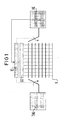
- the device for producing a test-compatible, largely fault-tolerant configuration for redundantly implemented systolic VLSI systems includes a VLSI system V consisting of the total number N 'arranged in rows and columns, a clock sequence control TC, a test bit generator TBG, and an evaluation unit AE and a selector bit generator SG.
- the clock sequence control TC which controls the sequence of the entire test process, outputs a set of selector bits via the selector bit generator SG, and finally switches the modules for the test process on or off line by line, is on the one hand with the selector bit generator SG, and on the other hand with lines that are not shown Control inputs on the VLSI system, which are indicated in FIG.
- the test bit generator TBG for supplying the input variables is connected line by line to the inputs of the VLSI system V, while the evaluation unit is connected line by line to the outputs of the VLSI system to check the result of the arithmetic operations carried out from the input variables.
- the process for producing a test-compatible, largely fault-tolerant configuration for redundantly implemented systolic VLSI systems initially provides for line-by-line testing of the individual modules. With the help of the selector bit generator SG and "Enable" signals at the control inputs of the VLSI system V, the individual modules are switched in a row in accordance with the 0/1 assignment of selector bits. In the given case, 8 out of 10 modules remain in operation line by line. After activating the individual modules, the A and B input variables are first created for the first line at the inputs of the VLSI system.
- the results of the arithmetic operation carried out are tapped line by line at the outputs of the VLSI system and fed to an evaluation unit AE.
- a new 0/1 assignment of selector bits is generated for the line from the selector bit generator SG and a new selection of in this case 8 out of 10 modules is selected for performing the arithmetic operations.
- This test process is repeated until either all 45 possibilities of an 8 out of 10 configuration of the modules have been tested in one line, or until a configuration has been found which gives a positive result in the computing operations carried out. If this is the case, the selector bits used for this are stored in the control logic, which is explained in FIG. 5.
- the modules in the second, third and all further lines of the VLSI system are then tested by performing the above-mentioned method steps.
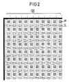
- FIG. 2 shows the arrangement of the modules M in columns and rows within a VLSI system according to the invention.
- the interconnection of the individual modules M with one another is not shown here for the sake of simplicity. It can be seen that each module M is assigned a control logic SL which serves to activate the switches of the corresponding module M.
- the control logic circuits of the modules of a column are each operated by a common selector bit input, while the activation of the modules line by line by supplying an "enable” signal (not shown here), which is supplied to each control logic together in one line.
- This "enable" signal and the 0/1 assignment of the selector bits at the selector bit inputs SBE make it possible to test the modules line by line.
- the regularity of the systolic field requires the control logic to be interconnected, so that one control logic of a module is connected to four other control logic that are in the immediate vicinity of the same. This does not apply to the control logic that is on the periphery of the VLSI system.
- the neighboring control logics are replaced by interconnecting the peripheral control logics with fixed 0 or 1 logic levels. This is indicated in FIG. 2 by the connection of the peripheral control logic with the outer bar boundary, and is explained in more detail in FIG. 5.
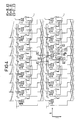
- FIG. 3 shows the input variables which are fed to the VLSI system during normal operation with a matrix-matrix multiplication.
- the input variables for the remaining modules in the remaining lines are analogous. For the configuration procedure, it is most sensible to select the input variables for each module in order to test the modules in order to be able to carry out a quick and simple check for a positive or negative result after the arithmetic operations have been carried out.
- FIG. 4 shows the interconnection of the modules, the illustration of which was omitted in FIG. 2 due to the clarity.
- the interconnection of the module M jk is given here as a representative of the interconnection of the other modules in the rows and columns of the VLSI system.
- the module M jk is connected at one input via a register R1 to 5 B switches BS, at another input via a register R2 to three A switches and at the output above the switch S to two output registers R3 and R4 connected in series.
- the A switches AS, B switches BS and C switches CS are located in front of the registers.
- the A and C switches establish connections between the modules in the row, while the B switches BS are responsible for connecting the modules in columns.
- a connection which is connected on the one hand between the register R1 and the input of the module M jk belonging to the register R1, on the other hand connects five further B switches of the module in the next lower j + 1 th line. These B switches are arranged in the j + 1-th row in the k-2-th, k-1-th, k, k + 1-th and k + 2-th column. Likewise, the connects B-switch BS of the module M jk five further modules are located in the next higher j-1 th row, each of which is in the k-2 th, k-1 th, k, k + 1 th and k + 2 -th column.
- a further connecting line which is connected between register R2 and the input of module M jk belonging to register R2, on the other hand connects the A switches of the modules on the right and the next but one on the right, which are in the k + 1-th and k + 2 -th column of the same row.
- the A-switches AS which are connected upstream of the register R2, enable a connection either to the input of the module on the left in the same line, to which a further register is assigned analogously to the register R1, in the k-1 th column, and a connection with the A switches of the modules in the k-2-th and k-3-th column of the same row.
- a connection to the A switches of the modules in the k + 1-th and k + 2-th column of the same line is made possible.
- the output of the module M jk is switched via a switch S to two output registers R3 and R4 which are connected in series, the output of the output register R4 being a connection to further C switches of the modules on the right and the next but one in the k + 1-th and Allows k + 2nd column of the same row.
- the switch S optionally switches the output of the module M jk or one of the three C switches CS of the module M jk to the output register R3.
- the C switch CS continues to connect the output register R3 via the switch S optionally to the two output registers of the modules connected in series, which are in the same row, but k-3rd, k-2nd and k-1st column are arranged.
- the A switch AS and the C switch CS of the module M jk are switched synchronously, ie the A switch AS provides a connection between the register R2 of the module M jk to the input belonging to the register R2 in the k-1- ten column and the same row arranged module, so the C switch via the switch S connects with the output register R3 of the module M jk to the two series-connected output registers of the module arranged in the k-1 th column and the same row. This applies to the remaining two switches of the A switch AS and C switch CS.
- FIG. 5 shows the control logic, which is split into a fault-tolerant part SLFI and a fault-tolerant part SLF.
- the A, B and C switches AS, BS, CS of the relevant module M jk are controlled.
- a total of ten logic variables must be made available to the control logic.
- the horizontal control line string is four bits wide and includes the logical variables Z j, k-1 , C j, k-1 , D j, k-1 and E j, k-1 or Z j, k , C j, k , D j, k and E j, k ;
- the vertical control line string is six bits wide and results from the logical variables C j, k , E j-1, k-1 , D j-1, k-1 , C j-1, k-1 , C j-1, k and C j-1, k + 1 and C j + 1, k , E j, k-1 , D j, k-1 , C j, k-1 , C j, k and C j, k + 1 .
- the local control logic is implemented redundantly. This is only possible with skillful assignment of the A, B and C switches AS, BS, CS, in that the control logic acts on the module M jk via the switches. Then an error in the control logic only affects the module M jk .
- the part of the control logic SLFI that passes the horizontal information on to the rest of the line is not fault-tolerant, because an error would be adopted by all the remaining modules.
- the control logic SLF that processes the vertical information is fault-tolerant, because incorrect information is only carried up to the module of the next line and can be reconfigured there.
- the fault-tolerant part of the control logic SLF is five times larger than the fault-tolerant part SLFI.
- the horizontal control line string which passes the information on to the rest of the line, is four bits wide and contains three control lines which contain the logic output variables Z j, k , D j, k and E j, k deliver, and are generated from the fault-intolerant part SLFI of the control logic.
- a fourth logical variable C j, k is obtained from the vertical control line via a latch L in the fault-tolerant control logic part.
- the vertical control wiring harness which passes the information on to modules in the next line, is six bits wide and consists of the logical variables D j, k-1 , E j, k-1 , C j, k-1 , C j, k , C j + 1, k and C j, k + 1 .
- the first four logical variables are generated directly from the corresponding logical input variables, while the last two logical variables are taken from neighboring control logics.
- the logical variable C j, k is applied to all control logic of the kth line, at the same time it forms part of the selector bit inputs SBE from FIG. 2. Furthermore, to activate the control logic located in a specific line, the fault-tolerant part SLF is additionally activated -Signal EN or EN 'supplied respectively for the j-th and j + 1-th line. Since one "Enable" signal is assigned to each line for the control logic, there is a total of eight “Enable” signals for the entire VLSI system. With the help of the logical input variables C j, k and the "Enable” signals, it is possible to activate or deactivate each individual module in the VLSI system during the configuration algorithm.
- FIG. 5 A circuit at gate level for the control logic according to FIG. 5 is shown in FIG.
- the ten logical input variables for the control logic are C j, k , E j, k-1 , D j, k-1 , C j, k-1 , Z j, k-1 , C j-1, k + 1 , C j-1, k , E j-1 , k-1 , D j -1 , k-1 and C j-1, k-1 .
- the logic output variables of the control logic are as follows: C j, k , E j, k , D j, k , Z j, k , D j, k , E j, k .
- the interconnection of the eight NAND gates, fifteen inverters and a NOR gate is as follows:
- the logical input variable C j, k forms a logical output variable C j, k on the one hand, and on the other hand it has a first input of a first NAND -Gatters N1 switched, a second logical input variable E j, k-1 is connected to a second input of the first NAND gate N1 and to a first input of a first NOR gate NO1.
- the logic input variable C j, k is connected to the second input of the first NOR gate NO1, and the logic input variable D j, k-1 is connected to the first input of a second NAND gate N2.
- An output of the first NAND gate N1 is connected to a first input of a third NAND gate N3 and the logic input variable C j, k is connected via a first inverter I1 to a first input of a fourth NAND gate N4.
- An output of the first NAND gate N1 supplies the logic output variable via a second inverter I2 E j, k .
- An output of the first NOR gate NO1 is connected via a third inverter I3 to the second input of the second NAND gate N2 and an output of the second NAND gate N2 via a fourth inverter I4 is on the one hand connected to a second input of the third NAND gate N2.
- Gate N3 connected and on the other hand supplies the logical output variable D j, k .
- the logical input variable C j, k-1 is connected via a fifth inverter I5 to a second input of the fourth NAND gate N4 and an output of the fourth NAND gate N4 via a sixth inverter I6 provides the logical output variable Z j, k .
- the output of the second NAND gate N2 provides the logic output variable D j, k and an output of the third NAND gate N3 supplies the logic output variable E j, k via a seventh inverter I7. D j, k .
- the logical input variable C j, k-1 results on the one hand in the logical output variable C j, k-1 and on the other hand provides an eighth Inverter I8 the logical output variable C j, k-1 .
- the logical input variable Z j, k-1 on the one hand forms the logical output variable Z j, k-1 and also supplies the logical output variable via a ninth inverter I9 Z j, k-1 .
- the logical input variable C j-1, k + 1 results in the output variable C j-1, k + 1 and supplies the negated output variable via a tenth inverter I10 C j-1, k + 1 .
- the logical input variable C j-1, k also results in the logical output variable C j-1, k and is connected to a first input of a fifth NAND gate N5 and to a first input of a second NOR gate NO2.
- the logical input variable E j-1, k-1 is connected on the one hand to the second input of the fifth NAND gate N5 and on the other hand to a second input of the second NOR gate NO2, the output of the fifth NAND gate N5 supplies the logic output variable via an eleventh inverter I11 E j-1, k .
- the output of the second NOR gate NO2 is connected to a sixth NAND gate N6 via a twelfth inverter I12, wherein the logic output variable D j-1, k can be tapped at the output of the sixth NAND gate N6 and can be tapped via a 13th Inverter I13 the logical output variable D j-1, k delivers.
- the output of the fifth NAND gate N5 and the output of the 13th inverter I13 are each connected to an input of a seventh NAND gate N7 and the output of the seventh NAND gate N7 is connected to a 14th inverter I14, the output of which logical output variable E j-1, k . D j-1, k can be tapped.
- the logical input variable D j-1, k-1 is connected on the one hand to a second input of the sixth NAND gate N6 and, on the other hand, to a first input of an eighth NAND gate N8 and the logic input variable E j-1, k-1 corresponds to the logical output variable E j-1, k-1 and can be tapped via a 16th inverter I16 as a logic output variable E j-1, k-1 .
- the output of the 16th inverter I16 is connected to a second input of the eighth NAND gate N8 and the output of the eighth NAND gate N8 is coupled to a 15th inverter I15, at whose output the logic output variable E j-1, k- 1st D j-1, k-1 tapped can be.
- the logical input variable C j-1, k-1 also forms the logical output variable C j-1, k-1 .
- Figures 7a to d give the error configurations that activate the switch B1, as well as their gate implementation of the associated logical equation. at.
- the switch B1 establishes a connection between the module M j-1, k and the module M j, k , ie a connection between two modules that are located in the k-th column and in each case in the j-th and j-1- line.
- the prerequisite for this is that both modules are functional.
- the connecting lines between the modules according to FIGS. 7a to 7c indicate that these modules take part in the arithmetic operations, for example matrix-matrix multiplication, and are functional, while those modules which are represented by black-filled squares in FIGS.
- the switch B1 establishes the connection between a module M j, k and a module M j-1, k in the k-th column, for example, that means both modules in the k-th column that lying horizontally to each other take part in the arithmetic operations, for example the matrix-matrix multiplication.
- B1 C j-1, k . C j, k . ( E j-1, k . E j, k ) + (E j-1, k . E j, k . D j-1, k . D j, k ) + (D j-1, k . D j, k )).
- the B1 switch is constructed by a total of six NAND gates N9, N10, N11, N12, N13 and N1 'and by two inverters I17 and I18.
- the logical output variables from the control logic in accordance with FIG. 6 are each connected to the inputs of the NAND gates N9, N10, N11, N12 and N13.
- the logical output variable E j, k as well as the logical output variable E j-1, k is applied to an input of the ninth NAND gate N9, the logic output variables E j, k . D j, k as well as the logical output variables E j-1, k .
- D j-1, k are each connected to an input of the NAND gate N10 and finally the logic output variables D j, k and D j-1, k are applied to inputs of the NAND gate N11.
- the outputs of the ninth NAND gate N9, the tenth NAND gate N10 and the eleventh NAND gate N11 are each switched to an input of a three-input NAND gate N1 ', the output of which is present at an input of the NAND gate N12 .
- the second input of the NAND gate N12 is connected to the logic output variable C j-1, k , while the output of the twelfth NAND gate N12 is connected to an input of the 13th NAND gate N13 via a 17th inverter I17.
- the second input of the thirteenth NAND gate N13 is connected to the logic output variable C j, k and the output signal for the B1 switch can be tapped off at the output of the 13th NAND gate N13 via an 18th inverter I18.
- FIGS. 8a to 8c indicate the error configurations which activate the switch B2 and the implementation at the gate level for its control. Faulty or defective modules are again identified by black squares in FIGS. 8a and 8b.
- the B2 switch establishes a connection from modules M j-1, k + 1 with modules M j, k . This means a connection, for example between a module of the j-1 th row and k + 1 th column to a module in the j th row of j-th row and k-th column k-th column.
- the prerequisite is that both modules are functional. It can be seen from FIG. 8a that exactly one defective module occurs in the j-1 th line up to the k th column, while in FIG.
- B2 C j, k . C j-1, k-1 . ((E j-1, k . D j-1, k ) + (E j, k . D j-1, k . D j, k )).
- FIG. 8 c An implementation according to this logical definition of the B2 switch is shown in Figure 8 c. It consists of a total of five NAND gates N14, N15, N16, N17 and N18 and two inverters I19 and I20.
- the logic output variables from the control logic according to FIG. 6 are switched again to inputs of these NAND gates.
- the logical output variables E j, k . D j, k as well as the logic output variable D j-1, k if each on inputs of the 14th NAND gate N14 and the logic output variables from the control logic E j, k and the logic output variable E j-1, k . D j-1, k each connected to inputs of the 15th NAND gate N15.
- the outputs of the 14th NAND gate N14 and the 15th NAND gate N15 are each switched to inputs of the 16th NAND gate N16. Its output is in turn connected to an input of the 17th NAND gate N17.
- the second input of the 17th NAND gate N17 is connected to the logic output variable C j-1, k + 1 and the output of the 17th NAND gate N17 via a 19th inverter I19 with an input of the 18th NAND gate N18 connected.
- the second input of this 18th NAND gate is again with a Logical output variables C j, k connected and the output of the 18th NAND gate forms the output of the B2 switch via the 20th inverter I20.
- FIGS. 9a and 9b Error configurations which activate the switch B3 are shown in FIGS. 9a and 9b and a realization of their activation at gate level is shown in FIG. 9c.
- the switch B3 establishes a connection between a module M j-1, k + 2 to a module M j, k .
- the prerequisite for this is again that these modules are functional.
- FIGS. 9a and 9b shows that exactly two malfunctioning or defective modules occur in each of the two figures in the j-1 th line.
- Switch B3 is activated precisely when the number of defective modules in the j-1 th row to the k + 1 th row column is just 2. Faulty modules are again identified by black squares in FIGS. 9a and 9b.
- B3 C j, k . E j, k . (D j-1, k + C j-1, k + 1 . E j-1, k . D j-1, k )).
- FIG. 9c The implementation of this logical definition by four NAND gates N19, N20, N21 and N22 and by two inverters I21 and I22 is shown in FIG. 9c.
- Logical output variables from the control logic according to FIG. 6 are in turn connected to the four NAND gates.
- D j-1, k are each switched to inputs of the 19th NAND gate N19, the output of which is connected to an input of the 20th NAND gate N20.
- a second input of the 20th NAND gate N20 is assigned the logic output variable D j-1, k busy.
- the output of the 20th NAND gate N20 is connected to an input of the 21st NAND gate N21, the second input of which is the logic input variable E j, k lies on.
- the output of the 21st NAND gate N21 is via an In verter I21 connected to an input of the 22nd NAND gate N22.
- the logic output variable C j, k is switched to the second input of the 22nd NAND gate N22 and the output of the 22nd NAND gate N22 forms the output of the B3 switch via the inverter I22.
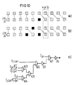
- FIGS. 10a and 10b indicate the error configuration which activate the switch B4 and FIG. 10c shows an implementation of its activation at the gate level.
- the switch B4 establishes a connection between a module M j-1, k-1 and a module M j, k . This means a connection between a module from the j-1 th row and k-1 th column to a module in the j th row j-th ze and k-th column k-th column. that both modules are functional.
- a comparison between FIGS. 10a and 10b shows that in each case there is one more inoperable module in the jth row than in the jth row.
- the switch B4 is then activated when the difference in the number of inoperable modules between the j-th and j-1-th rows up to the k-1-th column, including even 1. Faulty modules are identified by black squares, as in FIGS. 7 to 9.
- B4 C j-1, k-1 . C j, k . (( E j-1, k-1 . E j, k . D j, k ) + (E j-1, k-1 . D j-1, k-1 . D j, k )).
- FIG. 10c The implementation of this logical definition is shown in FIG. 10c. It contains five NAND gates N23, N24, N25, N26 and N27 as well as two inverters I23 and I24.
- the logic output variables of the control logic according to FIG. 6 are in turn connected to the NAND inputs, with the logic output variable D j, k and the output variable E j-1, k-1 .
- D j-1, k-1 each to an input of the 24th NAND gate and the logic output variable E j, k .
- D j, k such as E j-1, k-1 are connected to one input of the 23rd NAND gate.
- the output of the 23rd NAND gate N23 and the 24th NAND gate N24 is in each case connected to an input of the 25th NAND gate N25 and an output of the 25th NAND gate is connected to an input of the 26th NAND gate N26.
- Another input of the NAND gate N26 is assigned the logic output variable C j-1, k-1 and the output of the 26th NAND gate is connected via a 23rd inverter I23 to an input of the 27th NAND gate N27.
- the logic output variable C j, k is connected to a further input of the NAND gate N27, the output of the NAND gate N27 forms the output of the switch B4 via an inverter I24.
- FIGS. 11a and 11b show error configurations which activate the last of the B switches B5, and FIG. 11c shows an implementation at gate level for actuating the switch B5.
- the switch B5 establishes a connection between a module M j-1, k-2 and a module M j, k , ie between a module in the j-1 th row and k-2 th column and a module in FIG j-th row j-th row and k-th column k-th column.
- the prerequisite for this is that the module M j, k is functional.
- 11a and 11b shows that two faulty modules occur in each case in the jth line, of which, however, two faulty modules follow one behind the other in one line in FIG. 11a and in the jth line in FIG. 11b there is at least one functional module between each defective module.
- a faulty module occurs in the j-1 th row and k-1 th column, and in FIG. 11 b in the j-1 th row and k th column.
- the switch B5 is activated precisely when there are no faulty modules in the j-1st row up to the k-2nd column and in the jth row up to the kth column two inoperative modules.
- B5 C j, k . D j, k . ( E j-1, k-1 + (E j-1, k-1 . D j-1, k-1 . C j-1, k-1 )).
- FIG. 11c A realization of this logical definition at gate level by four NAND gates N28, N29, N30 and N31 and by three inverters I25, I26 and I27 is shown in FIG. 11c.
- the logic output variable C j-1, k-1 is fed via a 25th inverter I25 to an input of the 28th NAND gate N28, at the second input of which the logic output variable E j-1, k-1 .
- D j-1, k-1 connected.
- the output of the NAND gate N28 is connected to an input of the 29th NAND gate N29, to the second input of which the logic output variable E j-1, k-1 is applied.
- the output of the 29th NAND gate is connected to an input of the 30th NAND gate N30, the second input of which is occupied by the logic output variable D j, k .
- the output of the NAND gate N30 is connected via a 26th inverter I26 to the 31st NAND gate N31, to the second input of which the logic output variable C j, k is connected.
- the output of the NAND gate N31 is passed through a 27th inverter I27 and forms the output of the switch B5.
- FIG. 1 The implementation for controlling the three A and three C switches, which each have the same control logic, is shown in FIG.
- a realization of these logical equations is made possible by three NAND gates N32, N2 ', N3' and three inverters I28, I29 and I30.
- the logical output variable C j, k and C j, k-1 are each connected to an input of the 32nd NAND gate N32 and the logical output variable C j, k is also connected to an input of the three-input NAND gate N2 ' and connected to an input of the three-input NAND gate N3 '.
- the logical output variables are also connected to the NAND gate N2 ' C j, k-1 and Z j, k-1 and to the NAND gate N3 'the logic output variables C j, k-1 and Z j, k-1 .
- the Outputs of the three NAND gates are each passed through an inverter, so that the output of the 32nd NAND gate via a 28th inverter I28 forms a first output for driving the A1 or C1 switch and the output of the NAND gate N2 'via a 29th inverter I29 the second output for controlling the A2 or C2 switch.
- the output of the NAND gate N3 ' is also connected via a 30th inverter I30 and forms the third output for controlling the A3 or. C3 switch.
Landscapes
- Engineering & Computer Science (AREA)
- General Engineering & Computer Science (AREA)
- Physics & Mathematics (AREA)
- General Physics & Mathematics (AREA)
- Computer Hardware Design (AREA)
- Theoretical Computer Science (AREA)
- Computing Systems (AREA)
- Hardware Redundancy (AREA)
- Tests Of Electronic Circuits (AREA)
- Semiconductor Integrated Circuits (AREA)
- Design And Manufacture Of Integrated Circuits (AREA)
Applications Claiming Priority (2)
| Application Number | Priority Date | Filing Date | Title |
|---|---|---|---|
| DE3731833 | 1987-09-22 | ||
| DE3731833 | 1987-09-22 |
Publications (3)
| Publication Number | Publication Date |
|---|---|
| EP0308660A2 true EP0308660A2 (fr) | 1989-03-29 |
| EP0308660A3 EP0308660A3 (en) | 1990-09-26 |
| EP0308660B1 EP0308660B1 (fr) | 1995-05-24 |
Family
ID=6336564
Family Applications (1)
| Application Number | Title | Priority Date | Filing Date |
|---|---|---|---|
| EP88113627A Expired - Lifetime EP0308660B1 (fr) | 1987-09-22 | 1988-08-22 | Dispositif de fabrication de systèmes systoliques VLSI configuration de redondance, compatible au test et tolérant largement les fautes |
Country Status (4)
| Country | Link |
|---|---|
| US (1) | US4951220A (fr) |
| EP (1) | EP0308660B1 (fr) |
| JP (1) | JPH01101652A (fr) |
| DE (1) | DE3853860D1 (fr) |
Cited By (1)
| Publication number | Priority date | Publication date | Assignee | Title |
|---|---|---|---|---|
| GB2231985A (en) * | 1989-03-31 | 1990-11-28 | American Telephone & Telegraph | Reconfigurable signal processor |
Families Citing this family (38)
| Publication number | Priority date | Publication date | Assignee | Title |
|---|---|---|---|---|
| US5452231A (en) * | 1988-10-05 | 1995-09-19 | Quickturn Design Systems, Inc. | Hierarchically connected reconfigurable logic assembly |
| US5329470A (en) * | 1988-12-02 | 1994-07-12 | Quickturn Systems, Inc. | Reconfigurable hardware emulation system |
| US5109353A (en) * | 1988-12-02 | 1992-04-28 | Quickturn Systems, Incorporated | Apparatus for emulation of electronic hardware system |
| US5353243A (en) | 1989-05-31 | 1994-10-04 | Synopsys Inc. | Hardware modeling system and method of use |
| US5369593A (en) * | 1989-05-31 | 1994-11-29 | Synopsys Inc. | System for and method of connecting a hardware modeling element to a hardware modeling system |
| US5280607A (en) * | 1991-06-28 | 1994-01-18 | International Business Machines Corporation | Method and apparatus for tolerating faults in mesh architectures |
| US5179378A (en) * | 1991-07-30 | 1993-01-12 | University Of South Florida | Method and apparatus for the compression and decompression of data using Lempel-Ziv based techniques |
| US5271014A (en) * | 1992-05-04 | 1993-12-14 | International Business Machines Corporation | Method and apparatus for a fault-tolerant mesh with spare nodes |
| US5513313A (en) * | 1993-01-19 | 1996-04-30 | International Business Machines Corporation | Method for generating hierarchical fault-tolerant mesh architectures |
| US5680583A (en) | 1994-02-16 | 1997-10-21 | Arkos Design, Inc. | Method and apparatus for a trace buffer in an emulation system |
| US5841967A (en) * | 1996-10-17 | 1998-11-24 | Quickturn Design Systems, Inc. | Method and apparatus for design verification using emulation and simulation |
| US6321366B1 (en) | 1997-05-02 | 2001-11-20 | Axis Systems, Inc. | Timing-insensitive glitch-free logic system and method |
| US6134516A (en) * | 1997-05-02 | 2000-10-17 | Axis Systems, Inc. | Simulation server system and method |
| US6009256A (en) * | 1997-05-02 | 1999-12-28 | Axis Systems, Inc. | Simulation/emulation system and method |
| US6026230A (en) * | 1997-05-02 | 2000-02-15 | Axis Systems, Inc. | Memory simulation system and method |
| US6421251B1 (en) | 1997-05-02 | 2002-07-16 | Axis Systems Inc | Array board interconnect system and method |
| US6389379B1 (en) | 1997-05-02 | 2002-05-14 | Axis Systems, Inc. | Converification system and method |
| US5960191A (en) | 1997-05-30 | 1999-09-28 | Quickturn Design Systems, Inc. | Emulation system with time-multiplexed interconnect |
| US5970240A (en) | 1997-06-25 | 1999-10-19 | Quickturn Design Systems, Inc. | Method and apparatus for configurable memory emulation |
| US6092123A (en) * | 1997-07-17 | 2000-07-18 | International Business Machines Corporation | Method and apparatus for changing functions of a hardware device using two or more communication channels |
| US8775997B2 (en) | 2003-09-15 | 2014-07-08 | Nvidia Corporation | System and method for testing and configuring semiconductor functional circuits |
| US8788996B2 (en) | 2003-09-15 | 2014-07-22 | Nvidia Corporation | System and method for configuring semiconductor functional circuits |
| US8732644B1 (en) | 2003-09-15 | 2014-05-20 | Nvidia Corporation | Micro electro mechanical switch system and method for testing and configuring semiconductor functional circuits |
| US6880940B1 (en) * | 2003-11-10 | 2005-04-19 | Honda Motor Co., Ltd. | Magnesium mirror base with countermeasures for galvanic corrosion |
| US8711161B1 (en) | 2003-12-18 | 2014-04-29 | Nvidia Corporation | Functional component compensation reconfiguration system and method |
| US8723231B1 (en) | 2004-09-15 | 2014-05-13 | Nvidia Corporation | Semiconductor die micro electro-mechanical switch management system and method |
| US8711156B1 (en) | 2004-09-30 | 2014-04-29 | Nvidia Corporation | Method and system for remapping processing elements in a pipeline of a graphics processing unit |
| US8021193B1 (en) | 2005-04-25 | 2011-09-20 | Nvidia Corporation | Controlled impedance display adapter |
| US7793029B1 (en) | 2005-05-17 | 2010-09-07 | Nvidia Corporation | Translation device apparatus for configuring printed circuit board connectors |
| US9092170B1 (en) | 2005-10-18 | 2015-07-28 | Nvidia Corporation | Method and system for implementing fragment operation processing across a graphics bus interconnect |
| US8417838B2 (en) * | 2005-12-12 | 2013-04-09 | Nvidia Corporation | System and method for configurable digital communication |
| US8412872B1 (en) | 2005-12-12 | 2013-04-02 | Nvidia Corporation | Configurable GPU and method for graphics processing using a configurable GPU |
| US8724483B2 (en) * | 2007-10-22 | 2014-05-13 | Nvidia Corporation | Loopback configuration for bi-directional interfaces |
| US8453019B2 (en) * | 2007-11-06 | 2013-05-28 | Nvidia Corporation | Method and system for a free running strobe tolerant interface |
| US8687639B2 (en) * | 2009-06-04 | 2014-04-01 | Nvidia Corporation | Method and system for ordering posted packets and non-posted packets transfer |
| US9176909B2 (en) | 2009-12-11 | 2015-11-03 | Nvidia Corporation | Aggregating unoccupied PCI-e links to provide greater bandwidth |
| US9331869B2 (en) * | 2010-03-04 | 2016-05-03 | Nvidia Corporation | Input/output request packet handling techniques by a device specific kernel mode driver |
| US9330031B2 (en) | 2011-12-09 | 2016-05-03 | Nvidia Corporation | System and method for calibration of serial links using a serial-to-parallel loopback |
Family Cites Families (15)
| Publication number | Priority date | Publication date | Assignee | Title |
|---|---|---|---|---|
| US3961250A (en) * | 1974-05-08 | 1976-06-01 | International Business Machines Corporation | Logic network test system with simulator oriented fault test generator |
| US4527249A (en) * | 1982-10-22 | 1985-07-02 | Control Data Corporation | Simulator system for logic design validation |
| JPS5985153A (ja) * | 1982-11-08 | 1984-05-17 | Hitachi Ltd | 冗長化制御装置 |
| JPS59119743A (ja) * | 1982-12-25 | 1984-07-11 | Nippon Telegr & Teleph Corp <Ntt> | 集積回路の冗長構成方式 |
| JPS60144851A (ja) * | 1983-12-30 | 1985-07-31 | Fujitsu Ltd | チヤネル制御装置 |
| JPS6142040A (ja) * | 1984-08-03 | 1986-02-28 | Nec Corp | 論理シミユレ−タ |
| JPH073865B2 (ja) * | 1984-08-07 | 1995-01-18 | 富士通株式会社 | 半導体集積回路及び半導体集積回路の試験方法 |
| US4654851A (en) * | 1984-12-24 | 1987-03-31 | Rockwell International Corporation | Multiple data path simulator |
| JPS61217836A (ja) * | 1985-03-22 | 1986-09-27 | Nec Corp | 集積回路 |
| JPS61226844A (ja) * | 1985-03-30 | 1986-10-08 | Nec Corp | 論理回路のシミユレ−シヨン制御方法 |
| CN1012297B (zh) * | 1985-11-13 | 1991-04-03 | 奥尔凯托N·V公司 | 具有内部单元控制和处理的阵列结构 |
| US4763289A (en) * | 1985-12-31 | 1988-08-09 | International Business Machines Corporation | Method for the modeling and fault simulation of complementary metal oxide semiconductor circuits |
| US4769817A (en) * | 1986-01-31 | 1988-09-06 | Zycad Corporation | Concurrent fault simulation for logic designs |
| US4744084A (en) * | 1986-02-27 | 1988-05-10 | Mentor Graphics Corporation | Hardware modeling system and method for simulating portions of electrical circuits |
| US4817094A (en) * | 1986-12-31 | 1989-03-28 | International Business Machines Corporation | Fault tolerant switch with selectable operating modes |
-
1988
- 1988-08-22 DE DE3853860T patent/DE3853860D1/de not_active Expired - Fee Related
- 1988-08-22 EP EP88113627A patent/EP0308660B1/fr not_active Expired - Lifetime
- 1988-08-26 US US07/236,844 patent/US4951220A/en not_active Expired - Fee Related
- 1988-09-16 JP JP63232110A patent/JPH01101652A/ja active Pending
Cited By (2)
| Publication number | Priority date | Publication date | Assignee | Title |
|---|---|---|---|---|
| GB2231985A (en) * | 1989-03-31 | 1990-11-28 | American Telephone & Telegraph | Reconfigurable signal processor |
| GB2231985B (en) * | 1989-03-31 | 1993-12-15 | American Telephone & Telegraph | System for performing concurrent computational processes |
Also Published As
| Publication number | Publication date |
|---|---|
| US4951220A (en) | 1990-08-21 |
| DE3853860D1 (de) | 1995-06-29 |
| JPH01101652A (ja) | 1989-04-19 |
| EP0308660B1 (fr) | 1995-05-24 |
| EP0308660A3 (en) | 1990-09-26 |
Similar Documents
| Publication | Publication Date | Title |
|---|---|---|
| EP0308660B1 (fr) | Dispositif de fabrication de systèmes systoliques VLSI configuration de redondance, compatible au test et tolérant largement les fautes | |
| EP0010173B1 (fr) | Plaquette à semiconducteur avec une possibilité de test améliorée des circuits intégrés monolithiques à grande échelle | |
| DE69030528T2 (de) | Verfahren und Anordnung zum Testen von Schaltungsplatten | |
| DE3750236T2 (de) | Gerät zur In-line-Abfragesteuerung für Datenprozessorprüfung. | |
| DE19531653C2 (de) | Einchip-Mikroprozessor mit eingebauter Selbsttestfunktion | |
| DE69029390T2 (de) | Programmierbare Schaltung für eine neurale Logik | |
| DE68923086T2 (de) | Verfahren zum Testen von hierarchisch organisierten integrierten Schaltungen und integrierte Schaltungen, geeignet für einen solchen Test. | |
| EP0186724B1 (fr) | Dispositif de test et de diagnostic pour une calculatrice numérique | |
| DE69628034T2 (de) | Hochimpedanzmodus für jtag | |
| DE2550342C2 (de) | Schaltungsanordnung zur Prüfung von Matrixanordnungen | |
| DE3049437A1 (de) | Matrixanordnung einer vielzahl von verarbeitungselementen fuer parallelprozessoren | |
| DE3130714A1 (de) | "testsystem fuer integrierte halbleiterschaltungselemente mit integration grossen massstabs" | |
| DE3338333A1 (de) | Logiksimulatorgeraet zur gueltigkeitspruefung einer logikstruktur | |
| DE19510902A1 (de) | Emulation eines Mehrtor-Speichers unter Verwendung von Markierregistern | |
| DE60010614T2 (de) | On-line Prüfung des programmierbaren Verbindungsnetzwerks in einer feldprogrammierbaren Gatteranordnung | |
| DE69432200T2 (de) | Als Zellenmatrix-Netzwerk organisiertes elektronisches System | |
| DE3789782T2 (de) | Mehrstufenvorrichtung mit Redundanz und deren Verwendung in einem Datenverarbeitungsverfahren. | |
| DE3588212T2 (de) | Verfahren und Gerät zum Suchen von Daten | |
| DE2725396C3 (fr) | ||
| EP0766092B1 (fr) | Circuit testable ayant plusieurs blocs de circuit identiques | |
| DE3788617T2 (de) | Vektordatenverarbeitungssystem mit einer E/A-Steuerung für jeden Vektordatenprozessor und einer anderen E/A-Steuerung für mindestens einen anderen Vektordatenprozessor. | |
| DE112014006751B4 (de) | Schlankes serielles Interface für ein Wrapper-Boundary-Register (Vorrichtung und Verfahren) | |
| DE69411259T2 (de) | Automatisches Entwurfsverfahren für digitale elektronische Schaltkreise | |
| DE3689879T2 (de) | Arithmetisch-logische Schaltung. | |
| DE69129728T2 (de) | Operationsanalyseeinrichtung vom Abtastpfadtyp mit nur einem Abtasttaktgeber und nur einer Ausgangsphase für eine integrierte Schaltung |
Legal Events
| Date | Code | Title | Description |
|---|---|---|---|
| PUAI | Public reference made under article 153(3) epc to a published international application that has entered the european phase |
Free format text: ORIGINAL CODE: 0009012 |
|
| AK | Designated contracting states |
Kind code of ref document: A2 Designated state(s): DE FR GB IT |
|
| PUAL | Search report despatched |
Free format text: ORIGINAL CODE: 0009013 |
|
| AK | Designated contracting states |
Kind code of ref document: A3 Designated state(s): DE FR GB IT |
|
| 17P | Request for examination filed |
Effective date: 19910307 |
|
| 17Q | First examination report despatched |
Effective date: 19930805 |
|
| GRAA | (expected) grant |
Free format text: ORIGINAL CODE: 0009210 |
|
| AK | Designated contracting states |
Kind code of ref document: B1 Designated state(s): DE FR GB IT |
|
| REF | Corresponds to: |
Ref document number: 3853860 Country of ref document: DE Date of ref document: 19950629 |
|
| ITF | It: translation for a ep patent filed | ||
| ET | Fr: translation filed | ||
| GBT | Gb: translation of ep patent filed (gb section 77(6)(a)/1977) |
Effective date: 19950807 |
|
| PLBE | No opposition filed within time limit |
Free format text: ORIGINAL CODE: 0009261 |
|
| STAA | Information on the status of an ep patent application or granted ep patent |
Free format text: STATUS: NO OPPOSITION FILED WITHIN TIME LIMIT |
|
| 26N | No opposition filed | ||
| PGFP | Annual fee paid to national office [announced via postgrant information from national office to epo] |
Ref country code: FR Payment date: 19960830 Year of fee payment: 9 |
|
| PGFP | Annual fee paid to national office [announced via postgrant information from national office to epo] |
Ref country code: DE Payment date: 19961022 Year of fee payment: 9 |
|
| PGFP | Annual fee paid to national office [announced via postgrant information from national office to epo] |
Ref country code: GB Payment date: 19970715 Year of fee payment: 10 |
|
| PG25 | Lapsed in a contracting state [announced via postgrant information from national office to epo] |
Ref country code: FR Free format text: LAPSE BECAUSE OF NON-PAYMENT OF DUE FEES Effective date: 19980430 |
|
| PG25 | Lapsed in a contracting state [announced via postgrant information from national office to epo] |
Ref country code: DE Free format text: LAPSE BECAUSE OF NON-PAYMENT OF DUE FEES Effective date: 19980501 |
|
| REG | Reference to a national code |
Ref country code: FR Ref legal event code: ST |
|
| PG25 | Lapsed in a contracting state [announced via postgrant information from national office to epo] |
Ref country code: GB Free format text: LAPSE BECAUSE OF NON-PAYMENT OF DUE FEES Effective date: 19980822 |
|
| GBPC | Gb: european patent ceased through non-payment of renewal fee |
Effective date: 19980822 |
|
| PG25 | Lapsed in a contracting state [announced via postgrant information from national office to epo] |
Ref country code: IT Free format text: LAPSE BECAUSE OF NON-PAYMENT OF DUE FEES;WARNING: LAPSES OF ITALIAN PATENTS WITH EFFECTIVE DATE BEFORE 2007 MAY HAVE OCCURRED AT ANY TIME BEFORE 2007. THE CORRECT EFFECTIVE DATE MAY BE DIFFERENT FROM THE ONE RECORDED. Effective date: 20050822 |