EP0308726A2 - Circuit intégré à l'échelle de la plaquette - Google Patents
Circuit intégré à l'échelle de la plaquette Download PDFInfo
- Publication number
- EP0308726A2 EP0308726A2 EP88114614A EP88114614A EP0308726A2 EP 0308726 A2 EP0308726 A2 EP 0308726A2 EP 88114614 A EP88114614 A EP 88114614A EP 88114614 A EP88114614 A EP 88114614A EP 0308726 A2 EP0308726 A2 EP 0308726A2
- Authority
- EP
- European Patent Office
- Prior art keywords
- integrated circuit
- scale integrated
- wafer scale
- blocks
- wafer
- Prior art date
- Legal status (The legal status is an assumption and is not a legal conclusion. Google has not performed a legal analysis and makes no representation as to the accuracy of the status listed.)
- Withdrawn
Links
Images




Classifications
-
- H—ELECTRICITY
- H10—SEMICONDUCTOR DEVICES; ELECTRIC SOLID-STATE DEVICES NOT OTHERWISE PROVIDED FOR
- H10D—INORGANIC ELECTRIC SEMICONDUCTOR DEVICES
- H10D84/00—Integrated devices formed in or on semiconductor substrates that comprise only semiconducting layers, e.g. on Si wafers or on GaAs-on-Si wafers
- H10D84/90—Masterslice integrated circuits
-
- G—PHYSICS
- G11—INFORMATION STORAGE
- G11C—STATIC STORES
- G11C29/00—Checking stores for correct operation ; Subsequent repair; Testing stores during standby or offline operation
- G11C29/006—Checking stores for correct operation ; Subsequent repair; Testing stores during standby or offline operation at wafer scale level, i.e. wafer scale integration [WSI]
-
- H—ELECTRICITY
- H10—SEMICONDUCTOR DEVICES; ELECTRIC SOLID-STATE DEVICES NOT OTHERWISE PROVIDED FOR
- H10W—GENERIC PACKAGES, INTERCONNECTIONS, CONNECTORS OR OTHER CONSTRUCTIONAL DETAILS OF DEVICES COVERED BY CLASS H10
- H10W20/00—Interconnections in chips, wafers or substrates
- H10W20/01—Manufacture or treatment
- H10W20/031—Manufacture or treatment of conductive parts of the interconnections
-
- H—ELECTRICITY
- H10—SEMICONDUCTOR DEVICES; ELECTRIC SOLID-STATE DEVICES NOT OTHERWISE PROVIDED FOR
- H10W—GENERIC PACKAGES, INTERCONNECTIONS, CONNECTORS OR OTHER CONSTRUCTIONAL DETAILS OF DEVICES COVERED BY CLASS H10
- H10W20/00—Interconnections in chips, wafers or substrates
- H10W20/40—Interconnections external to wafers or substrates, e.g. back-end-of-line [BEOL] metallisations or vias connecting to gate electrodes
- H10W20/41—Interconnections external to wafers or substrates, e.g. back-end-of-line [BEOL] metallisations or vias connecting to gate electrodes characterised by their conductive parts
- H10W20/43—Layouts of interconnections
Definitions
- the present invention relates to an integrated circuit, and more particularly to a so-called wafer scale integrated circuit.
- a monolithic wafer scale integrated circuit generally stands for an integrated circuit in which a plurality of functional blocks formed on a semiconductor wafers are not individually taken out by dicing or a like method but are permitted to operate in the form of a wafer. Further, integrated circuit chips stand for the individual functional blocks that are formed on a wafer and are individually taken out by dicing or a like method. Moreover, a hybrid wafer scale integrated circuit stands for an integrated circuit in which a substrate consists of a semiconductor water on which are formed wirings only or wirings and elements, and in which a semiconductor integrated circuit chip is mounted on the wafer and is electrically connected thereto.
- the wafer scale integrated circuit stands for both the monolithic wafer scale integrated circuit and a hybrid wafer scale integrated circuit.
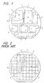
- a plurality of functional blocks 2 of almost equal integration level are formed on a wafer 1, the integration scale of each of the blocks being selected to be nearly that of an LSI chip that is fabricated by an ordinary semiconductor fabrication technology, and malfunctioning blocks that contain defect 3 are not used but good blocks only are used, the input-output signal terminals 4 thereof are globally wired, as required, through a wiring 5, so that the wafer scale integrated circuit as a whole exhibits its functions.
- the wafer scale integrated circuit which as a whole is formed in a single semiconductor wafer is called monolithic wafer scale integrated circuit as mentioned above.
- a semiconductor wafer 6 works chiefly as a wiring substrate, the individual blocks 2′ are formed as separate blocks, and good chips only are connected to the wiring substrate wafer.
- This device is called hybrid wafer scale integrated circuit as mentioned earlier.
- a large computer In designing a computer logic, a large computer must have a logic scale which is greater than that of the conventional LSI's.
- a conventional hybrid wafer scale integrated circuit technology for example, the whole logic is divided into a number of blocks 2′ as shown in Fig. 3. In this case, one block corresponds to one chip.
- r is the same as r of the equation (1)
- B denotes a number of blocks on the wiring substrate
- L denotes the length of a side of a square wiring substrate
- P is the same as P of the equation (1)
- N is an average number of the input-output signal terminals of a block that are contained in a single signal net on the wiring substrate or that are connected to one continuous wiring 5, and which average number in this case may be, for example, about 3.
- the value ⁇ varies depending upon the conditions and may, in one example, be 1 to 3 per a square centimeter. Therefore, it is not easy to economically prepare a chip having a side which is greater than about 1.5 centimeters.
- the yield which is smaller than 10% is far from practicable.
- the functional block includes a semiconductor integrated circuit chip.
- the integration degree of the blocks is so selected that a sufficiently high yield is obtained in compliance with the equation (3) irrespective of whether it is a monolithic wafer scale integrated circuit or a hybrid wafer scale integrated circuit.
- a relatively high packaging density is not achieved as expected.
- a system having a very high terminal density is used as the connection technique, e.g., if a system of solder bumps (which is discussed on page 150 of the aforementioned literature) is used as a connection method for the hybrid wafer scale integrated circuit, it becomes possible to mount any necessary number of chips on the wiring substrate wafer without almost increasing the area of the chip or the area among the chips.
- the conventional monolithic wafer scale integrated circuit as shown in Fig. 2 however, even those blocks that have defects 3 and that do not properly work are contained in the total area of the wafer scale integrated circuit, causing the packaging efficiency to decrease as a whole. With the conventional monolithic wafer scale integrated circuit, therefore, the packaging density becomes smaller than that of the hybrid wafer scale integrated circuit depending upon the conditions.
- the GaAs LSI has an integration scale which is usually smaller than that of the silicon LSI. Because of the aforementioned reasons, therefore, the delay time increases between the LSI's no matter how fast als are propagated in the LSI's. Namely, the high-speed operation is not accomplished even if GaAs is used but rather the operation speed becomes lower than that of when silicon is used.
- the object of the present invention is to provide a wafer scale integrated circuit in which functional blocks of large areas obtained maintaining a high yield are provided on a semiconductor wafer, and the total length of wirings among the functional blocks is shortened, as well as to provide a wafer scale integrated circuit which shortens the signal propagation delay time among the functional blocks, and which has a small redundancy and a high packaging density, overcoming the aforementioned difficulties inherent in the prior art.
- At least one of a plurality of functional blocks constituting the wafer scale integrated circuit has an area that is greater than 2.3 cm2 and the defect in the block is repaired.
- at least one functional block is repaired for its defect among a plurality of functional blocks that constitute the wafer scale integrated circuit, and, furthermore, the above-mentioned block has such a large integration scale (i.e., has an area of greater than 2.3 cm2) that a practical yield can be obtained only by repairing the defect.
- the above practical yield stands for at least about 10%.
- the functional blocks may be repaired using a widely known method of repairing the integrated circuits. An example of the method will be discussed in the embodiment 3 mentioned later.
- the yield according to the present invention can, in practice, be increased to greater than 90%.
- the above functional block whose defect is repaired has i) a cut-away portion in the wiring provided between the insulating layers, and/or ii) an additional wiring portion that connects to a wiring provided between the insulating layers via a hole formed in the insulating layer on the wiring.
- the additional wiring can be composed of, for example, tungsten or molybdenum.
- an element e.g., defective element indicated by numeral 12 in Fig. 4 4) whose wiring is cut, in many cases, is left in the functional block whose defect is repaired.
- the wafer scale integrated circuit according to the present invention can be fabricated according to the following process which comprises:
- the inspection and/or repairing may be effected after the above step iv) has been finished.
- the logic function is inspected for each of the blocks to find the position of defect, the defective portion is cut away, and a spare element and a circuit that have been provided in advance are connected in its place in order to obtain a good block.
- the above method makes it possible to realize a block having an area (at least 2.3 cm2 such as 5 cm2 or 10 cm2) which is much greater than a limit determined by the equation (3).
- the number of input-output signal terminals can be decreased to be much smaller than the number that is given by the equation (1) for which the values a and r are substituted, provided the logic is divided in a size large enough for each block to form a logically desirable unit.
- the system to be constituted by the integrated circuit is a set of macro functions such as arithmetic units and register groups.
- the numbers of input-output terminals of these functional blocks may be smaller than the number of input-output terminals that is derived from Rent's rule expressed by the equation (1) described earlier.
- Rent's rule is an empirical rule that holds true when these functional blocks are logically divided into small groups of functional blocks. Therefore, when the arithmetic units and register groups are used as functional blocks without being divided, they need have input-output terminals in a number smaller than the number of input-output terminals derived according to Rent's rule. For example, an arithmetic unit of fixed decimal point with 100,000 gates has about 1000 input-output terminals.
- each block is a square having a side of 1 cm
- the yield ⁇ is as small as 37% even when ⁇ is one per square centimer in the equation (2).
- the block scale can be selected to be of such a size that is capable of completely accommodating the macro function, i.e., can be selected to have about 50,000 gates, and the input-output signal terminals of each block can be limited to be about 1000.
- the delay time in the case of the macro function mentioned above is 10,000 gates, and a signal path constituted by, for example, the gates of 20 stages crosses the block three times.
- the delay time of the whole signal path is 20 ns
- the delay time in the block is about 14 ns
- the remaining delay time of 6 ns stems from the input-output buffer circuit or wiring among the blocks caused by the crossover of three times between blocks.
- each block when it is attempted to use, for example, GaAs instead of silicon in order to increase the speed, then each block must have a size which is smaller than 10,000 gates. This is because, when GaAs is used, the defect density usually becomes greater than that of when silicon is used.
- the yield (37%) is the same as that of the aforementioned silicon block
- the integration level of the block becomes 2000 gates if the defect density of GaAs is 5/cm2 which is five times as great as that of silicon.
- the signal path crosses the blocks six times.
- the number of crossovers is determined by the number of stages of gates in the block that varies depending upon the integration level of the block.
- the delay time that stems from crossing over the block becomes twice as great, i.e., 12 ns.
- the delay time in the block is reduced to one-half owing to the use of GaAs, i.e., reduced to 7 ns. Therefore, the delay time is 19 ns throughout the entire path, and the effect for high-speed operation is very small compared with the delay time of 20 ns of when silicon is used.
- a block is realized having about 50,000 gates.
- the aforementioned signal path is entirely contained in a single block as described above. Therefore, there no longer exists the delay time of 6 ns that stems from the crossover between blocks, and there exists the delay time of 14 ns only that stems from the block.
- the present invention makes it possible to reduce both the delay time in the block and the delay time that stems from the crossover between blocks. In this case, the delay time could be reduced to about one-third that of the conventional example.
- the number of defects to be repaired increases by 5 times in the above-mentioned example into an average of 25. If a single computer uses 10 blocks, it would be very easy to repair 25 defects per each block.
- Fig. 1 is a plan view for explaining the wafer scale integrated circuit according to the present embodiment, wherein reference numeral 1 denotes a silicon water which is 5 inches in diameter and 0.5 mm in thickness, reference numeral 2 denotes functional blocks in which, for example, symbol A represents an arithmetic unit of a large computer or the like and B denotes an instruction controller. Both of them have sizes of greater than 10 cm2 and more than about 100,000 gates. As will be understood from the aforementioned equation (3), the yield of the individual blocks before being repaired is very small.
- Reference numeral 3 denotes defects. According to this embodiment, the defects 3 are detected for their positions and are all repaired by a method that will be described later.
- Reference numeral 5 denotes a wiring for connecting input-output terminals 4 of the functional blocks 2.
- the functional blocks 2 are formed on the silicon wafers 1 by a known process for manufacturing semiconductors.
- the wirings 5 are also formed by the process for manufacturing semiconductors, and are made up of thin film wirings such as of aluminum.
- the total wiring length of the mutual wirings 5 among the functional blocks can be greatly reduced compared with that of the conventional wafer integrated circuit. Therefore, the total number of wiring layers required for forming the wirings 5 can be decreased to enhance reliability of the mutual wirings.
- the wafer scale integrated circuit according to this embodiment is comprised of seven functional blocks 2 whose macro functions have not been logically divided, and the silicon wafer that serves as a wiring substrate has a side of a length L of about 9 cm. That is, the values B, L in the equations (1) and (2) can be set to be 7 and 9 cm, respectively. Further, the constants a, r can be set to be 2 and 2/3, respectively, as described earlier. In the functional blocks in which the macro functions are not logically divided of this embodiment, furthermore, there does not hold Rent's rule that is expressed by the equation (1). In this embodiment, the number P of the input-output terminals is about 1000. From the equation (2), therefore, the total wiring length W of the wafer scale integrated circuit of the embodiment is about 120 meters.
- the above-mentioned seven functional blocks 2 have sizes of about 10 cm2, though they differ slightly from each other, and have a gate number G of about 100,000.
- the average defect density ⁇ is about 1/cm2.
- the defects are repaired by substituting an element such as a defective transistor by a good element. It is further allowable to replace a defective portion by a good gate or a circuit group of a very small scale.
- the yield of units can be brought to almost 100%. According to the equation (3), for instance, the yield is 37% when the defect density is 1/cm2 and the square block has a side of 1 cm, and the yield is 99.99% when the square block has a side of 100 ⁇ m.
- the units for repair need be formed in a number 10% greater than the required number by taking into consideration the fact that the units for repair are better provided in several kinds and that the defective ones are better replaced by good ones located as close thereto as possible.
- the size of units to be replaced constitutes a circuit group of a size that can be obtained maintaining the yield of about 95%.
- This scale represents a size of about 2 mm if the defect density is 1/cm2 and represents a size of 900 ⁇ m square if the defect density is 5/cm2.
- Figs. 10a to 10c reference numerals 1, 6 denote wafers or substrates, 2 denotes a block, 204 denotes a latch, 203 denotes a gate, and 205 denotes a wiring which connects the latch 204 and the gate 203 together in the block.
- Reference numeral 206 denotes a wiring for connecting the blocks and other blocks.
- a signal sent from a latch A reaches a latch B via 20 gates 203.
- the machine cycle time of the electronic computer is determined by the signal delay time on the signal path. Therefore, a high-speed computer which features short calculation time can be realized as the delay time through the signal path decreases.
- Figs. 10a and 10b illustrate prior art
- Fig. 10c illustrate the art according to the present invention.
- Fig. 10a illustrates the case of prior art using a silicon semiconductor and in which the signal path is constituted chiefly by four blocks 2.
- the blocks have a size of 1 cm x 1 cm and a scale of 10,000 gates.
- the signal path crosses over the blocks three times.
- the signal delay time in the blocks. is 14 ns, and the signal delay time for crossing over among the blocks is 6 ns. Therefore, the signal delay time throughout the whole path is 20 ns.
- Fig. 10b illustrates the case of prior art using a gallium-arsenic (GaAs) semiconductor, and in which the signal path is constituted chiefly by seven blocks 2.
- GaAs gallium-arsenic
- the signal path crosses over the blocks six times as shown in Fig. 10b.
- the signal delay time in the block is halved compared with that of when silicon is used, i.e., is reduced to 7 ns.
- the signal path crosses over the blocks a doubled number of times.
- the signal delay time for crossing over among the blocks becomes 12 ns which is twice as long as that of when silicon is used. Namely, the signal delay time is 19 ns throughout the whole path, and the high-speed operation is not realized compared with when silicon is used.
- Fig. 10c illustrates an example where the present invention is adapted to both of the cases of a macro functional block using silicon and a macro functional block using GaAs.
- the block 2 encompasses the entire signal path. Since there exists no wiring for crossing over the blocks, the signal delay time is 14 ns in the case of silicon and is 7 ns in the case of GaAs, which is one-half that of the former case. Other blocks are not diagramed in Figs. 10a to 10c.
- Fig. 11 The conditions of a signal delay times of these cases are shown in Fig. 11. This embodiment does not involve signal delay time among the blocks, and the signals are transferred at high speeds owing to the reduction in the signal delay time.
- the signal delay time can be reduced to about one-third compared with that of the conventional system which uses silicon.
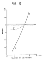
- Fig. 12 is a graph for explaining a relationship between the replacement unit and the redundancy in the case when the defect density is 1/cm2.
- the yield becomes 37% when a side of the replacement unit has a length of as long as 10 mm.
- the redundancy becomes 300% (see point A in Fig. 12).
- the replacement unit is 100 ⁇ m (0.1 mm)
- the yield thereof becomes 99.99% or higher.
- the replacement units may be provided at a rate of one unit per a square centimeter. Therefore, the redundancy is about 0.01% (see point B in Fig.
- a solid line in Fig. 12 represents a curve that is directly derived from the above-mentioned relationship between the redundancy and the yield.
- a broken line in Fig. 12 represents the case where the replacement units are provided in a plurality of types or where the replacement units are formed in a number of more than one per square centimer in order to shorten the distance between the replacement unit and a portion to be repaired as much as possible. Even in this case, the redundancy is suppressed to be smaller than 10% (see point B′ in Fig. 12).
- This embodiment is concerned with repairing the wafer scale integrated circuit discussed in the embodiment 1.
- Figs. 4a and 4b are schematic diagrams for explaining the repairing method according to this embodiment.
- Fig. 4a is a diagram illustrating the state of before being repaired, and wherein reference numeral 12 denotes an element such as a transistor or the like, and reference numerals 10 and 14 denote wirings.
- Reference numeral 13 denotes a defect, i.e., breakage in the wiring 10.
- Reference numeral 15 denotes a short-circuited portion between the wirings 10 and 14, which is a defect, too.
- Reference numeral 16 denotes a spare element. It is presumed here that the element 12 fails to properly operate due to crystal defect in the semiconductor.
- Fig. 4b illustrates the state after Fig.
- reference numeral 20 denotes a rewiring
- 21 denotes connection points
- 18 denotes a cut portion.
- the breakage 13 in the wire is repaired by the rewiring 20.
- the short-circuited portion 15 is repaired by cutting the wiring as designated at 18.
- the element 12 is separated away by the cutting 18 at three portions, and the spare element 16 is connected through connection wirings 19.
- Fig. 5 is a diagram for explaining an example of a method of inspecting and repairing the functional blocks, wherein reference numeral 1 denotes the cross section of the silicon wafer 1 explained in Fig. 1, and 100 denotes a plurality of probes for inspecting the central functional block 2.
- the tip of the probe is brought into contact with the input-output terminals at the periphery of the functional block and with the terminals for measuring.
- a signal for inspection is inputted to the functional block 2 from the probe 100, and an output signal thereof is detected. Owing to the inspection by the probe, position of the defect 3 is roughly indicated.
- the position of defect is pointed out with a circuit which finds AND or OR of input signals as a unit, i.e., with a so-called gate circuit as a unit, such a circuit being constituted by 5 to 6 transistor elements.
- the position of the defect 3 is correctly pointed out by searching the vicinity of the defect 3 of which the position was roughly pointed out in the previous time.
- the electron beam 101 is emitted from a widely known electron beam testing apparatus.
- the tip of the electron beam is smaller than 1 ⁇ m in diameter which is much smaller than the tip of the probe 100.
- the defect 3 is then repaired, i.e., cut, connected and is exchanged by using an ion beam milling machine or a laser CVD (Chemical Vapor Deposition) apparatus.
- Reference numerals 102 and 103 denote tips of ion beam or laser beam emitted from the ion beam milling machine or the laser CVD apparatus.
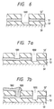
- Fig. 6 is a diagram for explaning an example of the cross section of a wiring that is cut for repairing, wherein reference numeral 51 denotes a wiring such as of aluminum which is formed on a silicon semiconductor wafer or a chip substrate 50 being sandwitched between insulating layers 52 and 52′ which may be composed, for example, of silicon oxide.
- Fig. 6 shows the wiring 51 in a single layer which, however, may be in the form of a multi-layer.
- the layers 51, 52 and 52′ have thicknesses of about 1 to 2 ⁇ m.
- Reference numeral 1000 denotes a hole formed using, for example, the ion beam milling machine, and has a diameter of about 3 ⁇ m. The wiring 51 is cut by the hole 1000 for cutting.
- Figs. 7a and 7b are diagrams for explaining the cross section of the wiring that is repaired according to the embodiment, and wherein the sizes are nearly equal to those of Fig. 6.
- Fig. 7a is a diagram illustrating the state after the hole 1001 for connection and the hole 1000 for cutting are formed.
- the wiring 51 is cut by the hole 1000.
- Fig. 7b is a diagram illustrating the state after the wiring for reconnection or rewiring 1002 is formed.
- the additional wiring 1002 is composed of, for example, tungsten or molybdenum and is formed using an ion beam or a laser CVD. The wiring 51 is thus reconnected or is rewired by the additional wiring 1002 which is electrically connected.
- the functional blocks are finely divided by the partition of logic to enhance the yield to about 30%.
- the functional blocks in which logics are divided must be provided in a plurality of numbers, i.e., must be provided redundantly.
- Fig. 8 is a plan view of a functional block 2′ which is individually cut out from the wafer. Defects have already been repaired by the method explained in conjunction with Figs. 4a to 7b before the functional block 2′ is cut out from the wafer.
- Reference numeral 7 denotes input-output signal terminals and power source terminals which are composed of solder bumps that pertain to widely known connection technology.
- the substrate 6 needs not necessarily be the wafer wiring substrate but may be a conventional multi-layer ceramic substrate.
- the wafer scale integrated circuit of the present invention use is made of functional blocks having large areas obtained by repairing and whereby it is made possible to shorten the total wiring length among the blocks to simplify the complex wiring process required by the wafer scale integrated circuit. Furthermore, the total number of wiring layers is reduced to shorten the signal propagation delay time and to obtain a high packaging density with small redundancy. Therefore, the wafer scale integrated circuit can be very highly densely packaged maintaining high reliability in such applications as data and communication equipment.
- the defects in the functional block are repaired and the yield can be increased up to nearly 100%. Namely, the invention can be adapted to the wafers which may have any large size. Therefore, the yield of functional blocks does not impose any substantial upper limit on the scale of the wafer scale integrated circuit, enabling the scale to be strikingly increased over those of the prior art.
Landscapes
- Design And Manufacture Of Integrated Circuits (AREA)
- Internal Circuitry In Semiconductor Integrated Circuit Devices (AREA)
Applications Claiming Priority (4)
| Application Number | Priority Date | Filing Date | Title |
|---|---|---|---|
| JP237133/87 | 1987-09-24 | ||
| JP23713387 | 1987-09-24 | ||
| JP206309/88 | 1988-08-22 | ||
| JP63206309A JPH01157551A (ja) | 1987-09-24 | 1988-08-22 | ウェーハ・スケール集積回路 |
Publications (2)
| Publication Number | Publication Date |
|---|---|
| EP0308726A2 true EP0308726A2 (fr) | 1989-03-29 |
| EP0308726A3 EP0308726A3 (fr) | 1991-11-21 |
Family
ID=26515575
Family Applications (1)
| Application Number | Title | Priority Date | Filing Date |
|---|---|---|---|
| EP19880114614 Withdrawn EP0308726A3 (fr) | 1987-09-24 | 1988-09-07 | Circuit intégré à l'échelle de la plaquette |
Country Status (3)
| Country | Link |
|---|---|
| EP (1) | EP0308726A3 (fr) |
| JP (1) | JPH01157551A (fr) |
| KR (1) | KR920003798B1 (fr) |
Cited By (1)
| Publication number | Priority date | Publication date | Assignee | Title |
|---|---|---|---|---|
| US9683733B2 (en) | 2010-05-07 | 2017-06-20 | Siemens Aktiengesellschaft | Method for operating a steam generator |
Families Citing this family (1)
| Publication number | Priority date | Publication date | Assignee | Title |
|---|---|---|---|---|
| DE3827802A1 (de) * | 1988-08-16 | 1990-02-22 | Siemens Ag | Chipresidente zwischentreiber fuer diskrete wsi-systeme |
Family Cites Families (1)
| Publication number | Priority date | Publication date | Assignee | Title |
|---|---|---|---|---|
| DE1514902A1 (de) * | 1965-12-07 | 1969-08-14 | Telefunken Patent | Verfahren zum Herstellen integrierter Schaltungen |
-
1988
- 1988-08-22 JP JP63206309A patent/JPH01157551A/ja active Pending
- 1988-09-07 EP EP19880114614 patent/EP0308726A3/fr not_active Withdrawn
- 1988-09-16 KR KR1019880011994A patent/KR920003798B1/ko not_active Expired
Cited By (1)
| Publication number | Priority date | Publication date | Assignee | Title |
|---|---|---|---|---|
| US9683733B2 (en) | 2010-05-07 | 2017-06-20 | Siemens Aktiengesellschaft | Method for operating a steam generator |
Also Published As
| Publication number | Publication date |
|---|---|
| KR920003798B1 (ko) | 1992-05-14 |
| EP0308726A3 (fr) | 1991-11-21 |
| KR890005870A (ko) | 1989-05-17 |
| JPH01157551A (ja) | 1989-06-20 |
Similar Documents
| Publication | Publication Date | Title |
|---|---|---|
| US12021035B2 (en) | Interconnecting dies by stitch routing | |
| US12588494B2 (en) | Die stitching and harvesting of arrayed structures | |
| US5053700A (en) | Method for wafer scale testing of redundant integrated circuit dies | |
| US4956602A (en) | Wafer scale testing of redundant integrated circuit dies | |
| JP3103013B2 (ja) | 集積試験回路付マルチチップ・モジュールおよびその製造方法 | |
| US7061263B1 (en) | Layout and use of bond pads and probe pads for testing of integrated circuits devices | |
| JP3323846B2 (ja) | 高密度探触点を使用した集積回路の製作および試験方法 | |
| US6999332B2 (en) | Semiconductor package with a controlled impedance bus and method of forming same | |
| EP0308726A2 (fr) | Circuit intégré à l'échelle de la plaquette | |
| EP0073721B1 (fr) | Dispositif à semi-conducteur intégré à grand échelle comprenant un détecteur de défauts et son procédé de fabrication | |
| US12564019B2 (en) | Wafer fabrication process and devices with extended peripheral die area | |
| JPH11330256A (ja) | 半導体装置およびその製造方法 | |
| US6768340B2 (en) | Fault-tolerant inverter circuit | |
| CN118299368B (zh) | 一种2.5d封装测试集成电路、测试方法及封装方法 | |
| CN118299284B (zh) | 一种利用晶圆边角区域的封装测试方法 | |
| JPH1082834A (ja) | 半導体集積回路 | |
| JPH0230176A (ja) | 半導体集積回路 | |
| JPH09246387A (ja) | 半導体ウェハおよびそれを用いた半導体集積回路装置、ならびに半導体集積回路装置の製造方法 | |
| CN118538628A (zh) | 一种2.5d封装测试方法及封装方法 | |
| Chaturvedi | Wafer scale integration: a review | |
| JPS58202547A (ja) | 集積回路装置 | |
| JPS62298122A (ja) | 半導体集積回路装置の製造方法 | |
| JPH01291445A (ja) | 半導体装置 | |
| JPH0777561A (ja) | 半導体集積回路装置及び内部回路検査方法 | |
| JPS59134864A (ja) | 半導体集積回路装置構成法およびその実施半導体集積回路装置 |
Legal Events
| Date | Code | Title | Description |
|---|---|---|---|
| PUAI | Public reference made under article 153(3) epc to a published international application that has entered the european phase |
Free format text: ORIGINAL CODE: 0009012 |
|
| AK | Designated contracting states |
Kind code of ref document: A2 Designated state(s): DE FR GB |
|
| 17P | Request for examination filed |
Effective date: 19901114 |
|
| PUAL | Search report despatched |
Free format text: ORIGINAL CODE: 0009013 |
|
| AK | Designated contracting states |
Kind code of ref document: A3 Designated state(s): DE FR GB |
|
| 17Q | First examination report despatched |
Effective date: 19930215 |
|
| STAA | Information on the status of an ep patent application or granted ep patent |
Free format text: STATUS: THE APPLICATION HAS BEEN WITHDRAWN |
|
| 18W | Application withdrawn |
Withdrawal date: 19930615 |